
 Open Access Article
 This Open Access Article is licensed under a
 Creative Commons Attribution 3.0 Unported Licence
Controlled size reduction of rare earth doped nanoparticles for optical quantum technologies
Shuping Liu*a,
Diana Serranoa,
Alexandre Fossatia,
Alexandre Tallairea,
Alban Ferrierab and
Philippe Goldner *a
*a
aChimie ParisTech, PSL University, CNRS, Institut de Recherche de Chimie Paris, F-75005 Paris, France. E-mail: shuping.liu@chimieparistech.psl.eu; philippe.goldner@chimieparistech.psl.eu
bSorbonne Université, Faculté des Sciences et Ingénierie, UFR 933, F-75005 Paris, France
First published on 5th November 2018
Abstract
Rare earth doped nanoparticles with sub-wavelength size can be coupled to optical micro- or nano-cavities to enable efficient single ion readout and control, a key requirement for quantum processors and high-fidelity single-ion quantum memories. However, producing small nanoparticles with good dispersion and exploitable optical coherence properties, another key aspect for these applications, is highly challenging by most synthesis and nano-fabrication methods. We report here on the wet chemical etching of Eu3+:Y2O3 nanoparticles and demonstrate that a controlled size reduction down to 150 nm, well below the wavelength of interest, 580 nm, can be achieved. The etching mechanism is found to proceed by reaction with grain boundaries and isolated grains, based on obtained particles size, morphology and polycrystalline structure. Furthermore, this method allows maintaining long optical coherence lifetimes (T2): the 12.5 μs and 9.3 μs values obtained for 430 nm initial particles and 150 nm etched particles respectively, revealing a broadening of only 10 kHz after etching. These values are the longest T2 values reported for any nanoparticles, opening the way to new rare-earth based nanoscale quantum technologies.
1 Introduction
Trivalent rare earths (REs) doped into a host material are attractive for multiple photonics and optoelectronics applications since they can present sharp absorption and emission lines, high quantum efficiency and no photobleaching.1–4 Recently, since the development of rare-earth doped nanoparticles, they are intensively investigated for bio-imaging,5,6 photodynamic therapy (PDT),6 lighting7 and security.8 In the last years, rare-earth doped crystals have also raised a strong interest in the field of optical quantum technologies, with a focus on quantum information processing and communication.9–12 Because of the shielding of 4f electrons by the outer filled 5s and 5p electron shells, the optical transitions of RE ions can exhibit very narrow optical and spin homogeneous linewidths (Γh) at cryogenic temperatures, or equivalently, long optical and spin coherence lifetimes T2 = (πΓh)−1. T2 corresponds to the lifetime of the superposition, i.e. quantum states that can be created in RE ions and are therefore of utmost importance in quantum technologies applications. Ions of interest in this field include Yb3+,13 Eu3+,14 Er3+,15 Nd3+,16 Pr3+![[thin space (1/6-em)]](https://www.rsc.org/images/entities/char_2009.gif) 17 and Tm3+18 doped into crystals such as Y2SiO5,13–17 YAG18 or YVO4.19 The longest optical coherence lifetime in a solid state system, T2 = 4.4 ms, was obtained in Er3+:Y2SiO5,20 and several hours of spin coherence lifetime have been reported in Eu3+:Y2SiO5.21 These attractive properties, unique in the solid state, allow RE doped crystals to be used as quantum light-matter interfaces, as shown in recent reports on quantum memories and optical to microwave transducers.22–25
17 and Tm3+18 doped into crystals such as Y2SiO5,13–17 YAG18 or YVO4.19 The longest optical coherence lifetime in a solid state system, T2 = 4.4 ms, was obtained in Er3+:Y2SiO5,20 and several hours of spin coherence lifetime have been reported in Eu3+:Y2SiO5.21 These attractive properties, unique in the solid state, allow RE doped crystals to be used as quantum light-matter interfaces, as shown in recent reports on quantum memories and optical to microwave transducers.22–25
Despite the striking demonstrations reported in macroscopic crystals, RE nanoparticles offer key advantages. In particular, nanoscale systems can be placed in a high-quality-factor optical micro- or nano-cavities to take advantage of a stronger light-matter coupling. This can lead to efficient single ion readout,26,27 and in the long term, it could give rise to scalable quantum processors and high fidelity memories for quantum networks.19,28,29
Nonetheless, obtaining long optical and/or spin coherence lifetimes in nano-materials like nano-diamonds30 or RE nano-crystals,31 is an outstanding challenge. This is because quantum states are extremely sensitive to even small time-dependent perturbations like fluctuating magnetic fields produced by impurities or defects carrying electron spins. At the nanoscale, such perturbing centres can form on particles surfaces or be introduced by precursors during the synthesis, which ultimately results in reduced coherence lifetimes. Very high quality materials are therefore needed to reach T2 values comparable to bulk samples. In this sense, Eu3+doped Y2O3 is a particularly interesting candidate: in contrast to other RE materials,27,32–34 Eu3+doped Y2O3 nanoparticles presenting remarkable optical and spin coherence properties, as well as narrow size distribution and bulk-like optical absorption and emission features can be obtained by chemical synthesis.35–37 Our previous studies on Eu3+:Y2O3 nanoparticles synthesized by homogeneous precipitation demonstrated an optical homogeneous linewidth of 45 kHz (T2 = 7 μs) for the Eu3+: 7F0 → 5D0 transition at 580 nm in 400 nm-diameter particles.36 Spin homogeneous linewidth down to 40 Hz (T2 = 8.1 ms) has also been recently reported.37 These results are comparable to values observed in some Eu3+:Y2O3 bulk crystals and transparent ceramics.31,38–41 Still, optical micro-cavities require low scattering losses in order to reach high quality factor and large cavity-ion coupling. Particles significantly smaller than the optical wavelength, 580 nm in the case of Eu3+, are therefore necessary, as the scattering losses scale as the sixth power of the particle size.28
Here, we propose wet chemical etching as a new approach to obtain well-dispersed and sub-wavelength RE doped Y2O3 nanoparticles with narrow homogeneous linewidths. Although the homogeneous precipitation method allows for morphology and size distribution control, the Y2O3 phase forms after calcination of the precipitated yttrium carbonate precursors (Y(OH)CO3·xH2O, YOC). Former investigations demonstrated that high calcination temperature (∼1200 °C) is required to cure defects, achieve sufficient crystalline quality and ensure good optical performance.35,36 However, this also leads to an increase in aggregation and sintering of the particles when their size is decreased. Our approach to prevent this consists in synthesising high-quality and well-dispersed Y2O3 particles with average size in the 400–500 nm range, and then applying chemical etching to achieve a controlled size reduction. This could allow obtaining particles with appropriate size with respect to the optical micro- or nano-cavity targeted quality factor, while preserving the initial particles optical properties. The etching mechanism and the optical coherence performance at 580 nm of Eu3+:Y2O3 etched particles were analyzed and are here discussed. Homogeneous linewidth broadening as low as 10 kHz was measured for 150 nm etched nanoparticles starting from 430 nm initial nanoparticles. The corresponding coherence lifetimes, 9.3 μs and 12.5 μs, are the longest ever reported for any nanoparticles. The results suggest that chemical etching is a promising way to obtain RE doped particles suitable for nanoscale quantum hardware architectures.
2 Materials and methods
The initial 0.3 at% Eu3+:Y2O3 nanoparticles were synthesized by homogeneous precipitation with a calcination temperature of 1200 °C. The detailed technological route has been described in previous work.35 The etching agent used in the study was glacial acetic acid (CH3COOH, original concentration of 100 wt%, with density 1.05 g cm−3). Acetic acid has been previously used as etchant in semiconductor manufacturing processes, with concentrations varying from 20 wt% to 68 wt%.42 The chemical etching experiments were carried out by mixing Eu3+:Y2O3 nanoparticles with fresh acid solutions (50 wt% prepared with deionized water). To ensure homogeneous temperature in the acid solution, etching was done under water-bath, with continuous magnetic agitation. After chemical etching, the nanoparticles were collected by centrifugation and washed several times with deionized water and absolute ethanol to remove the byproducts. The final etched powders were obtained after drying at 80 °C for 24 h. A post microwave treatment under oxygen plasma was performed to remove possible impurities. In order to clarify the effect of various etching conditions on the structures of the nanoparticles, etching time from 1 to 5 h, water-bath temperature from 40 to 70 °C and acetic acid concentration from 40 to 70 wt% were investigated. No dependence on the acetic acid content was found, while the effect of etching time and temperature is later discussed in the manuscript.The morphology of initial and etched particles was observed by scanning electron microscopy (SEM, Zeiss Leo1530) and transmission electron microscopy (TEM, JEOL-JEM-100CXI) operating at 100 kV. The particle size distributions were calculated with Image J software based on at least 300 nanoparticles from different SEM images. X-ray diffraction (XRD) measurements were performed on a Panalytical XPert Pro diffractometer with an incident beam Ge monochromator. Crystallite or single grain sizes were determined from the FWHM of 4 different diffraction peaks by applying the Scherrer equation. Mass losses due to etching were derived from the concentration of yttrium in the etched solutions measured by inductively coupled plasma atomic emission spectrometry (ICP-AES, ThermalFisher icp 6000).43,44
Inhomogeneous and homogeneous linewidths were measured on several initial and etched particles with different average particle size after etching. The samples in form of powders were placed in a helium bath cryostat (Janis SVT-200) and maintained in a copper holder between two glass plates. The detection was carried out by collecting light scattered through the sample as explained in previous works.31,36 Inhomogeneous linewidths (Γinh) were recorded, for the Eu3+: 7F0 → 5D0 transition, at approximately 10 K by fluorescence excitation using a CW dye ring laser (Sirah Matisse DS, 200 kHz linewidth) pumped by a Coherent Verdi G10 laser. A long-pass filter (600 nm cut-off wavelength) was placed in front of the detector (APD Thorlabs 110 A/M) to reject the excitation light. Homogeneous linewidths (Γh) were determined from coherence lifetimes (T2), the latter measured by two pulse photon echo experiments at the center of the 7F0 → 5D0 (580.88 nm in vacuum) transition at 1.4 K. The length of the exciting and rephasing pulses in the sequence was 1 and 1.5 μs respectively.
3 Results and discussion
3.1 Structural characterizations and etching mechanism
Several series of Eu3+doped Y2O3 nanoparticles were synthesized by homogenous precipitation, calcined at 1200 °C, and subsequently etched in acetic acid solutions of 50 wt% acid content (8.53 mol L−1). A weak acid (pKa = 4.76 at 25 °C) was chosen for low etching rates, allowing control over the size reduction process. Fig. 1 shows the evolution of the particle size distribution and morphology as a function of etching time. The initial Eu3+:Y2O3 nanoparticles exhibit spherical, well-dispersed morphology and particle size of 450 ± 56 nm according to log-normal fit. As observed, when etching time increases from 1 to 5 hours, the nanoparticles turn to be gradually smaller and their shape changes, as evidenced by the appearance of sharp edges and facets. It can be noted that the size distribution of the etched particles stays comparable to that of the initial particles, slightly broadening after 4 hours etching (Fig. 1d and e).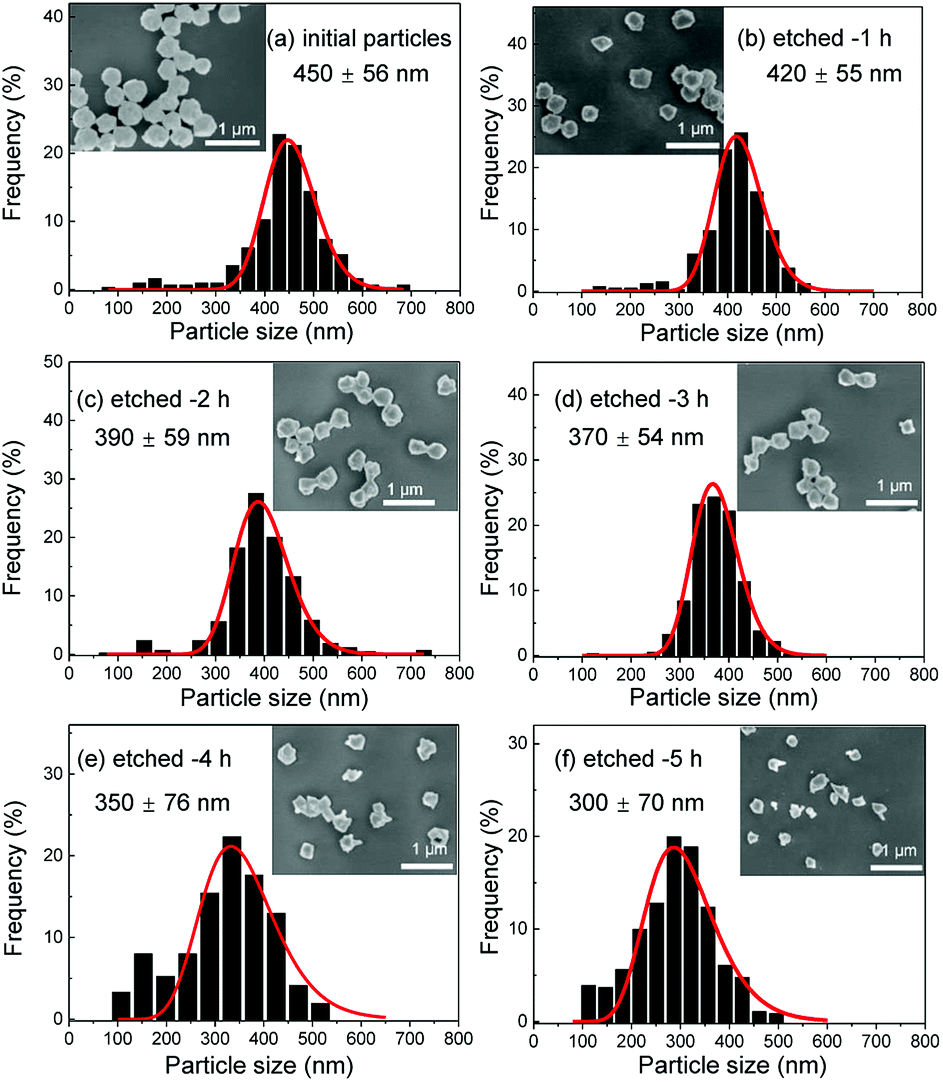 | ||
| Fig. 1 Scanning electron microscopy (SEM) micrographs and size distributions of the initial and etched Eu3+:Y2O3 nanoparticles for etching times increasing from 1 to 5 hours (etching temperature T = 50 °C). | ||
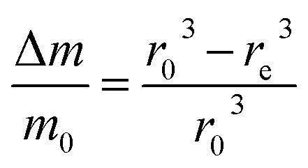
Inductively coupled plasma atomic emission spectroscopy (ICP-AES) was used to determine the mass loss due to etching by measuring the yttrium element concentration in the acid solution after removing the etched particles. In Fig. 2, the ICP-AES results are compared to the expected mass loss based on the progressive size reduction observed in Fig. 1. This simple model assumes that the nanoparticles are perfectly spherical and that the total number of particles remains the same along the etching process. The mass of a single particle is then given by:
 | (1) |
 | (2) |
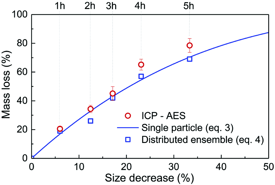 | ||
| Fig. 2 Relative mass loss due to etching as a function of the relative particle size decrease, (r0 − re)/r0, with r0 = 225 nm (initial particles) and re the average radius of the etched particles after different etching times, e.g. r0 = 150 nm for t = 5 h (Fig. 1). The experimental ICP-AES results (red dots) are compared to the mass loss expected from the size reduction model (eqn (3) and (4)) for a single average particle (line) and an ensemble of 1000 particles distributed in size as in Fig. 1 (blue squares). | ||
Then, the relative mass loss per particle just depends on the initial and final particle radii as:
 | (3) |
For an ensemble of particles with total mass  and a distribution of initial and final radii r0,i and re,i, eqn (3) becomes:
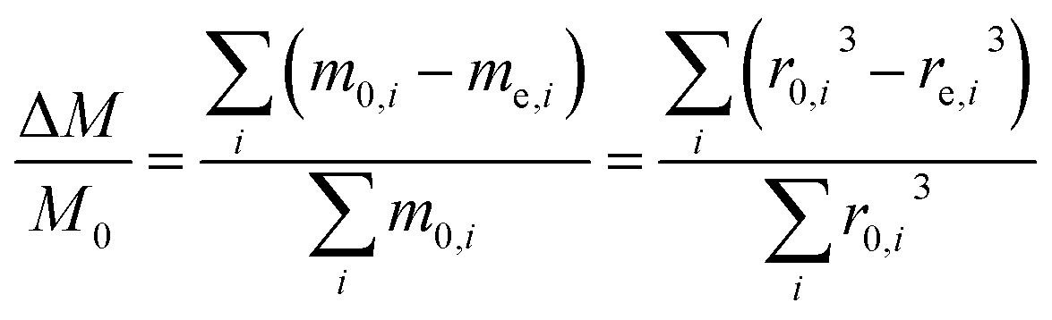 | (4) |
As displayed in Fig. 2, the mass loss trend measured by ICP-AES is rather well described by eqn (3) and (4), some deviation appearing for long etching times (>4 h). A closer insight into the etched particles inner structure nevertheless indicates that this model, just considering an isotropic and continuous volume reduction of the particles, does not provide an accurate description of the etching mechanism taking place here. Indeed, as the initial Eu3+:Y2O3 particles are polycrystalline, they are made of multiple crystalline grains with average sizes ranging from ≈100 to 120 nm. XRD investigations reveal that the etching process does not lead to a noticeable reduction of the grain size nor increases the grain size dispersion (Fig. 3), in disagreement with the continuous volume reduction hypothesis. To explain this observation, we propose that the acid preferentially reacts with grain boundaries, leading to the detachment of small crystal grains as the etching proceeds, as reported in polycrystalline silicon ultra thin films.45 This is supported by TEM images in which nearly detached grains are observed (Fig. 4, red arrows). The mass loss measured by ICP-AES and given in Fig. 2 is mainly attributed to detached grains, which are etched in a rather short time due to their small volume.
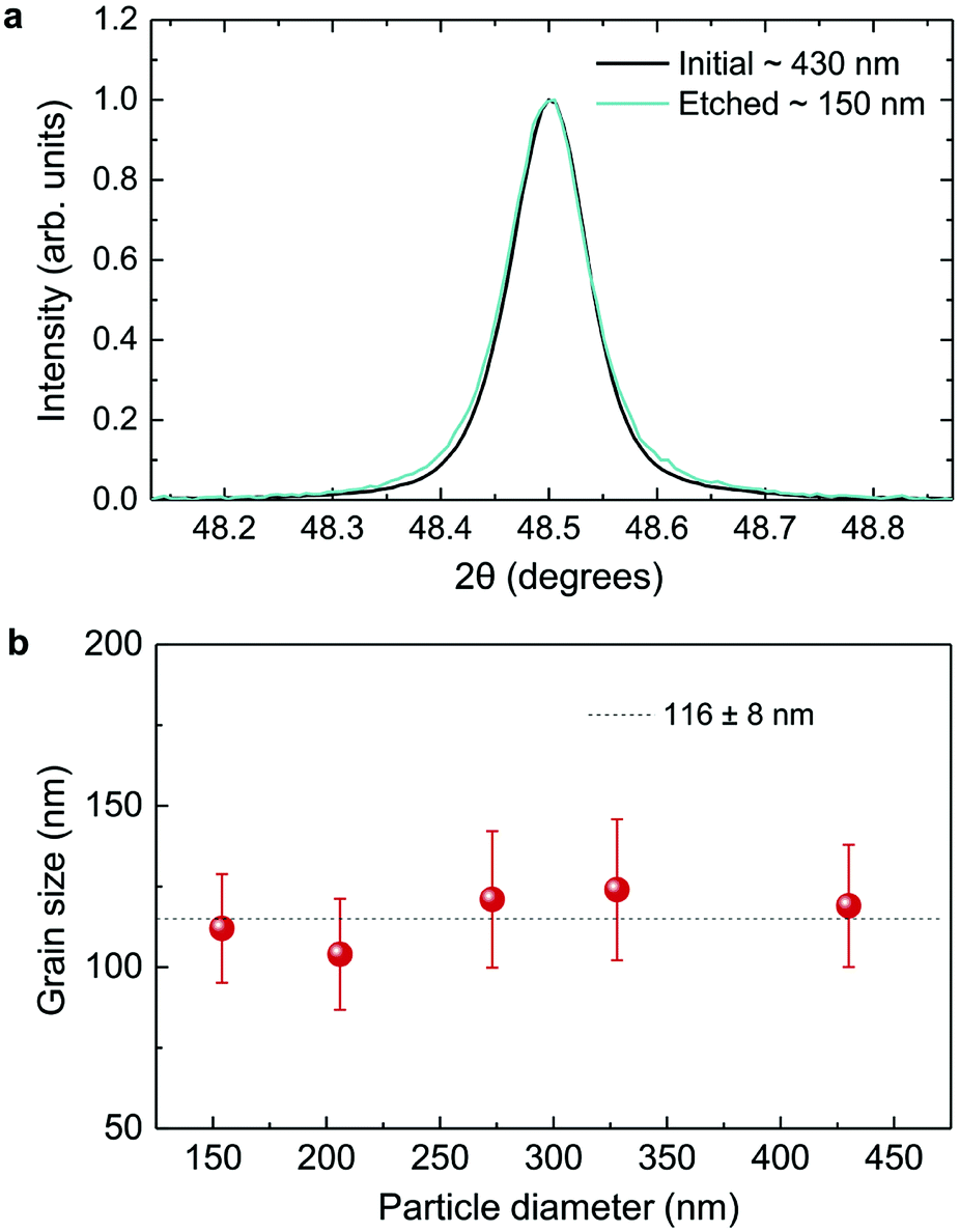 | ||
| Fig. 3 XRD investigation. (a) Normalized diffraction peak for initial and etched particles with average sizes of 430 and 150 nm respectively. (b) Grain size as a function of particle size. The dotted line is a guide to the eye. | ||
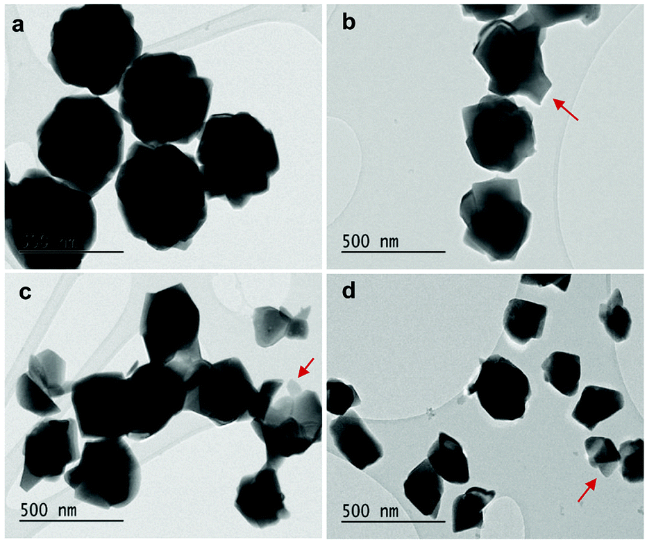 | ||
| Fig. 4 TEM images of (a) initial 450 nm-diameter particles. Etched particles with final average particle size of (b) 400 nm, (c) 340 nm and (d) 200 nm obtained by adjusting etching time and temperature (see Fig. 5). Red arrows: single crystalline grains nearly detached from particles during etching. | ||
Based on the previous conclusions, we redefined the size reduction model by taking into account the polycrystalline nature of the particles, with average grain diameter of 116 ± 8 nm (Fig. 3b). The mass of a single particle then becomes:
 | (5) |
 | (6) |
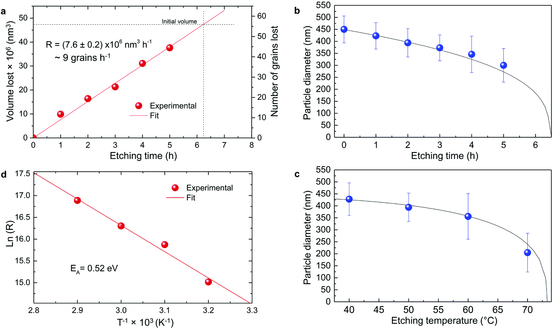 | ||
| Fig. 5 Particle size evolution with etching time and temperature. (a) Volume lost as a function of etching time and corresponding etching rate. (b) Particle size decrease as a function of etching time with T = 50 °C (dots) compared to the particle size evolution expected from a rate of 7.6 × 10⁶ nm3 h−1 (line). (c) Particle size decrease as a function of etching temperature with a fixed etching time of 2 h (dots) compared to the particle size evolution for an activation energy EA = 0.52 eV (line). (d) ln(R) versus T−1 showing a linear dependence from which EA can be estimated according to eqn (8). | ||
The temperature dependence of the etching rate, R(T), was also determined from the particle size decrease as a function of etching temperature for a fixed etching time t. Thus, R(T) was estimated as:
 | (7) |
 | (8) |
In conclusion, it is demonstrated that a controlled size reduction of the initial Eu3+:Y2O3 particles is possible by accurately tuning etching time and temperature. Particles smaller than 150 nm and even single crystalline particles could in principle be obtained by further optimization of both parameters.
3.2 High resolution and coherent spectroscopy
The inhomogeneous broadening (Γinh) of initial and etched particles was recorded at low temperature (∼10 K) by monitoring the Eu3+ 5D0 emissions while scanning a narrow-linewidth single frequency laser through the 7F0 → 5D0 transition (see Methods). The initial particles showed Γinh values around 11 GHz, as expected for particles annealed at 1200 °C.35 After etching, a clear broadening was observed in all measured samples, as in the example shown in Fig. 6. Both the initial and etched particles lineshapes could be described by Lorentzian functions. This denotes point defects as the source of inhomogeneous broadening.47 In non-etched particles, the inhomogeneous broadening is known to be dominated by the Eu3+ ions themselves, highlighting the low content of defects in these materials.35 Substitution of Y3+ by Eu3+ induces strain in the crystalline matrix and therefore broadening because of their different atomic radii: rEu = 0.950 Å, rY = 0.892 Å.48 Upon etching, strain is not expected to change in the crystalline grains since their size is not noticeably changed during the process, as discussed in the previous section. We therefore attribute the additional broadening observed in etched particles to an increase in point defects at the surface of the crystalline grains, in agreement with the Lorentzian lineshape of the transition.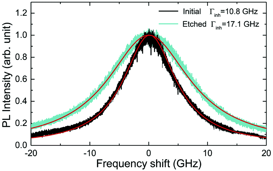 | ||
| Fig. 6 Inhomogeneous broadening (Γinh) of the 7F0 → 5D0 optical transitions in initial (black) and etched (green) nanoparticles with average sizes of 450 and 200 nm respectively. Linewidths were estimated by Lorentzian fit. | ||
In order to determine the impact of etching on the optical coherence of the particles, we measured optical coherence lifetimes (T2) in a series of etched nanoparticles. Starting from an initial size of 430 nm, the smallest particles had an average diameter of 150 nm after etching. Coherence lifetimes and homogeneous linewidths Γh = (πT2)−1 were obtained from two-pulse photon echo measurements31,36 at 1.4 ± 0.1 K (see Methods). As shown in Fig. 7a, they could be fitted by a single exponential, as previously observed in other nanocrystals.31 All measured homogeneous linewidths were below 100 kHz and the additional broadening attributed to etching (Γh,etched − Γh,initial) did not show a clear dependence on particle size as displayed in Fig. 7b. In particular, the smallest particles homogeneous linewidth was broadened by only 10 kHz compared to the initial particles. In a previous study, we attributed the main contributions to Eu3+ homogeneous linewidth in nanoparticles to fluctuations due to residual disorder and surface charges.36 In all likelihood, the additional broadening induced by etching results from surface modifications (Fig. 4). Since the broadening is only weakly dependent on the particle size, it seems probable that it occurs at the crystalline grain level, whose size does not change with etching (Fig. 3). It could be explained by an increase of fluctuations related to disorder, which increases after etching as evidenced by Γinh measurements. Surface charges could also increase after etching due for example to the creation of dangling bonds. Further studies involving temperature dependence of Γh and 3-pulse echoes decays could help clarify this point.36,40
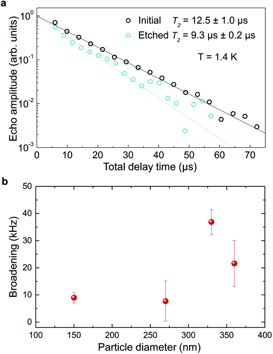 | ||
| Fig. 7 Optical coherence lifetimes and homogeneous broadening. (a) Photon echo decays for initial and etched nanoparticles at 1.4 K with average sizes of 430 and 150 nm respectively. T2 values were derived by single exponential fit to the decay data. (b) Additional broadening due to etching as a function of the particles size. Error bars represent ±1 standard deviation from several measurements. | ||
These results demonstrate that wet chemical etching can be very useful to reduce particle size while maintaining very narrow homogeneous linewidths. For the smallest particles, we are able to decrease particle size by 65%, from 430 nm to 150 nm, (96% reduction in volume), while obtaining Γh = 34.2 kHz, an unmatched value for any nanoparticle to the best of our knowledge. The significance of this linewidth can be illustrated by comparing it with the interactions used to implement quantum gates in rare earth doped crystals.49 Based on Eu3+ optical Stark coefficients, electric dipole–dipole interactions will induce frequency shifts equal to Γh, i.e. 34.2 kHz, for ions separated by about 10 nm.36 In the 150 nm particles, the average distance between Eu3+ ions in the C2 site for 0.3% doped Y2O3 particles is 3.2 nm, whereas a single particle contains about 105 Eu3+ ions. This suggests that a large fraction of ions could interact strongly enough to explore Eu3+–Eu3+ interactions and 2-qubit gates. Furthermore, a fibre micro-cavity containing a 150 nm particle could reach quality factors of a few 1000 s at 580 nm, an increase of nearly three orders of magnitude compared to 400 nm particles, which should be high enough to show enhanced light coupling with Eu3+ ions.28
4 Conclusion
In conclusion, we have found that chemical etching can be used for etching Eu3+:Y2O3 oxide polycrystalline nanoparticles at controlled rates. The particles size can be decreased from initial large particles in the 400–500 nm range to much smaller ones (i.e. 150 nm) with a narrow distribution, good dispersion and without obvious changes on the single crystallite size. Based on imaging and structural analysis we propose an etching mechanism that acetic acid tends to open the grain boundaries in the particles, detaching single crystalline grains that are quickly etched, and effectively reducing the size of the remaining particles. Furthermore, we demonstrate that chemical etching has a limited impact on optical performance of the nanoparticles, leading to homogeneous broadenings below 40 kHz for particles between 360 and 150 nm. Moreover, the coherence times of 12.5 μs (Γh = 25.5 kHz) for 430 nm initial particles and 9.3 μs (Γh = 34.2 kHz) for 150 nm etched nanoparticles observed at 1.4 K, are the longest optical coherence times ever reported for nanoparticles. Our results demonstrate that chemical etching is a promising way to synthesize RE:Y2O3 nanoparticles suitable for coupling with optical micro-cavities and with long coherence lifetimes, opening the way to efficient nanoscale quantum memories and processors.Conflicts of interest
There are no conflicts to declare.Acknowledgements
This project has received funding from the European Union Horizon 2020 research and innovation programme under grant agreement no. 712721 (NanOQTech). We thank Odile Majerus for her assistance in the ICP-AES measurements, Patricia Beaunier for help in the TEM measurements and Thierry Gacoin for useful comments.Notes and references
- M. J. Weber, Handbook on the Physics and Chemistry of Rare Earths, Elsevier, 1979, vol. 4, pp. 275–315 Search PubMed.
- M. J. F. Digonnet, Rare-Earth-Doped Fiber Lasers and Amplifiers, Revised and Expanded, CRC Press, 2001 Search PubMed.
- C. R. Ronda, T. Jüstel and H. Nikol, J. Alloys Compd., 1998, 275–277, 669–676 CrossRef CAS.
- B. C. Rowan, L. R. Wilson and B. S. Richards, IEEE J. Sel. Top. Quantum Electron., 2008, 14, 1312–1322 CAS.
- C. Bouzigues, T. Gacoin and A. Alexandrou, ACS Nano, 2011, 5, 8488–8505 CrossRef CAS PubMed.
- M. Abdesselem, M. Schoeffel, I. Maurin, R. Ramodiharilafy, G. Autret, O. Clḿent, P.-L. Tharaux, J.-P. Boilot, T. Gacoin, C. Bouzigues and A. Alexandrou, ACS Nano, 2014, 8, 11126–11137 CrossRef CAS PubMed.
- G. Sinha and A. Patra, Chem. Phys. Lett., 2009, 473, 151–154 CrossRef CAS.
- W. J. Kim, M. Nyk and P. N. Prasad, Nanotechnology, 2009, 20, 185301 CrossRef PubMed.
- C. W. Thiel, T. Böttger and R. L. Cone, J. Lumin., 2011, 131, 353–361 CrossRef CAS.
- W. Tittel, M. Afzelius, T. Chaneliere, R. L. Cone, S. Kröll, S. A. Moiseev and M. Sellars, Laser Photonics Rev., 2010, 4, 244–267 CrossRef CAS.
- P. Goldner, A. Ferrier and O. Guillot-Noël, Handb. Phys. Chem. Rare Earths, 2015, 46, 1–78 Search PubMed.
- N. Kunkel and P. Goldner, Z. Anorg. Allg. Chem., 2018, 644, 66–76 CrossRef CAS.
- S. Welinski, A. Ferrier, M. Afzelius and P. Goldner, Phys. Rev. B, 2016, 94, 155116 CrossRef.
- R. W. Equall, Y. Sun, R. L. Cone and R. M. Macfarlane, Phys. Rev. Lett., 1994, 72, 2179–2182 CrossRef CAS PubMed.
- T. Böttger, C. W. Thiel, R. L. Cone and Y. Sun, Phys. Rev. B, 2009, 79, 115104 CrossRef.
- I. Usmani, M. Afzelius, H. de Riedmatten and N. Gisin, Nat. Commun., 2010, 1, 12 Search PubMed.
- R. W. Equall, R. L. Cone and R. M. Macfarlane, Phys. Rev. B, 1995, 52, 3963–3969 CrossRef CAS.
- A. Louchet, J. S. Habib, V. Crozatier, I. Lorgeré, F. Goldfarb, F. Bretenaker, J.-L. Le Gouët, O. Guillot-Noël and P. Goldner, Phys. Rev. B, 2007, 75, 035131 CrossRef.
- T. Zhong, J. M. Kindem, J. G. Bartholomew, J. Rochman, I. Craiciu, E. Miyazono, M. Bettinelli, E. Cavalli, V. Verma, S. W. Nam, F. Marsili, M. D. Shaw, A. D. Beyer and A. Faraon, Science, 2017, 357, 1392–1395 CrossRef CAS PubMed.
- T. Böttger, C. W. Thiel, Y. Sun and R. L. Cone, Phys. Rev. B, 2006, 73, 075101 CrossRef.
- M. Zhong, M. P. Hedges, R. L. Ahlefeldt, J. G. Bartholomew, S. E. Beavan, S. M. Wittig, J. J. Longdell and M. J. Sellars, Nature, 2015, 517, 177 CrossRef CAS PubMed.
- F. Bussières, C. Clausen, A. Tiranov, B. Korzh, V. B. Verma, S. W. Nam, F. Marsili, A. Ferrier, P. Goldner, H. Herrmann, C. Silberhorn, W. Sohler, M. Afzelius and N. Gisin, Nat. Photonics, 2014, 8, 775 CrossRef.
- E. Saglamyurek, J. Jin, V. B. Verma, M. D. Shaw, F. Marsili, S. W. Nam, D. Oblak and W. Tittel, Nat. Photonics, 2015, 9, 83 CrossRef CAS.
- N. Maring, P. Farrera, K. Kutluer, M. Mazzera, G. Heinze and H. de Riedmatten, Nature, 2017, 551, 485 CrossRef CAS PubMed.
- L. A. Williamson, Y.-H. Chen and J. J. Longdell, Phys. Rev. Lett., 2014, 113, 203601 CrossRef PubMed.
- R. Kolesov, K. Xia, R. Reuter, R. Stöhr, A. Zappe, J. Meijer, P. R. Hemmer and J. Wrachtrup, Nat. Commun., 2012, 3, 1029 CrossRef CAS PubMed.
- T. Utikal, E. Eichhammer, L. Petersen, A. Renn, S. Götzinger and V. Sandoghdar, Nat. Commun., 2014, 5, 3627 CrossRef CAS PubMed.
- B. Casabone, J. Benedikter, T. Hümmer, F. Beck, K. de Oliveira Lima, T. W. Hänsch, A. Ferrier, P. Goldner, H. de Riedmatten and D. Hunger, New J. Phys., 2018, 20(9), 095006 CrossRef.
- A. Dibos, M. Raha, C. Phenicie and J. Thompson, arXiv:1711.10368v1, 2017.
- H. S. Knowles, D. M. Kara and M. Atatüre, Nat. Mater., 2014, 13, 21–25 CrossRef CAS PubMed.
- A. Perrot, P. Goldner, D. Giaume, M. Lovrić, C. Andriamiadamanana, R. R. Gonçalves and A. Ferrier, Phys. Rev. Lett., 2013, 111, 203601 CrossRef CAS PubMed.
- E. Eichhammer, T. Utikal, S. Götzinger and V. Sandoghdar, New J. Phys., 2015, 17, 1–7 CrossRef.
- T. Lutz, L. Veissier, C. W. Thiel, P. J. T. Woodburn, R. L. Cone, P. E. Barclay and W. Tittel, Sci. Technol. Adv. Mater., 2016, 17, 63–70 CrossRef PubMed.
- T. Lutz, L. Veissier, C. W. Thiel, P. J. T. Woodburn, R. L. Cone, P. E. Barclay and W. Tittel, J. Lumin., 2017, 191, 2–12 CrossRef CAS.
- K. de Oliveira Lima, R. Rocha Gonçalves, D. Giaume, A. Ferrier and P. Goldner, J. Lumin., 2015, 168, 276–282 CrossRef CAS.
- J. G. Bartholomew, K. D. Lima, A. Ferrier and P. Goldner, Nano Lett., 2017, 17, 778–787 CrossRef CAS PubMed.
- D. Serrano, J. Karlsson, A. Fossati, A. Ferrier and P. Goldner, Nat. Commun., 2018, 9, 2127 CrossRef CAS PubMed.
- G. P. Flinn, K. W. Jang, J. Ganem, M. L. Jones, R. S. Meltzer and R. M. Macfarlane, Phys. Rev. B, 1994, 49, 5821–5827 CrossRef CAS.
- A. Ferrier, C. W. Thiel, B. Tumino, M. O. Ramirez, L. E. Bausá, R. L. Cone, A. Ikesue and P. Goldner, Phys. Rev. B, 2013, 87, 041102 CrossRef.
- N. Kunkel, J. Bartholomew, S. Welinski, A. Ferrier, A. Ikesue and P. Goldner, Phys. Rev. B, 2016, 94, 184301 CrossRef.
- J. Karlsson, N. Kunkel, A. Ikesue, A. Ferrier and P. Goldner, J. Phys.: Condens. Matter, 2017, 29, 125501 CrossRef.
- C.-Y. Lee, C. Chang, W.-P. Shih and C.-L. Dai, Thin Solid Films, 2010, 518, 3992–3998 CrossRef CAS.
- D. Atanassova, V. Stefanova and E. Russeva, Talanta, 1998, 47, 1237–1243 CrossRef CAS PubMed.
- S. L. C. Ferreira, C. F. de Brito, A. F. Dantas, N. M. Lopo de Araujo and A. C. S. Costa, Talanta, 1999, 48, 1173–1177 CrossRef CAS PubMed.
- S.-J. Yoo, J. Lee and H. Shin, Digest of Papers Microprocesses and Nanotechnology 2000. 2000 International Microprocesses and Nanotechnology Conference (IEEE Cat. No.00EX387), 2000, pp. 248–249 Search PubMed.
- S. Tan, R. Boudreau and M. L. Reed, Technical Digest. MEMS 2001. 14th IEEE International Conference on Micro Electro Mechanical Systems (Cat. No.01CH37090), 2001, pp. 139–142 Search PubMed.
- A. M. Stoneham, Rev. Mod. Phys., 1969, 41, 82 CrossRef.
- R. D. Shannon and C. T. Prewitt, Acta Crystallogr., Sect. B: Struct. Crystallogr. Cryst. Chem., 1969, 25, 925–946 CrossRef CAS.
- A. Walther, L. Rippe, Y. Yan, J. Karlsson, D. Serrano, A. N. Nilsson, S. Bengtsson and S. Kröll, Phys. Rev. A, 2015, 92, 022319 CrossRef.
| This journal is © The Royal Society of Chemistry 2018 |