
 Open Access Article
 This Open Access Article is licensed under a Creative Commons Attribution-Non Commercial 3.0 Unported Licence
Friction-induced selective etching on silicon by TMAH solution
Chao Zhou,
Jiaming Li,
Lei Wu,
Guangran Guo,
Hongbo Wang ,
Peng Chen,
Bingjun Yu* and
Linmao Qian
,
Peng Chen,
Bingjun Yu* and
Linmao Qian
Tribology Research Institute, Key Laboratory of Advanced Technologies of Materials (Ministry of Education), Southwest Jiaotong University, Chengdu 610031, Sichuan Province, P. R. China. E-mail: bingjun@swjtu.edu.cn; Fax: +86 28 87603142; Tel: +86 28 87634181
First published on 23rd October 2018
Abstract
Friction-induced selective etching provides a new thought direction in the field of nanotechnology with high resolution, low cost, flexibility and site control. In this work, it was found that the scratched area on a silicon surface can play a role as a mask against etching in tetramethyl ammonium hydroxide (TMAH) solution, resulting in the formation of protrusive hillocks. Friction-induced selective etching was found to depend on the temperature and etching time. The hillock height initially increased with the temperature or etching time, and then the hillock disappeared due to the mask etching off. In contrast, the applied normal load for scratching on silicon had little effect on the hillock height produced by selective etching in TMAH solution. Further analysis showed that crystal distortions or crystal amorphization could act as a mask against selective etching on silicon. Through control tip traces for scratching, different patterns can be produced on the silicon surface by friction-induced selective etching in TMAH solution. These results can enrich the fundamental aspects of scanning probe microscope (SPM)-based nanolithography, and provide an alternative method to produce nanostructures for various applications.
Introduction
In a rapidly developing world, the use of smart materials is becoming increasingly important for executing sophisticated functions within a designed device. In the past decade, micro-electromechanical systems (MEMS) have been developed rapidly for a wide variety of applications, due to their miniaturization, intelligence, multifunctionality and highly integrated features.1 Monocrystalline silicon is the most widely used material in MEMS fabrication, both as a substrate for compatibility with semiconductor components and as a structural material for MEMS devices.2 High precision bulk micromachining by etching of silicon is an important step for fabricating MEMS devices, such as microaccelerometers, pressure sensors and gyroscopes.3 Generally, the etching process can be classified into dry and wet etching.4 Dry etching is a highly selective and directional etching process, but it is expensive and requires the use of complex equipment.5 In contrast, wet etching has become the main processing method for MEMS because of its mass production capability, good uniformity and low cost.6 For wet etching on silicon, alkaline solutions with pH greater than 12 can be used as etching agents. The commonly used etchants include potassium hydroxide (KOH), tetramethyl ammonium hydroxide (TMAH) and ethylenediamine-pyrocatechol (EDP).7–9 However, during the etching process, KOH can introduce metal ions onto the fabrication surface,10,11 while EDP is highly toxic and is not conducive to experimental operation. Compared with other etching agents, TMAH is stable and does not decompose at temperatures below 130 °C. Thus, it is a commonly used etching agent in the MEMS process.12 The low etching rate of TMAH makes the fabrication process controllable. Furthermore, TMAH is low toxic compared to EDP,12 and can be easily removed after etching.In recent years, friction-induced selective etching has become a popular method for fabricating surface nanostructures without any masks, due to the simple process, low cost and flexibility, as well as the potential for nondestructive nanofabrication.13,14 Nanofabrication by friction-induced selective etching can be applied to a wide variety of materials, such as silicon, gallium arsenide, quartz, glass and so on.15–18 Due to the small load applied on a sharp tip for scratching, friction-induced selective etching can greatly extend the working life of the tip. Also, high aspect-ratio nanostructures can be produced on monocrystalline silicon through friction-induced selective etching with Si3N4 masks.19 The friction-induced selective etching method opens up new avenues for producing templates for nanoimprint lithography on silicon and quartz and can be used to fabricate patterned nanochannels in micro/nano fluidic systems for drug delivery, ion transporters, DNA translocators, etc. It also provides a new approach to modify surface hydrophobicity or tribology properties. However, the friction-induced selective etching of silicon has been demonstrated using only KOH solution until now.18,20 It is still not understood whether TMAH has a selective etching effect.
In this work, performances of friction-induced selective etching in TMAH solution were investigated involving the effects of etching temperature, etching time and scratching load. The mechanism involved in friction-induced selective etching of silicon was also evaluated based on contrastive tests. The fabrication of various surface patterns were demonstrated with controlling tip traces for scratching.
Results and discussion
Effects of etching time and temperature on selective etching
When the diamond tip scratches over silicon surface, lattice deformation occurs on the scratched area, forming amorphous layers and distortion structures, as well as silicon oxides.21 The scratched area can act as a mask against TMAH etching, and protrusive hillocks or nanostructures can be produced from the scratched trace because the etching rate of crystal silicon is much higher than that of the scratched area. Fig. 1 illustrates the effect of etching temperature on the formation of nanostructures originating from scratches produced under applied load of 10 μN. Generally, etching for 30 s at different temperatures led to the formation of hillocks. When the temperature was 25 °C, selective etching resulted in the formation of protrusive hillocks within 15 min, while selective etching was not observed after etching for 5 min at 35 °C and above. It was found that higher temperature led to faster etching for the same etching duration. | ||
| Fig. 1 AFM images of the hillocks produced by friction-induced selective etching in TMAH solution at different temperatures and etching times. Here time 0 s refers to the silicon wafer with scratches before the etching. | ||
The hillock height was plotted as a function of etching time after etching at different temperatures, as shown in Fig. 2. It was found that the height increased as the temperature rose to 50 °C within 1 min. Due to the rapid chemical reaction between silicon oxide and TMAH at high temperature, 5 min of etching caused the collapse of the hillock, and selective etching was not observed at temperatures above 50 °C. Consequently, the selective etching lasted for a longer time, even though low temperature led to relatively low etching rate. Therefore, the results indicate that low temperature, i.e., 25 °C, facilitated controllable selective etching.
 | ||
| Fig. 2 Variation of the hillock height with the etching time after etching at different temperatures. | ||
Based on the results in Fig. 1 and 2, it is clear that the etching time had a significant impact on the height of protrusive hillocks on silicon surface by selective etching in TMAH solution. The etching time-dependent height of the hillocks was further investigated at 25 °C. As shown in Fig. 3, the hillock height increased rapidly as the etching time increased from 0 to 8 min, and the maximum height reached 136 nm. However, the hillock height decreased gradually to 0 nm after 8 min. It is expect that the top materials of the newly formed hillock, which is at the junction of inclined Si(111) planes on both sides of the hillock, have high chemical activity, and the hillock top would be etched off rapidly, leading to the disappearance of the hillock after long-time etching. Therefore, 8 min was used as the optimum etching time for nanofabrication in the present study.
 | ||
| Fig. 3 Variation of hillock height with etching time after etching at 25 °C. | ||
Effect of scratching load on selective etching
The effect of applied normal load for scratching on the formation of hillock by selective etching was further investigated. With a diamond tip (R = 2 μm), a scratch was produced under continuously linear applied normal load from 0 to 6 mN. It was observed that, with the increase in applied load, the scratch evolved from a protrusive hillock to a 13 nm-groove at 6 mN. As shown in Fig. 4(a), the transition load was 2 mN, corresponding to a maximum Hertz contact pressure of 11.5 GPa.22,23 Fig. 4(b) demonstrates the formation of surface nanostructures after etching in TMAH solution for up to 8 min. After etching for 1 to 5 min, the entire scratch consisting of both hillock and groove changed into a high hillock, and no obvious change was observed in the transition area of the scratch. However, due to the limited deformation of the slight hillock-shaped scratch created under low load, the tip-affected mask disappeared and almost no hillocks were produced by the selective etching for 8 min. In contrast, an obvious protrusive hillock was formed from the scratch area under higher normal load, suggesting that a thicker mask can facilitate long-time etching. In addition, with the increase in load from 2 mN to 6 mN, the top width of the protrusive hillock increased from 827 nm to 1702 nm, while the hillock remained the same height. | ||
| Fig. 4 Effect of scratching load on selective etching by TMAH solution. (a) AFM images and cross-section profile of a scratch produced by a diamond tip (R = 2 μm) under continuously linear applied normal load from 0 to 6 mN. (b) AFM images and cross-section profile of the fabricated hillock after being etched for 5 to 8 min. The zoomed images show the details of (a) the scratch or (b) hillock corresponding to different applied load for scratching. The temperature was 25 °C. | ||
The increase in the top width can be ascribed to the change in contact area during tip scratching. The contact area between the tip and silicon surface increased with the applied normal load, and the top width changed in a similar manner. Moreover, the hillock height was controlled by the mask of deformed layer arising from tip scratching. Therefore, the hillock maintained the same height and was not dependent on the applied load (from μN to mN level) as long as the mask was active.
Etching mechanism
Since the etching rate of crystal silicon is much higher than that of silicon oxide, the oxide layer can act as a mask against etching.24 However, much remains unknown regarding the role of crystal distortions and amorphous structures underneath the scratch during selective etching by TMAH solution. To further study the mechanism, groove-shaped scratches and protrusive hillocks were produced on silicon surface by tip scratching and then used for the selective etching. For comparison, silicon oxide structure, which was produced by local anodic oxidation (LAO) on AFM, was also etched by TMAH solution. During the LAO process, the silicon oxide can be generated when a bias voltage is applied to silicon surface with absorbed water.25The scratching of a diamond tip on silicon surface can result in lattice distortions containing surface oxides on top and deformation layer beneath, such as amorphous and crystal distortions.25 However, the effect of the deformation layer on the selective etching process is still unclear. The performances of different tip-affected structures against selective etching are shown in Fig. 5. As a reference, the LAO structure fabricated by conductive AFM was used for the selective etching in TMAH, as shown in Fig. 5(a). The images in Fig. 5(b)–(d) show the formation of protrusive hillocks by selective etching with HF and TMAH solutions in turn, where HF solution was used for removing silicon oxides on top. In Fig. 5(b), a protrusive hillock was produced from the mechanical scratch after two-step etching in HF and TMAH solutions, and it can be deduced that the deformation layer beneath the groove resisted TMAH etching. Similarly, friction-induced hillocks produced at different sliding velocities evolved into higher hillocks after being etched in turn by HF and TMAH solutions, as shown in Fig. 5(c) and (d). The hillock height changed from 7 nm (Fig. 5(c)) or 3 nm (Fig. 5(d)) to more than 30 nm after being etched in TMAH for 1 min. It was found that the friction-induced hillock on silicon created at low velocity of 10 μm s−1 (Fig. 5(c)) was mainly amorphous, such as dislocations and stacking faults, while the silicon hillock created at high sliding velocity of 1000 μm s−1 (Fig. 5(d)) was constructed by crystal distortions.26 The scratch-induced silicon crystal distortion consists of amorphous layer and deformed lattices, such as slip lines and stacking faults,26,27 which is structurally different from the oxides mask. During the anisotropic etching of silicon surface, the distortions beneath the scratched area can prevent the attack from etching solution, and present a low etching rate. In contrast, the chemical inertness of silicon oxide results in a low etching rate in TMAH solution. Therefore, crystal distortions and amorphous silicon also resisted TMAH etching.
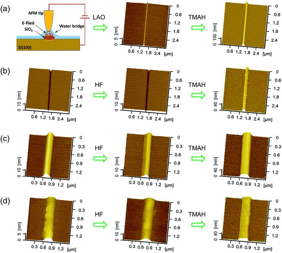 | ||
| Fig. 5 AFM images of the structures produced by friction-induced selective etching with different masks. (a) AFM images of the LAO mask before and after etching. The LAO mask was produced by a conductive tip at bias voltage of 7 V. (b) AFM images of a groove before and after etching by HF and TMAH solutions. The scratch was firstly dipped with HF solution to remove surface oxides, and then etched in TMAH solution. (c) AFM images of a protrusive hillock fabricated by selective etching at sliding speed of 10 μm s−1 (d) AFM images of a protrusive hillock fabricated by selective etching at sliding speed of 1000 μm s−1, where the wider hillock can be ascribed to the vibration in AFM scanning. In this figure, the etching time was 5 min for HF solution, and 1 min for TMAH solution, respectively. The contact pressure for the hillock formation was 5.8 GPa, and the number of scratching cycles was 100 (Fig. 5(c) and (d)). | ||
For comparison, friction-induced selective etching in TMAH solution was also conducted on Si(111) and Si(110) surfaces. Similar hillocks were produced on Si(110) surface by etching in TMAH solution (Fig. 6), while no obvious selective etching was observed on Si(111). This can be ascribed to the fact that (111) crystal plane has a very low etching rate, which is comparable to the crystal deformation mask created by scratching.28 During the etching, (111) plane played a role in preventing the etching, resulting in an inclined plane with an angle of 54.74°.
 | ||
| Fig. 6 AFM image of (a) a scratch on Si(110) and (b) a hillock produced by selective etching in TMAH for 1 min. | ||
Nanopatterning of Si surface by selective etching in TMAH solution
Friction-induced selective etching is a low-cost and flexible approach for surface patterning and fabrication. It should be noted that scanning probe microscope (SPM)-based nanofabrication by direct scratching requires a high normal load or pressure, which can cause the tip to be easily worn out, even a diamond tip. In contrast, selective etching was realized as long as the oxidation or crystal deformation occurred during scratching, and the applied normal load for scratching had minimal effect on the fabrication (Fig. 4). In other words, the fabrication by friction-induced selective etching caused less wear to the tip employed. Also, the etching with TMAH can result in high-quality surface. As shown in Fig. 7, after the same etching duration, the silicon surface after etching with TMAH solution is much smoother than that after etching with KOH. Fig. 8 presents different patterns produced on Si(100) by the friction-induced selective etching in TMAH solution, which would be helpful to produce shape-controlled patterns for optical substrates and microchannels.29–32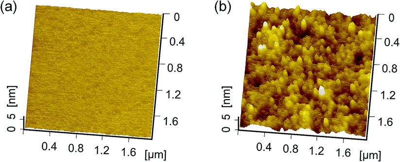 | ||
| Fig. 7 AFM images and the corresponding profiles of Si(100) surface etched by (a) TMAH and (b) KOH solutions for 5 min at 25 °C. | ||
 | ||
| Fig. 8 Nanopatterning of Si by friction-induced selective etching. | ||
When a traditional SPM scanning is employed for surface lithography, SPM tip could be easily worn due to high contact pressure for plastic deformation of substrate material during scratching.32 In contrast, high hillock or deep channels can be fabricated by friction-induced selective etching, and the process is realized at low applied load for scratching, which reduces the wear of SPM tip. It is also noted that the hillock height resulting from friction-induced selective etching is almost independent of applied load for scratching (Fig. 4), which can avoid the effect of applied load difference on fabrication results. On the other hand, any 2-dimentional surface patterns can be produced on silicon surface at low cost based on the flexibility of SPM in scanning, and it is meaningful for designing tiny channels for nanofluidics, site-controlled patterns for molecular beam epitaxy (MBE) formation of high-quality optic structures, and some functional patterns for adherent cell or bacterial analysis.29,30,33,34 As a result, the proposed study can enrich the fundamental aspects of SPM-based nanolithography, and provides an alternative method to produce nanostructures for various applications.
Experimental
Materials
P-type Si wafers, doped with boron, were purchased from MEMC Electronic Materials, Inc., USA. The surface root-mean-square (RMS) roughness was measured as about 0.10 nm over an area of 2 μm × 2 μm by an atomic force microscope (AFM; SPI3800N, Seiko Instruments Inc., Tokyo, Japan). Commercially available TMAH solution (25 wt% in water, Sinopharm Group Chemical Reagent Co., Ltd., China) was used for the etching. Before fabrication, Si wafer was cut into square shapes with a size of ∼1 cm × 1 cm. Then, the samples were dipped in 5 wt% HF solution for 5 min to etch away the native Si oxide layer for further tests.35Fabrication
The fabrication process consisted of two steps: scratching and post-etching in TMAH. The scratching was conducted by a diamond tip with a radius R of 20 nm under an applied normal load of 10 μN on AFM. The depth of these nanoscratches was 5 to 10 nm. With a diamond tip (R = 2 μm), nanoscratches were produced under continuously linear applied normal load from 0 to 6 mN on a scratcher (Ti-900, Hysitron Inc., USA). Then, the scratched Si wafers were etched in TMAH solution under specified conditions, where the temperature was controlled by a water bath thermostat with an accuracy of ±0.5 °C. Then the samples were ultrasonically washed with ethanol for 3 min, rinsed with deionized water for 3 min and dried with dry nitrogen flow in turn. Finally, the images of fabricated nanostructures were acquired in situ from the scratched area by AFM scanning with a Si3N4 tip (R ≈ 20 μm). For comparison, the selective etching of protrusive hillocks on silicon, produced by a diamond tip (R = 500 μm) on AFM, was also investigated for evaluating the etching mechanism in TMAH solution.Conclusions
In this work, the friction-induced selective etching of silicon surface in TMAH solution was investigated for fabricating nanostructures. The main conclusions of this study are summarized as follows.(1) The mechanically scratched area on silicon surface can function as a mask against etching in TMAH solution.
(2) The hillock formation by friction-induced selective etching was found to depend on the temperature and etching time. The selective etching rate increased with the temperature, while selective etching disappeared with the increase in etching time. In contrast, the applied normal load for scratching on silicon had minimal effect on the hillock height produced by selective etching in TMAH solution.
(3) In addition to silicon oxide, crystal distortions and amorphous silicon also resisted TMAH etching. Based on the proposed mechanism, a low-cost and flexible approach for patterning and fabrication of silicon surface can be realized by friction-induced selective etching.
Conflicts of interest
There are no conflicts to declare.Acknowledgements
The authors express their thanks for the financial support provided by the Sichuan Science and Technology Program (2018HH0151) and the National Natural Science Foundation of China (51775462).Notes and references
- K. Prashanthi, M. Mandal, S. P. Duttagupta, R. Pinto and V. R. Palkar, Sens. Actuators, A, 2011, 166(1), 83–87 CrossRef CAS.
- M. A. Hopcroft, W. D. Nix and T. W. Kenny, J. Microelectromech. Syst., 2010, 19(2), 229–238 CAS.
- S. Dutta, M. Imran, P. Kumar, R. Pal, P. Datta and R. Chatterjee, Microsyst. Technol., 2011, 17(10–11), 1621–1628 CrossRef CAS.
- P. Pal and K. Sato, Microsyst. Technol., 2010, 16(7), 1165–1174 CrossRef CAS.
- I. W. Rangelow, J. Vac. Sci. Technol., A, 2003, 21(4), 1550–1562 CrossRef CAS.
- M. J. De Boer, J. G. E. Gardeniers, H. V. Jansen, E. Smulders, M. J. Gilde, G. Roelofs, J. N. Sasserath and M. Elwenspoek, J. Microelectromech. Syst., 2002, 11(4), 385–401 CrossRef CAS.
- C. N. Jin, B. J. Yu, C. Xiao, L. Chen and L. M. Qian, Nanoscale Res. Lett., 2016, 11, 229 CrossRef PubMed.
- V. Swarnalatha, A. V. Narasimha Rao, A. Ashok, S. S. Singh and P. Pal, J. Micromech. Microeng., 2017, 27, 085003 CrossRef.
- R. Iosub, C. Moldovan and M. Modreanu, Sens. Actuators, A, 2002, 99(1–2), 104–111 CrossRef CAS.
- Y. Zhang, Y. Q. Zhou, Z. Y. Jiang, F. Z. Liu and M. F. Zhu, Phys. Status Solidi C, 2010, 7(3–4), 1025–1028 CAS.
- M. Shikida, K. Sato, K. Tokoro and D. Uchikawa, Sens. Actuators, A, 2000, 80(2), 179–188 CrossRef CAS.
- G. Z. Yan, P. C. H. Chan, I. M. Hsing, R. K. Sharma, J. K. O. Sin and Y. Y. Wang, Sens. Actuators, A, 2001, 89(1–2), 135–141 CrossRef CAS.
- J. Guo, C. Xiao, B. Peng and L. M. Qian, RSC Adv., 2015, 5, 100769–100774 RSC.
- J. Guo, B. J. Yu, L. Chen and L. M. Qian, Sci. Rep., 2015, 5, 16472 CrossRef CAS PubMed.
- J. Guo, C. F. Song, X. Y. Li, B. J. Yu, H. S. Dong, L. M. Qian and Z. R. Zhou, Nanoscale Res. Lett., 2012, 7, 152 CrossRef PubMed.
- C. F. Song, B. J. Yu and L. M. Qian, Micro Nano Lett., 2013, 8(10), 735–739 CrossRef CAS.
- C. F. Song, X. Y. Li, S. X. Cui, H. S. Dong, B. J. Yu and L. M. Qian, Nanoscale Res. Lett., 2013, 8, 140 CrossRef PubMed.
- C. F. Song, B. J. Yu, M. Wang and L. M. Qian, RSC Adv., 2015, 5(97), 79964–79968 RSC.
- J. Guo, B. J. Yu, X. D. Wang and L. M. Qian, Nanoscale Res. Lett., 2014, 9, 241 CrossRef PubMed.
- P. Tang, B. J. Yu, J. Guo, C. F. Song and L. M. Qian, Nanoscale Res. Lett., 2014, 9, 59 CrossRef PubMed.
- B. J. Yu, H. S. Dong, L. M. Qian, Y. F. Chen, J. X. Yu and Z. R. Zhou, Nanotechnology, 2009, 20, 465303 CrossRef PubMed.
- B. J. Yu, H. T. He, L. Chen and L. M. Qian, Wear, 2017, 374, 29–35 CrossRef.
- B. J. Yu, L. M. Qian, H. S. Dong, J. X. Yu and Z. R. Zhou, Wear, 2010, 268(9–10), 1095–1102 CrossRef CAS.
- J. S. You, D. Kim, J. Y. Huh, H. J. Park, J. J. Pak and C. S. Kang, Sol. Energy Mater. Sol. Cells, 2001, 66(1–4), 37–44 CrossRef CAS.
- D. Stiévenard and B. Legrand, Prog. Surf. Sci., 2006, 81, 112–140 CrossRef.
- B. J. Yu, X. Y. Li, H. S. Dong, Y. F. Chen, L. M. Qian and Z. R. Zhou, J. Phys. D: Appl. Phys., 2012, 45, 145301 CrossRef.
- L. Chen, J. L. Wen, P. Zhang, B. J. Yu, C. Chen, T. B. Ma, X. C. Lu, S. H. Kim and L. M. Qian, Nat. Commun., 2018, 9, 1542 CrossRef PubMed.
- C. N. Jin, B. J. Yu, X. X. Liu, C. Xiao, H. B. Wang, S. L. Jiang, J. Wu, H. Y. Liu and L. M. Qian, Appl. Surf. Sci., 2017, 425, 227–232 CrossRef CAS.
- W. sparreboom, d. B. A. Van and J. C. eijkel, Nat. Nanotechnol., 2009, 4, 713 CrossRef CAS PubMed.
- X. Y. Chen and L. Zhang, Sens. Actuators, B, 2017, 254, 648–659 CrossRef.
- A. Krost and A. Dadgar, Mater. Sci. Eng., B, 2002, 93(1–3), 77–84 CrossRef.
- A. G. Khurshudov, K. Kato and H. Koide, Tribol. Lett., 1996, 2(4), 345–354 CrossRef CAS.
- J. Norman, M. J. Kennedy, J. Selvidge, Q. Li, Y. Wan, A. Y. Liu, P. G. Callahan, M. P. Echlin, T. M. Pollock, K. M. Lau, A. C. Gossard and J. E. Bowers, Opt. Express, 2017, 25(4), 3927–3934 CrossRef CAS PubMed.
- C. Berne, C. K. Ellison, A. Ducret and Y. V. Brun, Nat. Rev. Microbiol., 2018, 10(16), 616–627 CrossRef PubMed.
- G. R. Guo, J. M. Li, C. B. Deng, Q. P. He, Q. Y. Yu, C. Zhou, X. X. Liu, S. L. Jiang, L. Chen, B. Y. Yu and L. M. Qian, Appl. Phys. Express, 2018, 11, 116501 CrossRef.
| This journal is © The Royal Society of Chemistry 2018 |