
 Open Access Article
 This Open Access Article is licensed under a Creative Commons Attribution-Non Commercial 3.0 Unported Licence
Solution-processed amorphous ZrO2 gate dielectric films synthesized by a non-hydrolytic sol–gel route†
Jong-Baek Seona,
Nam-Kwang Cho a,
Gayeong Yooa,
Youn Sang Kim*ab and
Kookheon Char*c
a,
Gayeong Yooa,
Youn Sang Kim*ab and
Kookheon Char*c
aProgram in Nano Science and Technology, Graduate School of Convergence Science and Technology, Seoul National University, Seoul 08826, Republic of Korea. E-mail: younskim@snu.ac.kr
bAdvanced Institutes of Convergence Technology, 864-1 Iui-dong, Yeongtong-gu, Suwon-si, Gyeonggi-do 16229, Republic of Korea
cSchool of Chemical & Biological Engineering, Seoul National University, Seoul 08826, Republic of Korea. E-mail: khchar@snu.ac.kr
First published on 22nd November 2018
Abstract
Solution-processed zirconium oxide (ZrO2) dielectrics were formed via a non-hydrolytic sol–gel route at low-temperature, and are suitable for flexible thin film transistor (TFT) devices. Precursor solutions with equimolar zirconium halide and zirconium alkoxide were prepared, and amorphous ZrO2 films were obtained by spin-coating and annealing at 300 °C through the direct condensation reaction between them. The ZrO2 films exhibited a high dielectric constant near 10, and a low leakage current density of 5 × 10⁻⁸ A cm−2 at a field of 1 MV cm−1. High mobility p-type pentacene TFTs were fabricated using the ZrO2 dielectrics, with a saturation field-effect mobility of 3.7 cm2 V−1 s−1, a threshold voltage of −2.7 V, an on/off ratio of 1.1 × 10⁶ and a subthreshold swing of 0.65 V dec−1.
High dielectric constant (high-k) materials have received great interest as alternatives to conventional dielectric materials such as silicon dioxide (SiO2). These high-k dielectrics can be used as key components of the semiconductor and display industry in the form of capacitor dielectrics and transistor gate insulators.1 In the semiconductor industry, as the traditional gate dielectric becomes extremely thin (∼a few atomic layer thick), leakage currents are generated due to direct tunneling of electrons through the dielectric itself, resulting in power dissipation and heat emission, which is a serious problem to be solved. High-k dielectrics are expected to reduce the leakage currents since thicker dielectric layers can be used without altering the required dielectric properties.1,2 In the display industry, high-k dielectrics are considered core materials that allow high on-currents in low voltage operation resulting in low-power consumption devices. Among many high-k materials, zirconium oxide (ZrO2) was chosen because of its outstanding physical and chemical properties such as high intrinsic dielectric constants, high melting points, and great chemical stability.3 ZrO2 is an important metal oxide and has been applied to several technologies including gate dielectrics.2–4
Compared with vacuum-based processes such as chemical vapor deposition (CVD) and sputtering, solution-based processes (especially sol–gel methods) have distinguished advantages: low-cost and ease of large area deposition. However, solution-processes based on conventional hydrolytic sol–gel methods involve hydrolysis and condensation reactions, which require high thermal energy to form three-dimensional solid networks of pure components.5 In the past, several groups have reported on the synthesis of inorganic oxides via non-hydrolytic sol–gel routes.6–12 The basis of these methods is the reaction between a metal halide and an oxygen donor in the absence of water. The oxygen donor may be an alkoxide, an ether or an alcohol. The reaction formulae using an alkoxide or an ether as an oxygen donor are as follows.8–12
| MXn + M(OR)n → 2MOn/2 + nRX (alkoxide route) | (1) |
| MXn + (n/2)ROR → MOn/2 + nRX (ether route) | (2) |
In the above reaction scheme, the ether route is finally followed by the alkoxide route, in which the alkoxide generation is preceded by a substitution reaction between an alkoxide and an ether.
![[triple bond, length as m-dash]](https://www.rsc.org/images/entities/char_e002.gif) M–X + R–O–R → M–OR + R–X M–X + R–O–R → M–OR + R–X
| (3) |
Finally, the metal oxide network formation is completed through the condensation reaction between the metal halide and the alkoxide as described in eqn (1).
By direct condensation without any hydroxylation of the conventional hydrolytic sol–gel route, the above reactions complete at lower temperatures than the hydrolytic ones.12 The advantages of low temperature process are variously known, including flexible and low-cost processes. The most important characteristic we thought of is the ability to form amorphous films. Amorphous gate insulators are generally preferred because of their smooth surfaces, which eliminates some of problems associated with grain boundaries in crystalline films. The crystalline rough surfaces induce charge trapping and leakage currents, deteriorating the channel mobility and the reliability of thin film devices.13–16 Even though ZrO2 crystallizes at much lower temperatures than SiO2,2 the crystallinity of thin ZrO2 films can be controlled by adjusting the process temperature of the non-hydrolytic sol–gel method.
In this letter, we present the solution-processed amorphous ZrO2 thin films by a non-hydrolytic sol–gel route that can be applied as gate insulators for TFTs. To demonstrate advantages of the high dielectric quality of the ZrO2 films, we selected a pentacene as channel material for TFT devices. Pentacene was thermally evaporated, which minimizes secondary effects that may influence the properties of the gate insulator, either chemically or thermally. To grow the ZrO2 thin films, the precursor solution was spin-coated onto Si wafers and glass substrates and then annealed at low temperature (∼300 °C). Also, to investigate the physical properties of the thin ZrO2 films including morphological and electrical characteristics, we carried out several analyses, such as X-ray diffraction (XRD), scanning electron microscopy (SEM), current–voltage (IV) and TFT characterization. The ZrO2 films exhibited a high dielectric constant near 10 and p-type pentacene TFTs with high mobility were fabricated using the ZrO2 dielectrics, with a saturation field-effect mobility of 3.7 cm2 V−1 s−1.
Materials such as zirconium(IV) isopropoxide isopropanol complex (Zr[OCH(CH3)2]4(CH3)2CHOH), zirconium(IV) chloride (ZrCl4) and 2-methoxy ethanol were used as received without further purification. We prepared equimolar amounts of ZrCl4 and Zr[OCH(CH3)2]4(CH3)2CHOH precursor solutions with concentrations of 5 wt% and 16 wt% in 2-methoxyethanol respectively. The prepared solutions were then spin-coated onto silicon and glass substrates at 500 rpm. Finally, the coated substrates were baked at 100 °C on a hot plate for 1 min for solvent evaporation and then post-annealed at 300 °C and 400 °C on a hot plate and 600 °C in a furnace for 1 h for the curing of the thin films to confirm their morphology at each temperature.
To study the electrical properties of the ZrO2 thin films, we fabricated metal–insulator–metal (MIM) structures (Fig. 1(a)). The dielectric constants, the leakage currents, and the breakdown voltages of the ZrO2 thin films were measured. TFT devices were also fabricated as shown in Fig. 1(b) to investigate the high-k effect of ZrO2 gate dielectrics with pentacene channel layers. Pentacene channel layers were deposited by thermal evaporation. In both devices, we used shadow masks for patterning aluminum (Al) top electrodes, pentacene channel layer, and gold (Au) source/drain electrodes. In the TFT device structure, molybdenum/tungsten alloy (MoW) gate electrodes were patterned by photolithographic processes.
 | ||
| Fig. 1 (a) Metal–insulator–metal (MIM) structure used to measure the dielectric constants, the leakage currents, and the breakdown voltages of the ZrO2 films (Al diameter = 1 mm). (b) TFT structure with a 700 Å pentacene channel and a 1500 Å ZrO2 gate dielectric layer (L (channel length) = 160 μm; W (channel width) = 1 mm). | ||
The thickness of ZrO2 thin films were measured with a spectroscopic ellipsometer (M-2000V, J. A. Woollam. Co. Inc.). The film crystallinity was measured at 40 kV and 30 mA using a Phillips X'pert Pro X-ray diffractometer equipped with a Cu Kα source. The surface morphology were measured using a Hitachi S4800 scanning electron microscopy. The dielectric constants of ZrO2 thin films were measured using an Agilent 4284A precision LCR meter in the frequency range between 20 Hz and 100 kHz. Leakage currents, breakdown voltages and TFT characteristics were measured by a Keithley 4200, semiconductor characterization system.
Through the spin-coating and annealing process, we have obtained thin ZrO2 films by the non-hydrolytic sol–gel route. The film thicknesses were 420 Å and 1500 Å with concentration of 5 wt% and 16 wt%, respectively. We chose the alkoxide route mentioned in reaction (1), where zirconium chloride and zirconium isopropoxide act as a metal halide and a metal alkoxide (an oxygen donor), respectively. XRD and SEM analyses were performed to confirm the possibility of controlling the film morphology by varying the annealing temperature. Fig. 2 shows the X-ray diffraction patterns of the thin ZrO2 films with post-annealing temperatures of 300 °C, 400 °C, and 600 °C. An amorphous phase is observed for the samples with 300 °C and 400 °C. Only the sample annealed at 600 °C exhibits a crystalline structure. ZrO2 exists in three major crystal phases: cubic, tetragonal, and monoclinic polymorphs.17 In our experiment, the thin films annealed at 600 °C showed the tetragonal phase. From the full width at half maximum height of the peak, the crystalline domain size can be estimated by the Scherrer relation (Ls = nλ/β![[thin space (1/6-em)]](https://www.rsc.org/images/entities/char_2009.gif) cosθ, where n is unity, λ the wavelength of incident X-rays and θ the diffracted angle). The crystalline domain size was calculated to be about 160 Å, which means that grain boundaries are caused by the nanocrystals in the amorphous matrix. Through SEM analysis (Fig. S1†), the morphology of the thin film surface could be confirmed intuitively, and a comprehensive conclusion could be made comparing with the crystallographic analysis of XRD. As expected, the conditions of 300 °C and 400 °C show microscopically flat surfaces, and at 600 °C, it is a rough surface due to the crystal growth as confirmed by XRD. To avoid deleterious effects of the grain boundaries and take advantage of the various features of the low temperature processes, we adopted the low temperature processed (∼300 °C) films as gate insulators for TFTs fabrication. In addition, because of the tendency of binary oxides to crystallize at low thermal energy, multi-metal oxides are commonly used to induce amorphous structures.13 One of the important facts to consider in this work is that reliable amorphous gate insulators can be obtained using only binary oxides at relatively low temperatures by virtue of the non-hydrolytic sol–gel route.
cosθ, where n is unity, λ the wavelength of incident X-rays and θ the diffracted angle). The crystalline domain size was calculated to be about 160 Å, which means that grain boundaries are caused by the nanocrystals in the amorphous matrix. Through SEM analysis (Fig. S1†), the morphology of the thin film surface could be confirmed intuitively, and a comprehensive conclusion could be made comparing with the crystallographic analysis of XRD. As expected, the conditions of 300 °C and 400 °C show microscopically flat surfaces, and at 600 °C, it is a rough surface due to the crystal growth as confirmed by XRD. To avoid deleterious effects of the grain boundaries and take advantage of the various features of the low temperature processes, we adopted the low temperature processed (∼300 °C) films as gate insulators for TFTs fabrication. In addition, because of the tendency of binary oxides to crystallize at low thermal energy, multi-metal oxides are commonly used to induce amorphous structures.13 One of the important facts to consider in this work is that reliable amorphous gate insulators can be obtained using only binary oxides at relatively low temperatures by virtue of the non-hydrolytic sol–gel route.
 | ||
| Fig. 2 XRD patterns of the spin-coated thin ZrO2 films post-annealed at 300 °C, 400 °C, and 600 °C, respectively. | ||
In order to investigate the potential of thin ZrO2 films as gate insulators of TFTs, the dielectric constants, the leakage currents, and the breakdown voltages of the ZrO2 thin films were measured. Fig. 3(a) shows the measured dielectric constants of a ZrO2 film over the predetermined frequency range, indicating a high dielectric constant of about 10 at 100 kHz. This value is generally less than the known value, over 20.2–4 Our solution-processed thin ZrO2 films are amorphous and inevitably contain pores as a consequence of the sol–gel process.5 This, in turn, produces a film of lower density than a vacuum-deposited crystalline film, and as a result the dielectric constant of the film must be small. Even though the non-hydrolytic sol–gel ZrO2 films have relatively small dielectric constants compared to their vacuum deposited counterparts, the amorphous nature could offset this negative effect by minimizing the grain boundary-induced device instability, and they still have a much higher dielectric constant value than silicon dioxide (∼3.9). Fig. 3(b) shows the leakage current characteristics of the ZrO2 films. The leakage current at an electric field of 1 MV cm−1 is observed at about 5 × 10⁻⁸ A cm−2 and the breakdown voltage is greater than 4 MV cm−1, which demonstrates the applicability of gate dielectrics. Besides, the completion of the ZrO2 non-hydrolytic sol–gel reaction at a temperature of 300 °C or higher can also be confirmed by the electrical characteristics at 300 °C. Similar dielectric constants were measured according to frequencies. Generally, when the reaction is insufficient, abnormal dielectric constant values appear at high frequencies due to the mobile charges in the films. In addition, low leakage currents also represent a stable ZrO2 thin film state.
For the pentacene TFT, a representative output curve of the drain current (IDS) versus the drain voltage (VDS) at various gate voltages (VGS) is shown in Fig. 4(a). The TFT demonstrates a typical transistor behaviour. Current saturation is observed at high VDS as the accumulation layer of the pentacene channel is pinched off near the drain electrode. A transfer curve of IDS versus VGS with a VDS of −10 V is plotted in Fig. 4(b). By taking the square root of both sides in the following equation, TFT characteristics including the field effect mobility (μ) were obtained in the saturation regime.18
 | (4) |
:H) TFT modeling.22–24 Lee et al. have demonstrated the same relevance for oxide semiconductor TFTs using the MTR model and noted generalization for disordered semiconductor TFTs including the organic TFTs.25 They modelled the relationship between mobility and capacitance and presented a generalized equation.25 Another remarkable feature of our results is a very small subthreshold swing. It determines the voltage swing required to switch the device from the “off” to “on” state. The small subthreshold swing allows TFTs with low operating voltage to be implemented.
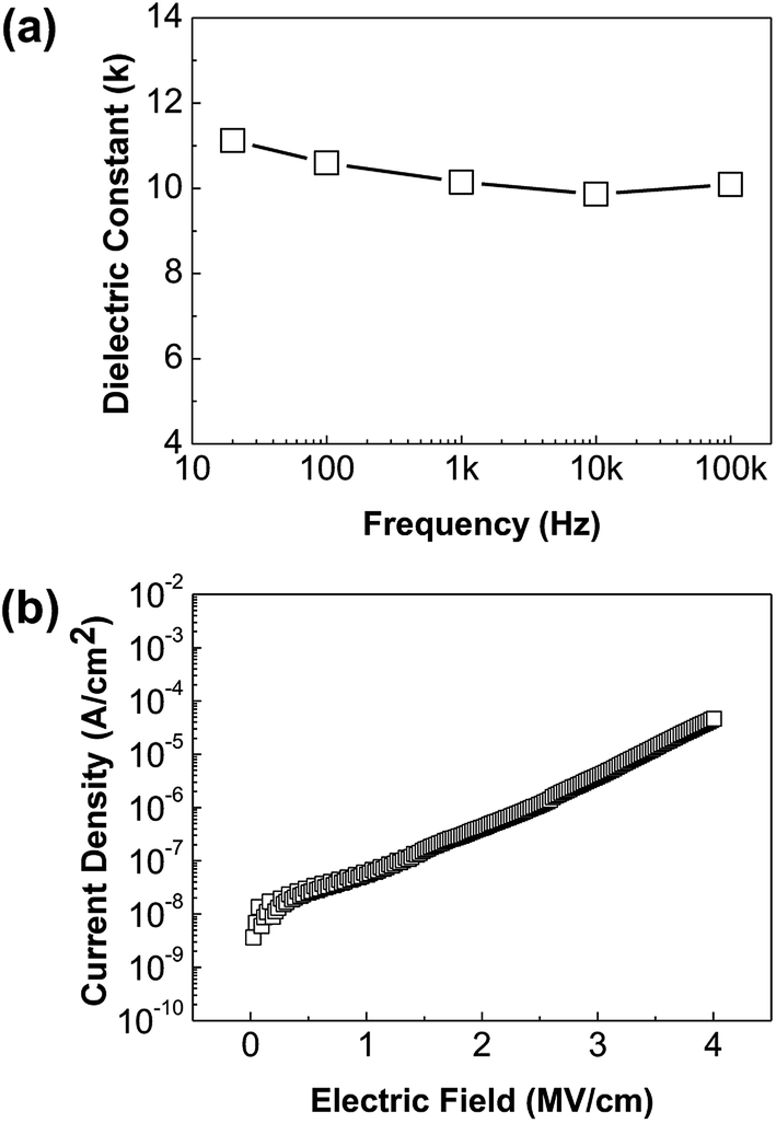 | ||
| Fig. 3 (a) Dielectric constants of a thin ZrO2 films as a function of frequency, (b) leakage current across a thin ZrO2 film. | ||
 | ||
| Fig. 4 Device characteristics of spin-coated ZrO2/pentacene TFT devices. (a) Output characteristics: VGS varied from 0 V to −8 V, (b) Transfer characteristics: VDS = −10 V. | ||
Conclusions
In summary, we have demonstrated the potential of solution-processed amorphous ZrO2 high-k dielectric films fabricated with a non-hydrolytic sol–gel route at low temperature to realize high-performance devices at low voltage. We have succeeded in fabricating spin-coated ZrO2 thin films using a non-hydrolytic sol–gel route and demonstrated through chemical reactions that this is possible and have opened up a new way to develop high-k dielectrics at low process temperatures (∼300 °C). In spite of amorphous ZrO2, a dielectric constant near 10 and a low leakage current density of 5 × 10⁻⁸ A cm−2 at a field of 1 MV cm−1 were obtained. Besides, TFTs with these ZrO2 gate dielectrics showed excellent transistor characteristics: the field-effect mobility at the saturation region of 3.7 cm2 V−1 s−1 and the subthreshold swing of 0.65 V dec−1, which is critical in low voltage operation. In these results, the potential of non-hydrolytic sol–gel ZrO2 high-k dielectrics for the enhancement of TFT device performance was successfully demonstrated.Conflicts of interest
There are no conflicts of interest to declare.Acknowledgements
This work was supported by Samsung Advanced Institute of Technology.Notes and references
- A. I. Kingon, J.-P. Maria and S. K. Streiffer, Nature, 2000, 406, 1032 CrossRef CAS PubMed.
- J. Robertson, Rep. Prog. Phys., 2006, 69, 327 CrossRef CAS.
- J. Tang, J. Fabbri, R. D. Robinson, Y. Zhu, I. P. Herman, M. L. Steigerwald and L. E. Brus, Chem. Mater., 2004, 16, 1336 CrossRef CAS.
- G. D. Wilk, R. M. Wallace and J. M. Anthony, J. Appl. Phys., 2001, 89, 5243 CrossRef CAS.
- J.-B. Seon, S. Lee, J. M. Kim and H.-D. Jeong, Chem. Mater., 2009, 21, 604 CrossRef CAS.
- S. Acosta, P. Arnal, R. J. P. Corriu, D. Leclercq, P. H. Mutin and A. Vioux, Mater. Res. Soc. Symp. Proc., 1994, 346, 43 CrossRef CAS.
- R. J. P. Corriu, D. Leclercq, P. Lefevre, P. H. Mutin and A. Vioux, J. Non-Cryst. Solids, 1992, 146, 301 CrossRef CAS.
- P. Arnal, R. J. P. Corriu, D. Leclercq, P. H. Mutin and A. Vioux, Chem. Mater., 1997, 9, 694 CrossRef CAS.
- M. Andrianainarivelo, R. J. P. Corriu, D. Leclercq, P. Lefevre, P. H. Mutin and A. Vioux, J. Sol-Gel Sci. Technol., 1997, 8, 89 CAS.
- J. N. Hay and H. M. Raval, J. Mater. Chem., 1998, 8, 1233 RSC.
- J. N. Hay and H. M. Raval, J. Sol-Gel Sci. Technol., 1998, 13, 109 CrossRef CAS.
- J. N. Hay, D. Porter and H. M. Raval, J. Mater. Chem., 2000, 10, 1811 RSC.
- J. F. Wager, D. A. Keszler, and R. E. Presley, Transparent Electronics, Springer, New York, 2008 Search PubMed.
- H. Kim, Y.-J. Kwack, E.-J. Yun and W.-S. Choi, Sci. Rep., 2016, 6, 33576 CrossRef CAS PubMed.
- H. Tan, G. Liu, A. Liu, B. Shin and F. Shan, Ceram. Int., 2015, 41, S349 CrossRef CAS.
- P. Barquinha, L. Pereira, G. Goncalves, R. Martins, D. Kuscer, M. Kosec and E. Fortunato, J. Electrochem. Soc., 2009, 156, H824 CrossRef CAS.
- J. Joo, T. Yu, Y. W. Kim, H. M. Park, F. Wu, J. Z. Zhang and T. Hyeon, J. Am. Chem. Soc., 2003, 125, 6553 CrossRef CAS PubMed.
- C. R. Kagan and P. Andry, Thin-Film Transistors, Marcel Dekker, New York, 2003 Search PubMed.
- D. K. Hwang, K. Lee, J. H. Kim and S. Im, Appl. Phys. Lett., 2006, 89, 093507 CrossRef.
- S. M Sze and K. K. Ng, Physics of Semiconductor Devices, Wiley, Hoboken, 2007 Search PubMed.
- C. D. Dimitrakopoulos, S. Purushothaman, J. Kymissis, A. Callegari and J. M. Shaw, Science, 1999, 283, 822 CrossRef CAS PubMed.
- C. D. Dimitrakopoulos, I. Kymissis, S. Purushothaman, D. A. Neumayer, P. R. Duncombe and R. B. Laibowitz, Adv. Mater., 1999, 11, 1372 CrossRef CAS.
- S. Lee, D.-J. Yun, S.-W. Rhee and K. Yong, J. Mater. Chem., 2009, 19, 6857 RSC.
- P. G. Le Comber and W. E. Spear, Phys. Rev. Lett., 1970, 25, 509 CrossRef CAS.
- E. Lee, J. Ko, K.-H. Lim, K. Kim, S. Y. Park, J. M. Myoung and Y. S. Kim, Adv. Funct. Mater., 2014, 24, 4689 CrossRef CAS.
Footnote |
| † Electronic supplementary information (ESI) available. See DOI: 10.1039/c8ra06911e |
| This journal is © The Royal Society of Chemistry 2018 |