
 Open Access Article
 This Open Access Article is licensed under a Creative Commons Attribution-Non Commercial 3.0 Unported Licence
Highly intense room-temperature photoluminescence in V2O5 nanospheres
Top Khac Lea,
Manil Kang *b,
Sang Wook Hana and
Sok Won Kim*a
*b,
Sang Wook Hana and
Sok Won Kim*a
aDepartment of Physics, University of Ulsan, Ulsan 44610, Republic of Korea. E-mail: sokkim@ulsan.ac.krb
bDepartment of Physics, Kongju National University, Kongju 32588, Republic of Korea. E-mail: ifriver@kongju.ac.kr
First published on 11th December 2018
Abstract
Room-temperature photoluminescence (PL) in V2O5 nanospheres with zero-like dimensional structure was investigated. A large number of V4+ oxidation states in the nanospheres were observed by X-ray photoelectron spectroscopy (XPS) measurements. The nanospheres revealed high PL intensity compared with previous studies. In particular, they showed intense ultraviolet (UV) PL near a wavelength of 396 nm (3.13 eV). The intense UV PL was attributed to the enhanced transition probability due to the large number of V4+ (3d1) oxidation states. The PL properties showed strong dependencies on the oxidation states and their distribution.
1. Introduction
Vanadium pentoxide (V2O5) is very stable and has notable applications in chemical sensing, catalysis, Li-ion intercalation, and visible photoluminescence (PL).1–4 Much effort has been devoted to improving these promising properties, and the synthesis of nanostructures has drawn much attention. Thin-film V2O5 shows visible PL due to band-edge transitions and defects, but its emission intensity is very weak at room temperature. To enhance the PL intensity, various nanostructures have been grown, such as nanorods, nanowires, and nanoparticles.5–7 Previous studies have reported the synthesis of V2O5 nanostructures and enhanced visible PL. The reported V2O5 nanostructures show a weak and broad emission centred at ∼530 nm (2.34 eV) due to the band edge transition and centred at ∼710 nm (1.74 eV), which is attributed to mid-gap states (∼1.84 eV) formed by oxygen defects that occurred during growth.8–10 This result may be due to their growth structure. Most nanoparticles and nanorods are attached to each other, and their growth length is also short. The attachment and small growth size of the nanoparticles and nanorods allows them to form many interfaces between them, and the interfaces can promote the separation of photogenerated carrier pairs, which reduces the radiative recombination rate. However, Hu et al. reported intense room-temperature PL near 700 nm in V2O5 nanorods with a length of ∼2 μm.9 This result may indicate that intense room-temperature PL can be obtained in micro-length nanorods. Therefore, The PL intensity in V2O5 nanostructures strongly depends on the synthesis method and microstructure. Enhanced PL properties could make V2O5 a promising material for applications in indicators and light sources.Micro- and nano-sized V2O5 spheres have also been studied as cathode materials for Li-ion batteries to achieve high capacity and high output voltage.11,12 However, other properties have received less attention, including catalysis, photochromism, and visible PL in V2O5 with spherical structures. One-dimensional structures such as nanorods and nanowires show superior PL properties to two-dimensional structures (thin films). The investigation of nanospheres (which have zero-like dimensional structure) is very important for the development of optical devices.
We report on the synthesis of V2O5 nanospheres and their PL properties at room temperature. The microstructure and oxidation state of the nanospheres were investigated, and PL measurements were performed at room temperature. Also, the PL mechanism in the nanospheres was discussed.
2. Experimental section
Preparation of V2O5 nanospheres
V2O5 nanospheres were synthesized by a chemical reaction method.11 NH4VO3 of 0.234 g was dissolved in distilled water of 90 mL and stirred for 1 h. Then, 1 M HCl solution of 1 mL was dropped into the solution and stirred for 30 min before adding hydrazine NH4·H2O of 3 mL, followed by stirring for 10 min at room temperature. The resulting V(OH)2NH2 nanospheres were filtered and washed several times with deionized water and then dried at 80 °C for 6 h. The precursor was dispersed in deionized water and then spin-coated on a quartz substrate at a speed of 3000 rpm for 1 minute. Finally, to obtain V2O5 nanospheres, the coated precursor was calcined using a tubular furnace at 350 °C in air for 2 h.Structure characterization
The morphology of the nanospheres was investigated using high-resolution scanning electron microscopy (HR FE-SEM, Mira LMH, Tescan) and transmission electron microscopy (TEM, H-8100, Hitachi). The crystal structure was characterized using an X-ray diffractometer (XRD, DMax 2000, Rigaku) with Cu Kα radiation, as well as a Raman/PL spectrometer (Horiba-Jobin Yvon, LabRAM HR) equipped with a He–Ar laser at a wavelength of 514.5 nm.Characterization
X-ray photoelectron spectroscopy (XPS) measurements were performed to investigate the oxidation states of the nanospheres. The XPS spectra were recorded with a Thermo-Scientific MultiLab ESCA 2000 system equipped with a 300 W Mg Kα source. The C1s, O1s, and V2p core levels were measured. When fitting the V2p and O1s core-level spectra, the Gaussian width was fixed at the instrumental resolution of 0.75 eV. For curve-fitting of the V2p peaks, the values of the spin–orbit splitting and the branching ratios [I(2p3/2)/I(2p1/2)] were fixed at 7.6 eV and 0.5, respectively.PL measurements were performed at room temperature using a Raman/PL spectrometer (Horiba-Jobin Yvon, LabRAM HR) equipped with a He–Cd laser with a wavelength of 325 nm and a maximum power of 200 mW. Time-resolved PL (TRPL) measurements were performed using an inverted scanning confocal microscope (MicroTime-200, Picoquant). A single-mode pulsed diode laser (LDH-P-C-375, Picoquant) with a pulse width of ∼30 ps was used as an excitation source. The time-correlated single-photon counting (TCSPC) technique was used to count the PL photons. TRPL images with dimensions of 200 × 200 pixels were recorded using the time-tagged time-resolved (TTTR) data acquisition method. The acquisition time of each pixel was 1 ms.
3. Results and discussion
Fig. 1(a) and (b) show the morphology and a histogram of V2O5 nanospheres obtained from SEM measurements. The size distribution of the nanospheres was evaluated using the histogram, which has a Gaussian profile. To obtain the size distribution, we used the ImageJ program. The size of individual nanosphere in SEM image was calculated by using the program. The SEM image and histogram reveal that the nanospheres have a diameter of 284 ± 22 nm, spherical morphology, and numerous defects on their surfaces. These defects are due to the growth feature of α-V2O5 with a layer-by-layer (plate-like) structure. V2O5 nanospheres grown in this study have a crystal structure of α-V2O5. Initially, V2O5 is grown to a layer (or plate) structure. As time passes, the number of layer increases. Simultaneously, edges of the plate structure are etched by solution. Due to the process, the layer-by-layer structure changes to sphere structure, and numerous defects are formed on surface of sphere.13,14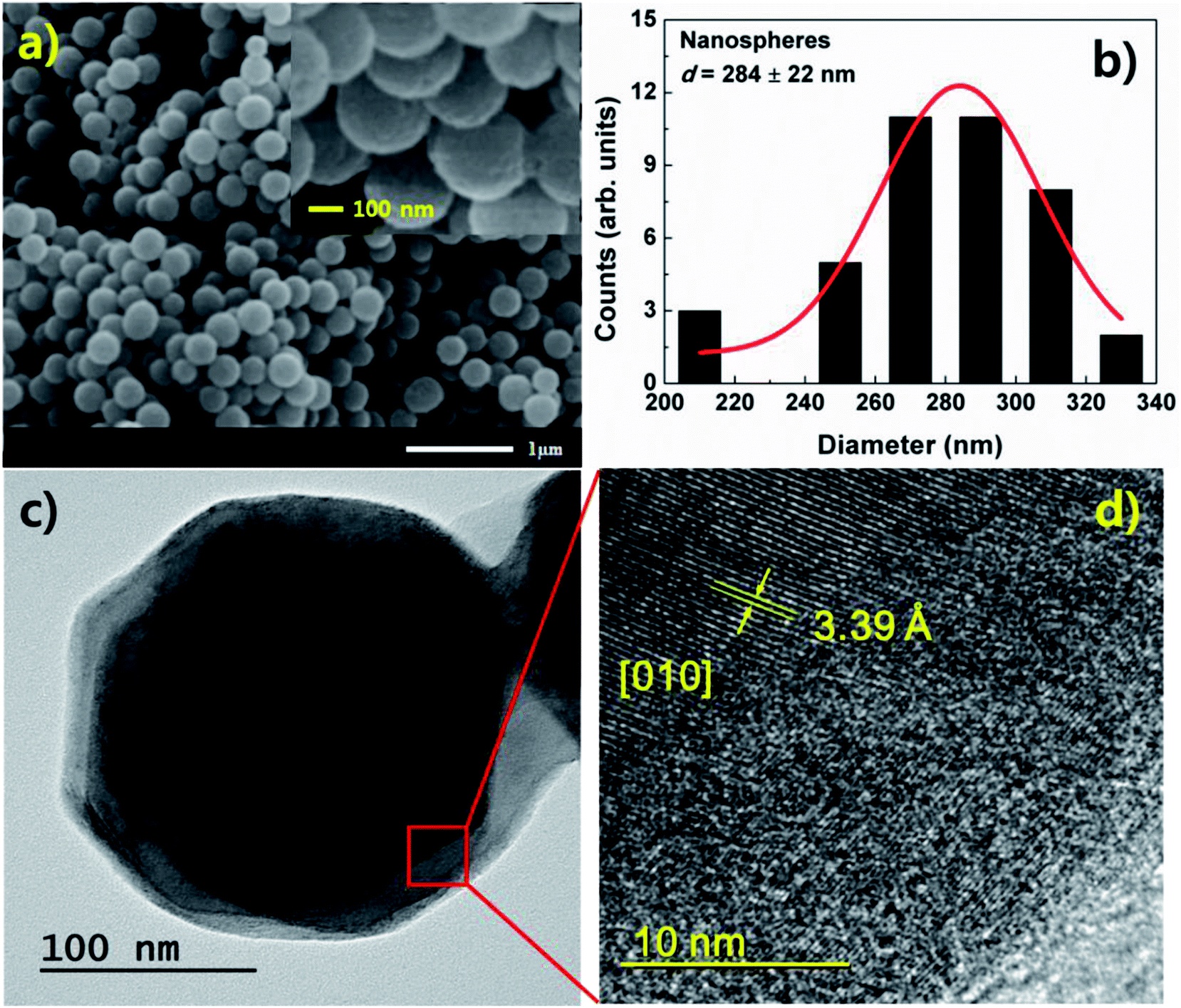 | ||
| Fig. 1 (a) SEM image and (b) histogram of V2O5 nanospheres. (c) TEM image of the nanospheres showing the solid sphere structure. (d) High-resolution TEM image with atomic array of V2O5 observed at center of the nanosphere. | ||
A TEM image of the nanospheres is shown in Fig. 1(c). The image shows solid sphere structures. Fig. 1(d) shows a high-resolution TEM image. An atomic array of V2O5 is observed at the center of the sphere, indicating high crystallinity. On the surface, the atomic array becomes disordered due to the etching, implying poor crystallinity and the formation of numerous defects. In the observed region, a lattice parameter of b = 3.39 Å for α-V2O5 was obtained from the TEM image (Fig. 1(d)). The center of the sphere shows a preferential [010] orientation.
Fig. 2(a) shows the XRD pattern of the nanospheres, where there is a diffraction peak corresponding to the (001) plane of α-V2O5 at 20.3° (JCPDS 01-077-2418).8–10 Additional peaks corresponding to the (200), (101), (110), and (301) planes are also observed. This result indicates that the nanosphere has polycrystalline structure. Furthermore, the pattern shows unidentified peaks. The existence of unidentified peaks implies that the V2O5 nanosphere includes other phases of vanadium oxide. The measured Raman spectra are presented in Fig. 2(b). The spectra reveal the typical Raman-active mode of α-V2O5.15,16 The results in Fig. 2(a) and (b) indicate that the nanospheres contain the α-V2O5 phase.
 | ||
| Fig. 2 (a) XRD pattern and (b) Raman spectrum of V2O5 nanospheres. (c) XPS spectrum of the nanospheres. The V2p and O1s core-level spectra shift toward lower binding energy, and the peak at 532.2 eV originated from the SiO2 substrate. | ||
Fig. 2(c) shows the XPS spectra of the nanospheres. The V2p and O1s core-level spectra of the nanospheres shift toward lower binding energy with the appearance of an additional oxygen peak at higher binding energy, which are attributed to the SiO2 substrate. A deconvolution fit indicates that the V2p peak (p3/2) of the nanospheres mainly consists of the V4+ oxidation state (516.1 eV). The energy of the peak is very small (0.8 eV) compared with the V5+ oxidation state (516.9 eV) corresponding to the α-V2O5 phase.17–19 This result implies that the states are oxidized into a lower oxidation state. Furthermore, the peak maxima of the O1s core-level spectra shifts to lower energy for the nanospheres. The stoichiometry ratios (Sij) of the nanospheres are calculated from the XPS spectra using the following formula: Sij = Ci/Cj = (Ii/ASFi)/(Ij/ASFj), where, Ci and Cj are the concentrations of the elements, Ii and Ij the background corrected intensities of the photoelectron emission lines and ASFi and ASFj the atomic sensitivity factors for photoionization of the ith and jth elements. For example, ASFO and ASFV are 2.93 and 9.66, which are supplied with the instrument.20 The O/V rate of the nanospheres is 3.04, while the amount of V4+ in the V2p peak is 84%.
Fig. 3(a) presents the PL spectra of phase nanospheres measured at room temperature. The nanospheres exhibit highly intense PL with three main peaks. The PL peak centered at ∼530 nm (2.34 eV) is due to the band edge transition in V2O5 with a bandgap energy of 2.3–2.4 eV.21,22 Another PL peak centered at ∼710 nm (1.74 eV) is attributed to mid-gap states (∼1.84 eV) formed by oxygen defects that occurred during growth.9,10 The nanospheres show an intense UV PL peak centered at ∼396 nm (3.13 eV), which has not been reported previously. This peak is considered to be due to strong UV absorption resulting from the large amount of V4+ oxidation states in the nanospheres (Fig. 2(c)), which can be strongly excited by UV light with wavelength in the range of 250–350 nm.23 Meyn et al. investigated the PL properties of V4+-doped oxides such as Al2O3 and YAlO3 and reported that the UV light absorption in the oxides can be enhanced by V4+.
 | ||
| Fig. 3 (a) Room-temperature PL spectrum in V2O5 nanospheres. (b) PL spectra with distribution of the nanospheres and (Inset) SEM image. (c) SEM images and (d) PL spectra with respect to spin-coating frequency of the nanospheres. | ||
The V5+ and V4+ oxidation states have valence-electron configurations of V 3d0 and V 3d1 in the valence band,24,25 respectively. The binding energy (516.1 eV) of the nanospheres with a dominant V4+ oxidation state decreases to 0.8 eV, which is small compared with that of α-V2O5 (516.9 eV) with a dominant V5+ oxidation state. The 3d1 valence-electron configuration and the lower binding energy of the V4+ oxidation state can significantly increase the probability of transition from the valance band to the V3d t2g and V3d eg conduction bands via UV light absorption (Fig. 4(h)).24,26 The enhanced transition leads to intense PL in the nanospheres. Thus, it is considered that the PL properties of V2O5 nanospheres strongly depend on the oxidation state.
 | ||
| Fig. 4 (a) TRPL spectra in V2O5 nanospheres. The lifetimes for the PL peaks at (b) 396, (c) 530, and (d) 710 nm were obtained from the bi-exponential decay fit. (e)–(g) TRPL images obtained using the time-tagged time-resolved (TTTR) data acquisition method. (h) Band diagram of the PL process of V2O5 nanospheres. | ||
Fig. 3(b) reveals the PL spectra with the distribution of the nanospheres. As shown in the inset of Fig. 3(b), the distribution of V2O5 nanospheres is not uniform. Therefore, we measured the PL spectra with different distributions of the nanospheres. The PL intensities in locations 1 and 2 with an individual distribution do not change much. However, the intensity at location 3, which has a cluster distribution, significantly decreases over the entire spectral range without variation of the emission shape. This result is attributed to the reduction of the absorption due to light scattering in the nanospheres with a cluster distribution. The result in Fig. 3(b) is confirmed in Fig. 3(c) and (d). As the spin-coating frequency increases, the nanosphere distribution changes from clusters to many stacks, and the PL intensity decreases considerably without variation of the emission shape.
The TRPL spectra for the three PL peaks of the V2O5 nanospheres are shown in Fig. 4(a)–(d). An exponential fit was performed using Symphotime-64 software (Ver. 2.2) with a bi-exponential decay model, I(t) = ∑Aie−t/τi, where I(t) is the time-dependent PL intensity, A is the amplitude, τ is the PL lifetime, and the ordinal i is 1 or 2 in this study. The lifetimes for the PL peaks at 396, 530, and 710 nm were obtained from the bi-exponential decay fit.
As shown in Fig. 4(b)–(d), the TRPL spectra of the three PL peaks reveal fast decay with a lifetime of less than 1 ns. The fast component (τ1) and slow component (τ1) of the lifetimes for the three PL peaks are 0.6 and 1.90 ns at 396 nm, while they are 0.54 and 3.00 ns at 530 nm and 0.59 and 1.79 ns at 710 nm. This decay feature of the nanospheres may indicate a lack of non-radiative channels. Fig. 4(e)–(g) show the TRPL images obtained using the TTTR data acquisition method. The images of the PL peaks at 396 and 710 nm reveal similar aspects, whereas the image of the PL peak at 530 nm shows a slow decay feature compared with those at 396 and 710 nm. The increase of the red spot in Fig. 4(f) indicates an increase of the slow component in lifetime.
Fig. 4(h) shows a band diagram for the PL process in the V2O5 nanospheres. The electronic band structure of V2O5 is formed by the associated hybridization of the O 2p orbitals with V 3d orbitals (p–d hybridization) involved in chemical bonding.24–26 The V 3d state in the conduction band is split into a low t2g state and a high eg state. In the case of the V4+ (3d1)-dominant nanospheres, carriers are strongly excited due to the V4+, and the PL peaks originating from the t2g state and mid-gap state are highly enhanced. Furthermore, the highly intense UV PL (∼396 nm) is due to carrier recombination in the eg state.
4. Conclusion
The V2O5 nanospheres prepared by a chemical reaction method showed a large amount of V4+ oxidation states (84%). Furthermore, the nanospheres revealed very high PL intensity. In particular, the nanospheres showed intense UV PL near 396 nm (3.13 eV), which was attributed to the enhanced transition probability in terms of the large amount of the V4+ (3d1) oxidation states. The PL properties of the nanospheres showed strong dependencies on the oxidation state and their distribution on the substrate.Conflicts of interest
There are no conflicts to declare.Acknowledgements
This work was supported by the Basic Science Research Program through the National Research Foundation of Korea (NRF), with funding by the Ministry of Education (2018R1D1A1B07050201) and by the Priority Research Centers Program through the NRF, which is funded by the Ministry of Education, Science and Technology (2009-0093818).References
- A. Z. Moshfegh and A. Ignatiev, Thin Solid Films, 1991, 198, 251 CrossRef CAS.
- A. Legrouri, T. Baird and J. R. Fryer, J. Catal., 1993, 140, 173 CrossRef CAS.
- S. L. Chou, J. Z. Wang, J. Z. Sun, D. Wexler, M. Forsyth, H. K. Liu, D. R. MacFarlane and S. X. Dou, Chem. Mater., 2008, 20, 7044 CrossRef CAS.
- M. Kang, S. W. Kim, Y. Hwang, Y. Um and J. W. Ryu, AIP Adv., 2013, 3, 052129 CrossRef.
- Y. Wang, Z. Li, X. Sheng and Z. Zhang, J. Chem. Phys., 2007, 126, 164701 CrossRef PubMed.
- A. Othonos, C. Christofides and M. Zervos, Appl. Phys. Lett., 2013, 103, 133112 CrossRef.
- D. W. Su, S. X. Dou and G. X. Wang, J. Mater. Chem. A, 2014, 2, 11185 RSC.
- C. W. Zou, X. D. Yan, J. M. Bian and W. Gao, Opt. Lett., 2010, 35, 1145 CrossRef CAS PubMed.
- Y. Hu, Z. Li, Z. Zhang and D. Meng, Appl. Phys. Lett., 2009, 94, 103107 CrossRef.
- M. Kang, M. Chu, S. W. Kim and J. W. Ryu, Thin Solid Films, 2013, 547, 198 CrossRef CAS.
- J. Shao, X. Li, Z. Wan, L. Zhang, Y. Ding, L. Zhang, Q. Qu and H. Zheng, ACS Appl. Mater. Interfaces, 2013, 5, 7671 CrossRef CAS PubMed.
- X. F. Zhang, K. X. Wang, X. Wei and J. S. Chen, Chem. Mater., 2011, 23, 5290 CrossRef CAS.
- L. Abello, E. Husson, Y. Repelin and G. Lucazeau, Spectrochim. Acta, Part A, 1983, 39, 641 CrossRef.
- D. W. Murphy, P. A. Christian, F. J. DiSalvo and J. V. Waszczak, Inorg. Chem., 1979, 18, 2800 CrossRef CAS.
- C. V. Ramana, R. J. Smith, O. M. Hussian, M. Massor and C. M. Julien, Surf. Interface Anal., 2005, 37, 406 CrossRef CAS.
- L. J. Meng, R. A. Silva, H. N. Cui, V. Teixeira, M. P. Dos Santos and Z. Xu, Thin Solid Films, 2006, 515, 195 CrossRef CAS.
- C. A. Sawatzky and D. Post, Phys. Rev. B, 1979, 20, 1546 CrossRef.
- M. Demeter, M. Neumann and W. Reichelt, Surf. Sci., 2000, 41, 454 Search PubMed.
- G. Silversmit, D. Depla, H. Poelman, G. B. Marin and R. De Gryse, J. Electron Spectrosc. Relat. Phenom., 2004, 135, 167 CrossRef CAS.
- Q. H. Wu, A. Thissen, W. Jaegermann and M. Liu, Appl. Surf. Sci., 2004, 236, 473 CrossRef CAS.
- N. Kenny, J. Phys. Chem. Solids, 1996, 27, 1237 CrossRef.
- C. Lamsal and N. M. Ravindra, J. Mater. Sci., 2013, 48, 6341 CrossRef CAS.
- J. P. Meyn, T. Danger, K. Petermann and G. Huber, J. Lumin., 1993, 55, 55 CrossRef CAS.
- T. M. Tolhurst, B. Leedahl, J. L. Andrews, P. M. Marley, S. BanerJee and A. Moewes, Phys. Chem. Chem. Phys., 2016, 18, 15798 RSC.
- R. J. O. Mossanek, A. Mocellin, M. Abbate, B. G. Searle, P. T. Fonseca and E. Morikawa, Phys. Rev. B: Condens. Matter Mater. Phys., 2008, 77, 075118 CrossRef.
- A. Chakrabarti, K. Hermann, R. Druzinic, M. Witko, F. Wagner and M. Petersen, Phys. Rev. B, 1999, 59, 10583 CrossRef CAS.
| This journal is © The Royal Society of Chemistry 2018 |