 Open Access Article
Hierarchical nanostructures of nitrogen-doped molybdenum sulphide for supercapacitors†
Chaitanya Kanade ab,
Sudhir Arbujc,
Kaluram Kanaded,
Ki Seok Kimb,
Geun Young Yeom
 be,
Taesung Kimbf and
Bharat Kale
 *c
*c
aIndian Institute of Science Education and Research, Pune (IISER Pune), Pashan Road, Pune-411008, India
bSKKU Advanced Institute of Nanotechnology (SAINT), Sungkyunkwan University, Suwon 440-746, Korea
cCentre for Materials for Electronics Technology, Pune (C-MET Pune), Panchawati Road, Pashan Pune-411008, India. E-mail: bbkale@cmet.gov.in
dYashwantrao Chavan Institute of Science, Satara-415001, India
eSchool of Advanced Materials Science and Engineering, Sungkyunkwan University, Suwon, 16419, South Korea
fSchool of Mechanical Engineering, Sungkyunkwan University, Suwon 440-746, Korea
First published on 27th November 2018
Abstract
Flower-like nanostructures of molybdenum disulphide (MoS2) have been effectively synthesised by the hydrothermal method and further doped with nitrogen using varying concentrations of urea. The formed hierarchical nanostructures are characterised by spectroscopy as well as electrochemical techniques. The structural analysis confirms the formation of a hexagonal MoS2 crystal structure. The existence of MoO2/MoO3/MoS2 composites is also observed after heating MoS2 with a lower urea concentration. Surface morphological analysis of all the prepared compositions shows the appearance of flower-like nanostructures formed by the stacking of 20–80 nanosheets to create individual flower petals. Nitrogen doping shows enhancement in the specific capacitance of MoS2 due to an increase in the electronic conductivity. Furthermore, the specific capacitance is enhanced due to the formation of an MoO2/MoO3/MoS2 composite. The highest specific capacitance calculated from the charge–discharge curve for nitrogen-doped MoS2 prepared using 1![[thin space (1/6-em)]](https://www.rsc.org/images/entities/char_2009.gif) :
:![[thin space (1/6-em)]](https://www.rsc.org/images/entities/char_2009.gif) 1 (MoS2
1 (MoS2![[thin space (1/6-em)]](https://www.rsc.org/images/entities/char_2009.gif) :
:![[thin space (1/6-em)]](https://www.rsc.org/images/entities/char_2009.gif) urea) weight ratio is observed at around 129 (F g−1) at 2 (A g−1) specific current. The nitrogen-doped MoS2 demonstrates almost four-fold enhancement in specific capacitance than pristine nano-shaped MoS2.
urea) weight ratio is observed at around 129 (F g−1) at 2 (A g−1) specific current. The nitrogen-doped MoS2 demonstrates almost four-fold enhancement in specific capacitance than pristine nano-shaped MoS2.
Introduction
Supercapacitors are efficient energy storage devices that act as a link between traditional capacitors and batteries. Higher power densities, longer life cycles and fast charging-discharging rates of supercapacitors play important roles in applications in industrial energy management, military devices, transportation, portable devices, memory and power backups, and hybrid vehicles.1–4 These high-energy capacitors have importance in scientific research as clean energy sources.There are two different types of charge storage mechanisms for supercapacitors; the first one is double-layer capacitance that arises due to non-faradaic charge separation at the electrolyte/electrode interface, and the second one is pseudocapacitance that arises due to a surface redox reaction of the active materials such as conducting polymers, metal oxides and hydroxides. Carbon materials such as active carbon, carbon nanotubes, and graphene are the most commonly used electrode materials owing to their high surface area and electrical conductivity, and they come under the category of double layer capacitors.1,5–7 Metal organic frameworks, metal oxides, and metal sulphides/selenides have also been reported as supercapacitor electrodes because of the presence of pseudocapacitance.8–17 The common strategy to enhance the capacitance of supercapacitors is to form composites using metal oxides and conducting polymers with carbon materials to obtain pseudocapacitance as well as double-layer capacitance.
Molybdenum disulphide (MoS2) is a two-dimensional transition metal dichalcogenide that has a layered sheet-like structure. MoS2 acts as a good electrode material due to the presence of both pseudocapacitance and double-layer capacitance. The large surface area of layered MoS2 is responsible for double-layer capacitance, whereas redox reactions at the Mo metal center give rise to pseudocapacitance. Therefore, MoS2 can replace composites of metal oxides and carbon as it has faster intrinsic ionic conductivity than oxides and higher theoretical capacitance than graphite (∼700 F cm−3).18 There are only few investigations on MoS2 as an electrode material for electrochemical applications.10,19,20 Some of the reports include doping and composite formation of MoS2 with graphene/nitrogen-doped graphene for supercapacitor and battery applications.21–26
The main difficulty in using MoS2 electrode in supercapacitor applications is its low rate performance and capacity fading.25 The use of nanomaterials and doped materials can enhance the electrochemical performance of MoS2 and help overcome these capacitance problems. There are reports demonstrating enhancement in the electronic properties of MoS2 by doping with transition metals.27,28 Nevertheless, non-metal doping of MoS2 that increases supercapacitor performance has not yet been reported. Nitrogen-doped graphene has shown enhanced performance for supercapacitors and other energy storage devices.29–33 In the case of graphene, defects improve the storage capacity of the graphene electrode but decrease its conductivity; therefore, the overall performance of the graphene electrode decreases. Nitrogen doping helps to improve this decreased performance by enhancing the conductivity.30–32 MoS2 nanosheets are similar to graphene sheets; therefore, nitrogen-doped MoS2 can be expected to show enhanced performance as an electrode material for supercapacitors.
In this regard, for the first time, we report the synthesis of MoS2 and nitrogen-doped MoS2 nanosheets as electrode materials for supercapacitor applications using a hydrothermal route. The increase in nitrogen doping in MoS2 shows marginal increase in specific capacitance due to enhancement in electronic conductivity.
Experimental
Chemicals
Ammonium heptamolybdate tetrahydrate, thiourea, urea, and sulphuric acid were purchased from Sigma Aldrich and used as such without further purification.Synthesis of 2H-MoS2
The hydrothermal method was used to synthesize semiconducting hexagonal molybdenum disulphide nanostructures. In a typical experimental procedure, ammonium heptamolybdenate and thiourea were used as molybdenum and sulphur precursors, respectively, to synthesize MoS2. A mixture of ammonium heptamolybdenate and thiourea in 60 ml of water was prepared by keeping the molar ratio of Mo![[thin space (1/6-em)]](https://www.rsc.org/images/entities/char_2009.gif) :
:![[thin space (1/6-em)]](https://www.rsc.org/images/entities/char_2009.gif) S as 1
S as 1![[thin space (1/6-em)]](https://www.rsc.org/images/entities/char_2009.gif) :
:![[thin space (1/6-em)]](https://www.rsc.org/images/entities/char_2009.gif) 8. Then, this mixture was transferred to a Teflon-lined stainless steel autoclave. The sealed autoclave was kept at 200 °C for 24 h in a hot air oven. The obtained reaction product was washed with water and subsequently with ethanol. This powder was dried in a vacuum oven at 50 °C for 5 h and used for further process.
8. Then, this mixture was transferred to a Teflon-lined stainless steel autoclave. The sealed autoclave was kept at 200 °C for 24 h in a hot air oven. The obtained reaction product was washed with water and subsequently with ethanol. This powder was dried in a vacuum oven at 50 °C for 5 h and used for further process.
Nitrogen doping of MoS2
The synthesised 2H-MoS2 powder was heated in a tube furnace under a nitrogen environment at 400 °C for 4 h. The obtained product was termed as MoS2-400. Furthermore, to dope with nitrogen, MoS2-400 was mixed with urea in weight ratios of 1![[thin space (1/6-em)]](https://www.rsc.org/images/entities/char_2009.gif) :
:![[thin space (1/6-em)]](https://www.rsc.org/images/entities/char_2009.gif) 1 and 1
1 and 1![[thin space (1/6-em)]](https://www.rsc.org/images/entities/char_2009.gif) :
:![[thin space (1/6-em)]](https://www.rsc.org/images/entities/char_2009.gif) 5 and subsequently heated in a tube furnace at 400 °C for 30 min under a nitrogen environment; the obtained products were termed as MoS2-N1 and MoS2-N5, respectively.
5 and subsequently heated in a tube furnace at 400 °C for 30 min under a nitrogen environment; the obtained products were termed as MoS2-N1 and MoS2-N5, respectively.
Characterisation
As-synthesized MoS2, MoS2-400, MoS2-N1 and MoS2-N5 nanostructures were characterized by different spectroscopic techniques. The phase purity of the materials was determined by X-ray diffraction (XRD) using a Bruker AXS D8 Advance powder X-ray diffractometer with Cu Kα radiation (λ = 1.5417 Å). The diffraction patterns were recorded in the range of 2θ (10° to 80°) with a step size of 0.01°. Raman spectra were recorded using Jobin Yvon HORIBA LabRAM HR visible micro Raman system, employing a He–Ne laser operating at 632.8 nm as the source in the backscattering mode. The morphology of the materials was studied by scanning electron microscopy with a Zeiss™ Ultra Plus field-emission scanning electron microscope (FESEM) equipped with an energy-dispersive X-ray (EDAX) spectrometer. Field emission transmission electron microscopy (FETEM, JEOL, JEM-2200FS) operated at 200 keV was used to obtain the morphology and SAED pattern for synthesised MoS2 nanomaterials. X-ray photoelectron spectroscopy (XPS) of the prepared MoS2 materials was performed with MultiLab 2000, Thermo VG with Mg Kα X-ray source to determine the chemical compositions of the samples.Electrochemical measurements were carried out using three-electrode cell configuration on Autolab PGSTAT302N. Cyclic voltammetry measurements of the MoS2 electrodes were performed in H2SO4 electrolyte at different scan rates over a potential window from −0.2 to +0.8 V with MoS2 as the working electrode, platinum as the counter electrode and Ag/AgCl as the reference electrode. The loaded mass of the synthesised MoS2 on the working electrode was around 3–4 mg for each sample. Charge–discharge characterisations were performed at different specific currents within the potential window from −0.2 to +0.8 V with a similar experimental setup. Electrochemical impedance spectroscopy (EIS) measurements were carried out in the range from 100 MHz to 100 kHz with an AC amplitude of 10 mV in 1 M H2SO4 electrolyte.
Results and discussion
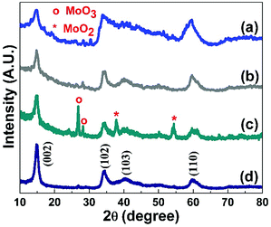
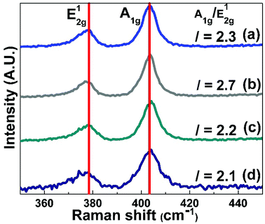
The XRD patterns of synthesised MoS2 and nitrogen-doped MoS2 nanostructures are depicted in Fig. 1(a–d) for 2θ range from 10° to 80°. The intense and broad reflection peaks confirm the formation of the 2H-MoS2 nanostructure for all the prepared compositions. The XRD pattern of the synthesised MoS2 matches the standard MoS2 pattern (JCPDS ICDD no. 37-1492). The observed XRD peaks at 2θ = 14.53°, 32.67°, 33.50°, 35.87°, 39.53°, 58.33°, and 60.14° correspond to (002), (100), (101), (102), (103), (110), and (008) hkl planes of hexagonal MoS2. The XRD patterns of nitrogen-doped MoS2 nanostructures (MoS2-N1 and MoS2-N5) are compared with the XRD patterns of as-synthesised MoS2 and MoS2-400, as depicted in Fig. 1(a–d). After nitrogen doping, there is slight change in the XRD peak intensity, but the peak positions remain the same. In the case of MoS2-N1 sample, the formation of MoO2 and MoO3 along with MoS2 is observed; this clearly indicates the formation of MoO2/MoO3/MoS2 nanocomposites. The reflection peaks due to MoO2 and MoO3 match with JCPDS no. 32-0671 and 47-1081, respectively. Composite formation is observed for MoS2-N1 sample only. Even though the synthesis methods for MoS2-N1 and MoS2-N5 are similar, the conversion of MoS2 to MoO2/MoO3 is different, as seen in the XRD pattern. In the case of MoS2-N1, the amount of carbon available (in the form of urea) to react with oxygen to form carbon dioxide is low as compared to that for MoS2-N5. Therefore, for MoS2-N1, the remaining oxygen reacts with MoS2 to form molybdenum oxide. Thus, we observe difference in oxide formations for MoS2-N1 and MoS2-N5.The broadening of the XRD peak decreases, indicating a more crystalline structure for nitrogen-doped MoS2. The broad XRD peaks confirm that the prepared structures are still in the nanoscale even after heating at 400 °C for nitrogen doping. Furthermore, structural analysis of prepared MoS2 and nitrogen-doped MoS2 are conducted by Raman spectroscopy. Fig. 2(a–d) shows the Raman scattering curves for MoS2, MoS2-400, MoS2-N1 and MoS2-N5 in the range from 350 to 450 cm−1. The two peaks correspond to in-plane (E12g) and out-of-plane (A1g) vibrations at 378 and 403 cm−1 for the synthesised MoS2 materials. These two characteristic Raman peaks confirm the formation of nanoscale MoS2. There is negligible change in the peak separation between A1g and E12g for nitrogen-doped MoS2 compare to that for pristine MoS2. The A1g/E12g ratios for MoS2, MoS2 400, MoS2-N1 and MoS2-N5 are 2.3, 2.7, 2.2 and 2.1, respectively. The A1g/E12g ratio decreases from MoS2 400 to MoS2-N5, confirming that the defect edge sites of MoS2 are occupied by nitrogen species.
The surface and morphological studies of prepared MoS2 nanomaterials were carried out using FESEM and TEM analysis. The magnified images of MoS2, MoS2-400, MoS2-N1, and MoS2-N5 are shown in Fig. 3(a–d). The formation of flower-like nanostructures is observed in the prepared MoS2 samples. The flower-like nanostructure is formed by stacking of nanosheets up to 20–50 nm thickness. As exhibited in Fig. 3(b), MoS2-400 shows growth and an opening of nanosheets into flower-shaped nanostructures. The nitrogen doping in MoS2 nanostructures results in rupturing of nanosheets in MoS2-N1 and MoS2-N5, as shown in Fig. 3(c and d). In the case of MoS2-N1 sample, the existence of rods and rectangular plates is observed, which may be due to the formation of MoO2 and MoO3 nanostructures (ESI, Fig. S1†). Further detailed study related to oxide formation is confirmed by TEM analysis.
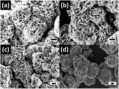 | ||
| Fig. 3 FESEM images of low and high magnification for MoS2 (a), MoS2-400 (b), MoS2-N1 (c), and MoS2-N5 (d). Scale bars 400 nm (black). | ||
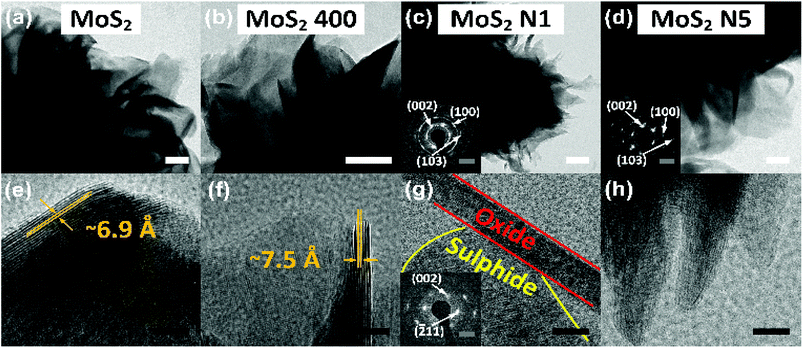
Microstructural analysis of prepared MoS2 nanomaterials was conducted using TEM analysis, and the images are shown in Fig. 4. Fig. 4 shows the TEM images of MoS2 (a and e), MoS2-400 (b and f), MoS2-N1 (c and g) and MoS2-N5 (d and h). The layered structure of prepared MoS2 is confirmed from TEM analysis. TEM clearly indicates the formation of flower-like morphology consisting of stacked nanosheets as flower petals, and this is consistent with the FESEM results. The size of petals in the as-synthesised MoS2 is between 20 and 50 nm; for MoS2-400, the size is between 20 and 80 nm. However, it is observed that the petal size range is decreased to 20–40 nm in the case of MoS2-N1. Every petal is formed by stacking of two-dimensional MoS2 nanosheets, as can be seen in Fig. 4(e–h). As discussed in the FESEM analysis, an opening of the nanosheets in MoS2-400 can be seen in Fig. 4(f) as the interlayer distance increases from ∼6.9 Å to ∼7.5 Å compared with that observed for pristine MoS2. As discussed in XRD and FESEM analysis, the formation of MoO2/MoO3/MoS2 nanocomposites can be seen in Fig. 4(g) for the MoS2-N1 nanomaterial. In the case of MoS2-N5, such composite formation is not observed. The selected area electron diffraction (SAED) pattern confirms that the rod- and plate-like structure shows the oxide phase, whereas the layered flowers exhibit the sulphide phase of nanomaterials. The insets in Fig. 4(c and g) show the SAED patterns for flowers and rods of MoS2-N1 nanomaterials, respectively, whereas the inset in Fig. 4(d) shows the SAED pattern for the flowers of MoS2-N5. The SAED pattern demonstrates intense patterns for different crystallographic planes. The hkl planes (002), (100), and (103) show the sulphide phase for the SAED patterns of MoS2-N1 and MoS2-N5 and are marked in the insets of Fig. 4(c and d). The (002) and (![[2 with combining macron]](https://www.rsc.org/images/entities/char_0032_0304.gif) 11) hkl planes of the oxide phase of MoS2-N1 are shown in Fig. 4(g). The hkl planes and their d spacing exactly match with those calculated from the XRD pattern. To confirm the formation of oxide/sulphide nanocomposites, elemental mapping is carried out, and the results are shown in the ESI (Fig. S2†). The elemental mapping clearly indicates the presence of oxide along with sulphides. Overall, the TEM analysis shows that the results are consistent with the XRD and FESEM results.
11) hkl planes of the oxide phase of MoS2-N1 are shown in Fig. 4(g). The hkl planes and their d spacing exactly match with those calculated from the XRD pattern. To confirm the formation of oxide/sulphide nanocomposites, elemental mapping is carried out, and the results are shown in the ESI (Fig. S2†). The elemental mapping clearly indicates the presence of oxide along with sulphides. Overall, the TEM analysis shows that the results are consistent with the XRD and FESEM results.
X-ray photoelectron spectroscopy (XPS) of the prepared MoS2 samples was conducted to check the elemental composition of the materials. Fig. 5 shows the XPS spectra for MoS2 (a), MoS2-400 (b), MoS2-N1 (c) and MoS2-N5 (d) for binding energies ranging from 394 eV to 408 eV. The N 1s peak around 399.1 eV confirms that nitrogen is present in MoS2-N1 and MoS2-N5 nanomaterials. Mo 3p3/2 can be observed at 395.5 eV in all synthesised materials. The XPS spectra for the Mo 3d peak and S 2p peak and survey scans of the prepared MoS2 nanomaterials are provided in the ESI (Fig. S3†). The sulphur (S) to molybdenum (Mo) atomic percentage ratios for MoS2-N1 and MoS2-N5 are found to be 1.16 and 1.35, respectively. The deviation from the ideal stoichiometric ratio (S![[thin space (1/6-em)]](https://www.rsc.org/images/entities/char_2009.gif) :
:![[thin space (1/6-em)]](https://www.rsc.org/images/entities/char_2009.gif) Mo) indicates the amounts of oxygen and nitrogen present in MoS2-N1 and MoS2-N5 nanomaterials. The nitrogen-to-sulphur atomic percentage ratios are found to be 1.83 and 2.19 for MoS2-N1 and MoS2-N5, respectively. The ratio confirms that the amount of nitrogen present in the MoS2-N5 nanomaterial is higher than that in MoS2-N1 nanostructures.
Mo) indicates the amounts of oxygen and nitrogen present in MoS2-N1 and MoS2-N5 nanomaterials. The nitrogen-to-sulphur atomic percentage ratios are found to be 1.83 and 2.19 for MoS2-N1 and MoS2-N5, respectively. The ratio confirms that the amount of nitrogen present in the MoS2-N5 nanomaterial is higher than that in MoS2-N1 nanostructures.
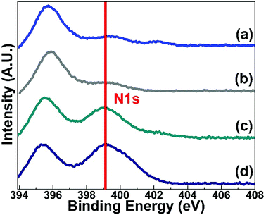 | ||
| Fig. 5 XPS spectra for MoS2 (a), MoS2-400 (b), MoS2-N1 (c) and MoS2-N5 (d) for binding energies ranging from 392 eV to 409 eV. | ||
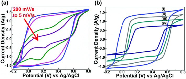
The electrochemical performances of prepared MoS2 nanostructures are studied by cyclic voltammetry (CV) and galvanostatic charge–discharge (GCD) curves using a three-electrode system. The CV curves of the prepared MoS2 nanomaterials were recorded in 1 M H2SO4 electrolyte for scan rates of 5, 20, 100, and 200 mV s−1. The nearly rectangular and symmetric shape of the CV curves can be seen in Fig. 6(a) for as-synthesised MoS2. In Fig. 6(a), the oxidation and reduction peaks for Mo metal centre can be seen at lower step sizes (5 mV s−1 and 20 mV s−1). These peaks lead to pseudocapacitance in the MoS2 materials. The non-regular rectangular CV curve shows electrochemical double layer capacitance in the synthesised MoS2 material. Fig. 6(b) shows a comparison of the CV curves at 200 mV s−1 for MoS2, MoS2-400, MoS2-N1, and MoS2-N5. Furthermore, the capacitive performances of prepared MoS2 nanostructures are evaluated by galvanostatic charge–discharge curves measured at different current densities (2, 3, 4, and 5 A g−1) in 1 M H2SO4 electrolyte. The specific capacitance (Cs) values of the prepared MoS2 nanomaterials are calculated from the GCD curves using the following equation:
| Cs = (I × Δt)/(m × ΔV) |
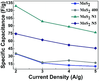 | ||
| Fig. 7 The comparison between specific capacitances (F g−1) of MoS2, MoS2-400, MoS2-N1, and MoS2-N5 vs. specific current (A g−1). | ||
The electrochemical results show the enhanced specific capacitance for MoS2-N1 and MoS2-N5 as compared with that for MoS2. This confirms that nitrogen doping increases the capacitance of MoS2 material. MoS2-N1 shows almost 3.5 times improvement in capacitance value relative to MoS2. MoS2-N1 has higher capacitance than MoS2-N5 due to the presence of N-doped MoO2/MoO3/MoS2 composite material. The main reason behind the increase in specific capacitance can be correlated with the structure of the prepared nanomaterials, the composition and their electronic conductivities.
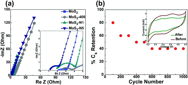
Furthermore, electrochemical impedance spectroscopy (EIS) is performed to understand the charge kinetics and supercapacitor behaviour of prepared MoS2 nanomaterials. Fig. 8(a) shows the Nyquist plots of MoS2, MoS2-400, MoS2-N1 and MoS2-N5. The prepared MoS2 nanostructures show the supercapacitor feature, i.e., a semicircle at higher frequencies and a straight line at the lower frequency region. The intercept on the real axis is ascribed to the equivalent series resistance (Rs), and the diameter of the semicircle corresponds to the charge transfer resistance (Rct) in the electrode/electrolyte system. The Rs values for MoS2, MoS2-400, MoS2-N1 and MoS2-N5 are 2.16, 2.63, 1.89 and 1.16 Ω, respectively. Nitrogen doping decreases the Rs values for MoS2-N1 and MoS2-N5. This confirms that nitrogen doping has enhanced the electrical conductivity of MoS2. The oxide/sulphide composite in MoS2-N1 may be responsible for the higher Rct value (2.2 Ω) in the Nyquist plot compared to that for other MoS2 nanomaterials (<1.5 Ω). The low frequency straight line parallel to the imaginary axis shows the capacitive behaviour of MoS2 nanomaterials (Fig. 8(a)). The highest slope of the straight line is obtained for MoS2-N1, suggesting that MoS2-N1 has optimal performance among the prepared MoS2 nanostructures. The EIS measurements also support that nitrogen doping enhances the conductive performance of prepared MoS2 nanostructures.
The cycling stability of MoS2-N1 material is studied by cyclic charge–discharge at 1 A g−1 current density in 1 M H2SO4 electrolyte. Fig. 8(b) shows the stability of the prepared MoS2-N1 electrode over 1000 cycles. The CV measurements at 100 mV s−1 scan rate are also recorded before and after 1000 cycles. The CV analysis shows almost 70% capacitance retention after 1000 cycles. The charge–discharge cycles show 40% retention in specific capacitance for MoS2-N1 after 1000 cycles.
The synthesised MOS2-N1 shows similar crystallographic phase and structure to that of reported MoS2 nanostructures. The comparison of specific capacitances of prepared MoS2-N1 and reported MoS2 nanostructures at a specific current and electrolyte is depicted in Table 1. In comparison with the reported MoS2 nanostructures, the synthesised MOS2-N1 shows higher specific capacitance at a higher current density, i.e., 129 F g−1 at 2 A g−1 in 1 M of H2SO4. Fig. 7 confirms that the specific capacitance decreases as the specific current increases. Thus, higher specific capacitance at high current density shows the superiority of MoS2-N1 over other reported materials. Therefore, MoS2-N1 is a better electrode material because it exhibits higher specific capacitance at higher specific currents compared to reported 2H-MoS2 materials.
| Sr. no. | Method | Phase | Morphology | Specific capacitance (F g−1) | Reference |
|---|---|---|---|---|---|
| 1 | Hydrothermal | 2-H | Flowers | 129 at 2 A g−1 in 1 M H2SO4 | This work |
| 2 | Two step hydrothermal | 2-H | 3D flower | 168 at 1 A g−1 in 1 M KCl | 34 |
| 3 | DC magnetron sputtering | 2-H | Nanoworms | 138 F g−1 at 1 A g−1 in 1 M Na2SO4 | 35 |
| 4 | Hydrothermal | 2-H | Flower-like | 129.2 F g−1 at 1 A g−1 in 1 M Na2SO4 | 36 |
| 5 | CVD | 2-H | Nanowall | 100 F g−1 at 1 mV s−1 in 0.5 M H2SO4 | 37 |
| 6 | Hydrothermal | 2-H | Nanosphere | 122 at 0.5 A g−1 in 1 M Na2SO4 | 18 |
Conclusion
The successful synthesis of nitrogen-doped MoS2 hierarchical nanostructures was demonstrated by a simple low-cost synthesis method. The structural and morphological characterisation confirmed the formation of flower-like nanostructures of hexagonal MoS2 along with the formation of oxide/sulphide nanocomposites. MoS2-N1 showed specific capacitance of 129 F g−1 at a specific current of 2 A g−1. The formed nitrogen-doped MoO2/MoO3/MoS2 nanocomposites showed four-fold enhancement in specific capacitance than the as-synthesised MoS2 nanostructures. These results suggest that nitrogen-doped MoO2/MoO3/MoS2 nanocomposites can be promising electrode materials for supercapacitor applications.Conflicts of interest
There are no conflicts to declare.Acknowledgements
CK would like to acknowledge to the Director of Indian Institute of Science Education and Research, Pune (IISER Pune) for giving the permission to work at Centre for Materials for Electronics Technology, Pune Lab (C-MET Pune). CK would like to thank the BBK group for providing research facilities and platform. CK would like to acknowledge Dr G. Gund group for valuable guidance and help.Notes and references
- C. Liu, Z. Yu, D. Neff, A. Zhamu and B. Z. Jang, Nano Lett., 2010, 10(12), 4863 CrossRef CAS PubMed.
- J. Zhou, Y. Huang, X. Cao, B. Ouyang, W. Sun, C. Tan, Y. Zhang, Q. Ma, S. Liang, Q. Yan and H. Zhang, Nanoscale, 2015, 7(16), 7035 RSC.
- M. Camara, H. Gualous, F. Gustin and A. Berthon, IEEE Trans. Veh. Technol., 2008, 57(5), 2721 Search PubMed.
- P. Thounthong, S. Rael and B. Davat, J. Power Sources, 2009, 193(1), 376 CrossRef CAS.
- H. Pan, J. Li and Y. Feng, Nanoscale Res. Lett., 2010, 5(3), 654 CrossRef CAS PubMed.
- L. Zhang and X. Zhao, Chem. Soc. Rev., 2009, 38(9), 2520 RSC.
- Y. Tan and J. Lee, J. Mater. Chem. A, 2013, 1(47), 14814 RSC.
- R. Ramachandran, M. Saranya, P. Kollu, B. Raghupathy, S. Jeong and A. Grace, Electrochim. Acta, 2015, 178–647 Search PubMed.
- X. Xie, K. Huang and X. Wu, J. Mater. Chem. A, 2018, 6, 6754 RSC.
- A. Ramadoss, T. Kim, G. Kim and S. Kim, New J. Chem., 2014, 38(6), 2379 RSC.
- M. Javed, C. Zhang, L. Chen, Y. Xi and C. Hu, J. Mater. Chem. A, 2016, 4(22), 8851 RSC.
- L. Cao, S. Yang, W. Gao, Z. Liu, Y. Gong, L. Ma, G. Shi, S. Lei, Y. Zhang, S. Zhang and R. Vajtai, Small, 2013, 9(17), 2905 CrossRef CAS PubMed.
- N. Choudhary, C. Li, H. Chung, J. Moore, J. Thomas and Y. Jung, ACS Nano, 2016, 10(12), 10726 CrossRef CAS PubMed.
- J. Yang, X. Duan, Q. Qin and W. Zheng, J. Mater. Chem. A, 2013, 1(27), 7880 RSC.
- H. Chauhan, M. Singh, S. Hashmi and S. Deka, RSC Adv., 2015, 5(22), 17228 RSC.
- W. Zhang and K. Huang, Inorg. Chem. Front., 2017, 4, 1602 RSC.
- Z. Zhaia, K. Huanga and X. Wub, Nano Energy, 2018, 47, 89 CrossRef.
- M. Acerce, D. Voiry and M. Chhowalla, Nat. Nanotechnol., 2015, 10(4), 313 CrossRef CAS PubMed.
- K. Krishnamoorthy, G. Veerasubramani, S. Radhakrishnan and S. Kim, Mater. Res. Bull., 2014, 50, 499 CrossRef CAS.
- P. Ilanchezhiyan, G. Kumar and T. Kang, J. Alloys Compd., 2015, 634, 104 CrossRef CAS.
- K. Huang, L. Wang, Y. Liu, Y. Liu, H. Wang, T. Gan and L. Wang, Int. J. Hydrogen Energy, 2013, 38, 14027 CrossRef CAS.
- B. Xie, Y. Chen, M. Yu, T. Sun, L. Lu, T. Xie, Y. Zhang and Y. Wu, Carbon, 2016, 99, 35 CrossRef CAS.
- X. Yu, H. Hu, Y. Wang, H. Chen and X. Lou, Angew. Chem., 2015, 54(25), 7395 CrossRef CAS PubMed.
- K. Chang, D. Geng, X. Li, J. Yang, Y. Tang, M. Cai, R. Li and X. Sun, Adv. Energy Mater., 2013, 3(7), 839 CrossRef CAS.
- X. Chen, K. Zhang, Z. An, L. Wang, Y. Wang, S. Sun, T. Guo, D. Zhang and Z. Xue, et al., Int. J. Hydrogen Energy, 2018, 43, 7326 CrossRef CAS.
- J. Li, Y. Hou, X. Gao, D. Guan, Y. Xie, J. Chen and C. Yuan, Nano Energy, 2015, 16, 10 CrossRef CAS.
- J. Deng, H. Li, J. Xiao, Y. Tu, D. Deng, H. Yang, H. Tian, J. Li, P. Ren and X. Bao, Energy Environ. Sci., 2015, 8(5), 1594 RSC.
- J. Zabinski, M. Donley, S. Walck, T. Schneider and N. McDevitt, Tribol. Trans., 1995, 38(4), 894 CrossRef CAS.
- H. Jeong, J. Lee, W. Shin, Y. Choi, H. Shin, J. Kang and J. Choi, Nano Lett., 2011, 11(6), 2472 CrossRef CAS PubMed.
- H. Wang, T. Maiyalagan and X. Wang, ACS Catal., 2012, 2(5), 781 CrossRef CAS.
- P. Chen, J. Yang, S. Li, Z. Wang, T. Xiao, Y. Qian and S. Yu, Nano Energy, 2013, 2(2), 249 CrossRef CAS.
- G. Wang, X. Hu, L. Liu, Y. Yu, H. Lv and A. Chen, J. Mater. Sci.: Mater. Electron., 2018, 29, 5363 CrossRef CAS.
- S. Daia, Z. Liuc, B. Zhaob, J. Zengc and H. Hub, et al., J. Power Sources, 2018, 387, 43 CrossRef.
- X. Wang, J. Ding, S. Yao, X. Wu, Q. Feng, Z. Wang and B. Geng, J. Mater. Chem. A, 2014, 2(38), 15958 RSC.
- A. Sanger, V. K. Malik and R. Chandra, Int. J. Hydrogen Energy, 2018, 43(24), 11141–11149 CrossRef.
- K. Huang, J. Zhang, G. Shi and Y. Liu, Electrochim. Acta, 2014, 132, 397 CrossRef CAS.
- J. M. Soon and K. P. Loh, Electrochem. Solid State Lett., 2007, 10(11), A250–A254 CrossRef CAS.
Footnote |
| † Electronic supplementary information (ESI) available. See DOI: 10.1039/c8ra06660d |
| This journal is © The Royal Society of Chemistry 2018 |

