
 Open Access Article
 This Open Access Article is licensed under a Creative Commons Attribution-Non Commercial 3.0 Unported Licence
Strain-engineering the electronic properties and anisotropy of GeSe2 monolayers†
Zongbao Lia,
Xia Wanga,
Wei Shia,
Xiaobo Xingb,
Ding-Jiang Xue *c and
Jin-Song Huc
*c and
Jin-Song Huc
aSchool of Material and Chemical Engineering, Tongren University, Tongren 554300, China
bCentre for Optical and Electromagnetic Research, South China Academy of Advanced Optoelectronics, South China Normal University, 510006 Guangzhou, China
cCAS Key Laboratory of Molecular Nanostructure and Nanotechnology, Beijing National Research Center for Molecular Sciences, CAS Research/Education Center for Excellence in Molecule Science, Institute of Chemistry, Chinese Academy of Sciences, Beijing 100190, China. E-mail: djxue@iccas.ac.cn
First published on 28th September 2018
Abstract
As a new two-dimensional (2D) material, GeSe2 has attracted significant attention recently due to its distinctive in-plane anisotropic properties originated from the in-plane anisotropic crystal structure, high air stability and excellent performance in polarization-sensitive photodetection. However, no systematic study of the strain effect on the electronic properties and anisotropy of GeSe2 has been reported, restricting the relevant applications such as mechanical-electronic devices. Here we investigate the change of the electronic properties and anisotropy of GeSe2 monolayer under strains along x and y directions through first-principle calculations. The electronic band structure and effective mass of charge carriers are highly sensitive to the strain. Notably, through appropriate x or y directional strain, the anisotropy of the hole effective mass can even be rotated by 90°. These plentiful strain-engineering properties of GeSe2 give it many opportunities in novel mechanical-electronic applications.
1. Introduction
Strain has served as an effective and convenient tool for modulating electronic, transport, and optical properties of semiconductors.1–5 Such strain effects can be interpreted as an elastic field applied to materials, which modifies the geometrical structure of the crystal due to the interaction between the elastic field and crystalline field, then influences the electronic band structure,6 and finally tunes the physical7,8 (such as the optical absorption anisotropy) and chemical properties9 (catalytic properties) of materials. This tool is particularly suitable for the engineering of two-dimensional (2D) crystals because this low-dimensional structure can sustain much larger strain compared with bulk crystals.10–13 For example, monolayer black phosphorus (BP), the most recently studied 2D material, has been reported to be strained up to a remarkable strain of 30% without any dislocation or plastic deformation in its crystal structure,14 providing a wide range for tuning its mechanical and electronic properties.15,16 Furthermore, as the prototypical 2D material with in-plane anisotropy, the anisotropic electrical and thermal properties of ultrathin BP can also be modified by strain.17 It is predicted that the preferred conducting direction of BP can be rotated by 90° in plane through the appropriate biaxial or uniaxial strain (4–6%), providing great opportunities for novel mechanical-electronic device applications.9,10,18,19 Those studies forcefully demonstrated the important function of strain as a powerful tool to modulate the physical properties of materials.20Germanium diselenide (GeSe2), another new important member of in-plane anisotropic 2D materials, has attracted significant attention recently due to its high performance in polarization-sensitive photodetection as well as its great stability in ambient environment.21–27 It adopts a monoclinic crystal structure with the P21/c space group.28 As shown in Fig. 1a and b, the basic building blocks of GeSe4 tetrahedra are mutually connected via corner-sharing forming (GeSe4)n chains along x-axis and via edge-sharing Ge2Se8 double tetrahedral along y-axis. Therefore, the different connection modes lead to in-plane structural anisotropy, which induces strong in-plane anisotropic behaviors of electronic and optical properties. In particular, as a powerful complement to the conventional members of this family with narrow bandgaps such as BP (0.3 eV (ref. 14)), ReS2 (1.5 eV (ref. 28)) and GeSe (1.14 eV (ref. 29 and 30)), GeSe2 has a wide direct bandgap of 2.74 eV,21 making it ideal for the short-wavelength polarized photodetection. In this regard, it will be exciting if we can further modulate the physical properties and anisotropy of GeSe2, thus enabling versatile functionality in this material. Until now, however, there has been no report engineering the physical and corresponding anisotropic properties of GeSe2, and the most recent work only focused on the investigation of the basic in-plane anisotropic properties such as structural, electrical, optical and vibrational anisotropies.
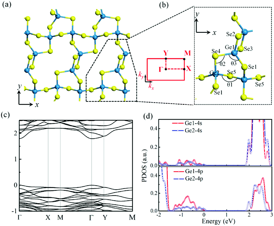 | ||
| Fig. 1 Snapshots of 2D GeSe2 monolayer (a) and the building blocks (b). (c) DFT-calculated band structure of GeSe2 monolayer. The Fermi level is set to zero on the energy axis. (d) Calculated PDOSs of Ge1 and Ge2 atoms labeled in (b). | ||
In this study, through first-principles calculations, we investigate the change of the electronic properties and anisotropy of GeSe2 monolayer under strains along x and y directions. The mechanism for the gap transition is discussed in detail. Furthermore, the strain effects on the effective masses of electrons and holes are systematically investigated. The results of this study indicate that GeSe2, as a new member of anisotropic 2D materials, has promising practical applications in novel mechanical-electronic devices.
2. Computational methods
Based on density functional theory, the geometric and electronic structures of GeSe2 are performed using the Vienna ab initio simulation package (VASP).31,32 Generalized gradient approximation (GGA) with Perdew–Burke–Ernzerhof (PBE) simulates the exchange–correlation energy.33,34 The interactions between valence electrons and ions are described by projector-augmented wave (PAW) potentials.35 Reciprocal space of 6 × 6 × 1 grid is adopted for geometry relaxations and the plane wave basis cutoff energy is set as 600 eV. A sufficiently large vacuum region of 20 Å is applied to avoid the interaction between layers. The convergence criterion is set to be 10−5 eV and the residual force acting on each atom is 10−2 eV Å−1. Since the DFT method is known to underestimate the band gap of semiconductors, it is important to test the robustness of strain effects on the properties of GeSe2. For comparison, we have calculated the band structures of GeSe2 monolayer by DFT and advanced hybrid functional HSE06 methods under different values of axial strains.33 Therefore, the DFT method is employed in this paper to predict the general trends of strain engineering on the band structure of GeSe2 monolayer.For the relaxed GeSe2 monolayer, the applied strain is defined as  , where ai and ai0 are the lattice constants along i (=x and y) direction. The positive values refer to tension while negative values refer to compression. With each applied axial strain, the lattice constant in the transverse direction is fully relaxed for the minimum force. Meanwhile, effective masses of charge carriers are calculated according to the formula
 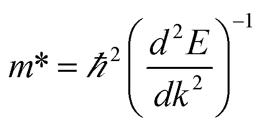 through the calculated band structures, where ℏ is the reduced Planck's constant, E is the energy, and k is the momentum.
3. Results and discussions
We start from the calculation of electronic band structure of GeSe2 monolayer as presented in Fig. 1a. As shown in Fig. 1c, a direct band gap appears at Γ point. It is noteworthy to mention that GeSe2 has highly anisotropic band dispersion along Γ–X and Γ–Y directions of conduct band minimum (CBM) and valence band maximum (VBM), resulting in significantly anisotropic electronic properties. As shown in Fig. 1d and S1,† we further calculate the partial densities of state (PDOS) of unequal Ge atoms and their near-neighbor Se atoms. The results reveal that shallow valence band (SVB, ranging from −1.5 to 0 eV) mainly originate from 4p states of Ge atoms, while Ge1-4p state provides larger contribution than Ge2-4p state. Yet, for the conduction band, Ge-4s states provide larger contribution than Ge-4p states. As shown in Fig. S1a and b,† the VBM is formed mainly by the 4p states of Se atoms in GeSe4 tetrahedra (from Se1 to Se4), while Se5-4p state contributes to SVB. Combining with the large overlap of Ge1-4p and Se-4s states (see in Fig. S1c and d†), the higher contributions to SVB indicates the stronger covalent bond energies of Ge1–Se compared to that of Ge2–Se, resulting in the in-plane anisotropic natural structure of GeSe2 monolayer as shown in Fig. 1a. Therefore, different Ge–Se bonds along x and y directions lead to low in-plane lattice symmetry of GeSe2.We now focus on the band gap modulating of GeSe2 monolayer at different values of axial strains. The components of strain along x and y directions are labeled as εx and εy, respectively. As shown in Fig. 2, it is clear that the HSE06 has a better prediction on the band value of 2.62 eV for GeSe2 monolayer, which is good agreement with our former experimental value of 2.74 eV,20 and has a 0.828 eV energy difference to DFT value. Meanwhile, comparing the calculated band gap values based on HSE06 and DFT methods, one can conclude that the band structures strongly depend on the strains while the both methods give the same band gap variation results as a function of strain. Therefore, the DFT can be employed to predict the general trends of strain engineering on the band structure of GeSe2 monolayer. For the strain εy in Fig. 2a, the maximal band gap of 2.83 eV for HSE06 is obtained at strain εy = −4% and then dropped linearly to 2.01 eV at strain εy = −12%. On the side of tensile strain, the gap shows linear reduction with strain increasing and reaches to 1.51 eV of εy = 12%. To see if the gap could reduce to zero with further increased tensile strain, we explore even larger strain up to +32%. The gap is not found to close while it reaches a minimal value 0.98 eV at +28% strain and then opens up again for larger strain value. Notably, the tensile strain εy presents a strategy for the direct band gap modification with a wide range exceed 1.85 eV. With regard to the strain εx shown in Fig. 2b, the band gap drops to 1.63 eV at compressive strain εx = −12% without sudden change. For the tensile cases, it initially increases from 2.62 eV for the relaxed structure (RS) to a maximal value of 2.83 eV at εx = +8%, and then drops rapidly with further increased expansion. Through the above analysis of strains applied in the two directions, it is obvious that three strain zones are identified for strain εy and two for εx, and the direct band gap is particularly maintained under the in-plane tensile strain along two directions. Briefly, it confirms that the strains can effectively tune the band gap of GeSe2 monolayer in a wide range.
 | ||
| Fig. 2 Band gap of GeSe2 monolayer as a function of strain εy (a) and εx (b) based on the methods of HSE06 and PBE, respectively. Direct/indirect band zones are listed with green/blue color. | ||
To further investigate the specific effect of strain on the band gap turning, the band structures of GeSe2 monolayer under strain in two directions are calculated based on the fully relaxed in-plane anisotropic natural structures. For simplification, we only plot the band structure along remarkable Γ–X (0.5, 0, 0) and Γ–Y (0, 0.5, 0) directions as shown in Fig. 3 and 4, respectively. The red and blue lines are used to highlight the change of the near-gap states of GeSe2 monolayer. As shown in Fig. 3, with the increase of compressive strain εy, the VBM along Γ–Y direction almost unchanged while a steep slope appears along Γ–X direction with the SVB state shifts to lower energy at X point. For CBM, a parallel downward removal introduced with a flat slope along Γ–X(Y) direction accompanied by the compressive strain increasing. On the other side of the increasing tensile strain, the CBM at Γ point has an obviously downward and at Y point moves synchronously, while that at X point almost immovable. Meanwhile, the VBM is always locates at Γ point in the Fermi level with almost invariable slopes along Γ–X and Γ–Y directions. The changes predict that the effect of compressive/tensile strain εy mainly results in a steep slope of the VBM/CBM along Γ–X direction while invariable change along Γ–Y direction. It thus directly reflects the enhanced electrical/hole transport along Γ–X direction under tensile/compressive strain εy because of the larger CBM/VBM slope value, further implies the enhanced anisotropic electrical/hole conductance in-plane of GeSe2 monolayer. And above all, these results reveal that the larger tensile strain εy introduces larger anisotropic electrical properties of GeSe2 than compressive strain εy.
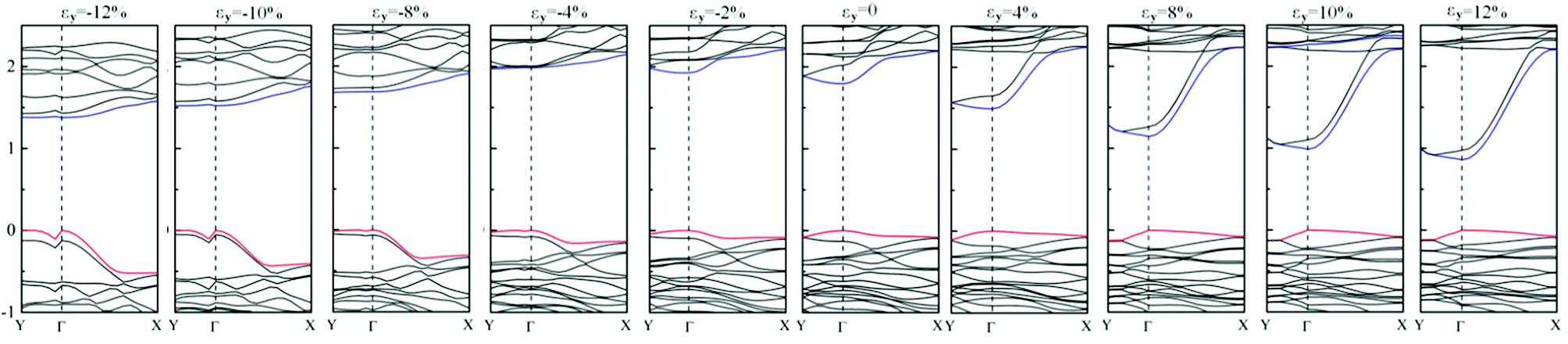 | ||
| Fig. 3 Strain εy manipulated band gap transition in GeSe2 monolayer. The Fermi level is set to 0 eV on the energy axis. The red and blue lines are used to highlight the changing of the energy levels of the VBM and CBM. | ||
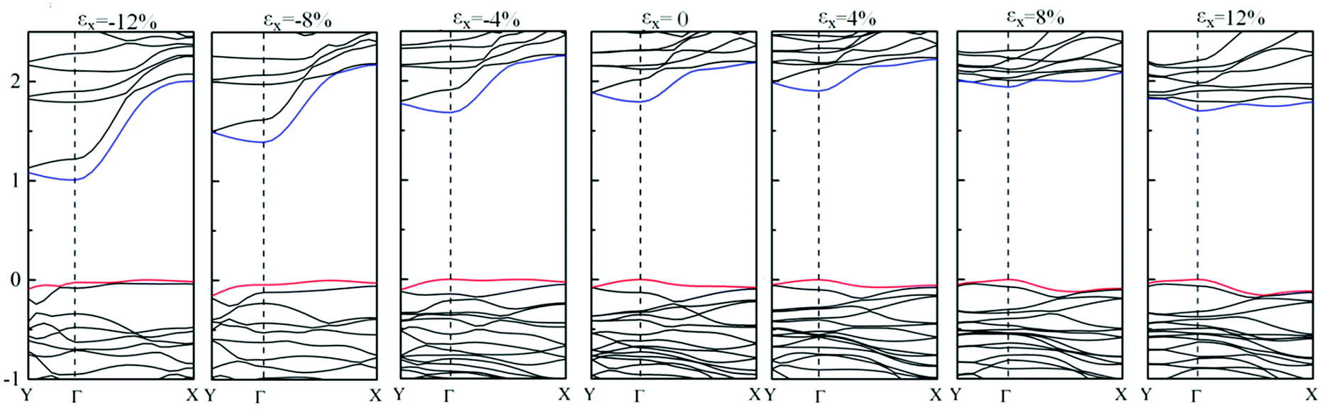 | ||
| Fig. 4 Strain εx manipulated band gap transition in GeSe2 monolayer. The Fermi level is set to 0 eV on the energy axis. All energies are referenced to vacuum level. | ||
Furthermore, it is well known that the direct or indirect nature of the band structure is the result of energy competitions of near-band-edge states under different strains. Fig. 3 exhibits an indirect band in the strain range of −4% to −8%, and then transitions back to direct with larger strain. For example, at εy = −8%, it shows an indirect band gap with the CBM shifts from Γ point to Y with a small energy difference, while the VBM remains at Γ point. Furthermore, the calculated PDOSs for εy = −12% (in Fig. S2†) show that the VBM in the Fermi level mainly originated from Se5/Se1-4p states, SVB is contributed mainly by Se4/Se3-4p states, while Ge-4p states provide large contribution to the VBM. Likewise, at εy = 12% (in Fig. S3†), Se5-4p and Ge2-4s/4p orbitals result mainly in the CBM.
Meanwhile, Fig. 4 shows the effect of strain εx on the band structure of GeSe2 monolayer. In contrast to the effect of strain εy on tuning of CBM/VBM, the change of CBM/VBM on the compressive/tensile strain εx exhibits a reverse tendency that tensile strain affects the VBM while compressive strain CBM. In summary, for the case of the two applied strains, the CBM tuning along Γ–X can be easier obtained by lattice expansion along y direction and introduced anisotropic electrical properties, especially the anisotropy electrical/hole conductance.
To further investigate the changes of the electronic structures under different strains, the crystal parameters (denoted in Fig. 1b) of GeSe2 monolayer are listed in Table 1 for the major strain of εx = 12% and −12%, while the crystal structures are shown in Fig. S4.† As shown in Table 1, the change of parameter b (along y direction) is smaller than that of parameter a under strains, which shows large crystal distort in-plane of GeSe2. For example, with the change of parameter a as 12% (εx = 12%), the change of b is ∼−2.14%, respectively. Under strains, it reveals that the bond lengths substantially retained while angels show marked change. The in-plane unsynchronized lattice change induces corrugated structure along x direction (see Fig. S4†), then enhance the structural anisotropy of GeSe2 monolayer, further introduce the anisotropy of electronic structure (see Fig. 3 and 4). Form the decomposed charge density of the CBM under different strains, it can be seen that the strain εx = −12% introduces a significant enhanced charge distribution along x direction in real space while almost average in two directions under strain εx = 12%, which coincides with the band structure analysis in Fig. 4.
| Strain εx | Lattice parameters (Å) | Bond length (Å) | Angle (°) | |||||||
|---|---|---|---|---|---|---|---|---|---|---|
| a | b | Ge2–Se4 | Ge2–Se1 | Ge1–Se4 | Ge1–Se1 | Ge1–Se2 | θ1 | θ2 | θ3 | |
| 12% | 7.957 | 16.73 | 2.370 | 2.350 | 2.373 | 2.373 | 2.373 | 109.38 | 101.54 | 113.85 |
| 0 | 7.104 | 17.095 | 2.360 | 2.353 | 2.372 | 2.392 | 2.375 | 100.18 | 98.45 | 100.49 |
| −12% | 6.252 | 17.416 | 2.346 | 2.368 | 2.355 | 2.409 | 2.370 | 88.96 | 93.99 | 106.65 |
Because the electrical/hole transport behavior is usually decided by the lowest/highest-energy edge, the obvious edges variety indicate the effective mass change, then approximately implied the alterable mobility along two directions. Fig. 5 demonstrates the evolution of the electron and hole effective masses as a function of both strain εx and εy. It is obvious that a significant enhanced anisotropic electron (hole) appears for the strain larger than εy = −4%. In the strain range from −8% to −4% in Fig. 5a, a sudden jump of electronic effective mass along Γ–Y is due to the completion of CBM at Y and Γ points for the direct–indirect band gap transition. For the larger strain at εy = 12%, the effective mass of electron along Γ–Y direction is an order of magnitude bigger than that along Γ–X direction, indicating that the electron prefers transport in-plane x direction of crystal structure. On the other hand, the small hole effective mass shows the preferred transport direction along y of the direct band structure (Fig. 5b). With the case of strain applied in x direction, a noticeable anisotropy is introduced to the hole effective mass (Fig. 5d), while the electron effective mass shows a small anisotropic variation (Fig. 5c). As shown in Fig. 5d, the opposite change presents the fact that the hole prefers transport along x direction under strain. Therefore, the above discussion reveals that the strain can dramatically increase or decrease the effective masses of carriers in the GeSe2 monolayer with a noticeable anisotropy introduced, and even reverse the anisotropy of hole effective mass.
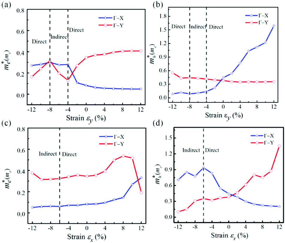 | ||
| Fig. 5 Effective masses of the electron (left) and hole (right) as a function of strain εy (top) and εx (bottom). Three (two) strain zones for εy (εx) are also labelled. me depicts the free electron mass. | ||
4. Conclusions
In summary, we have studied the strain effect on the electronic band structure and anisotropy of GeSe2 monolayer through first-principle calculations. The band gap of GeSe2 monolayer can be effectively tuned by strain in a wide range. The effective mass of electrons and holes are also highly sensitive to the strain. Particularly, the anisotropy of hole effective mass can even be rotated by 90° through applying appropriate x or y direction strain. These intriguing properties demonstrate the great potential of GeSe2 monolayer for novel mechanical-electronic device applications.Conflicts of interest
There are no conflicts to declare.Acknowledgements
This work is supported by the National Natural Science Foundation of China (21573249, 21403078), the Strategic Priority Research Program of the Chinese Academy of Sciences (Grant No. XDB12020100), the Youth Innovation Promotion Association CAS (2017050), Natural Science Foundation of Guizhou Province (20161150, 201567), and Provincial Key Disciplines of Chemical Engineering and Technology in Guizhou Province (No. ZDXK20178).References
- R. S. Jacobsen, K. N. Andersen, P. I. Borel, J. Fage-Pedersen, L. H. Frandsen, O. Hansen, M. Kristensen, A. V. Lavrinenko, G. Moulin, H. Ou, C. Peucheret, B. Zsigri and A. Bjarklev, Nature, 2006, 441, 199–201 CrossRef CAS PubMed.
- V. Tran, R. Soklaski, Y. Liang and L. Yang, Phys. Rev. B: Condens. Matter Mater. Phys., 2014, 89, 235319 CrossRef.
- W. Y. Yu, C. Y. Niu, Z. L. Zhu, X. F. Wang and W. B. Zhang, J. Mater. Chem. C, 2016, 4, 6581–6587 RSC.
- J. K. Jiang, Q. H. Liang, S. L. Zhang, R. S. Meng, C. J. Tan, Q. Yang, X. Sun, H. Y. Ye and X. P. Chen, J. Mater. Chem. C, 2016, 4, 8962–8972 RSC.
- M. J. Zhang, Y. P. An, Y. Q. Sun, D. Peng, X. N. Chen, T. X. Wang, G. L. Xu and K. Wang, Phys. Chem. Chem. Phys., 2017, 19, 17210 RSC.
- D. Çakır, H. Sahin and F. M. Peeters, Phys. Rev. B: Condens. Matter Mater. Phys., 2014, 90, 205421 CrossRef.
- J. Feng, X. Qian, C. W. Huang and J. Li, Nat. Photonics, 2012, 6, 866–872 CrossRef CAS.
- Z. Zhang, L. Li, J. Hong, N. Z. Wang, F. Yang and Y. Yu, Nano Lett., 2017, 17, 6097–6103 CrossRef CAS PubMed.
- H. Li, C. Tsai, A. L. Koh, L. Cai, A. W. Contryman, A. H. Fragapane, J. H. Zhao, H. S. Han, H. C. Manoharan, A. P. frank, J. K. Norskov and X. L. Zheng, Nat. Mater., 2016, 15, 48–53 CrossRef CAS PubMed.
- A. S. Rodin, A. Carvalho and A. H. Castro Neto, Phys. Rev. Lett., 2014, 112, 176801 CrossRef CAS PubMed.
- X. H. Peng, Q. Wei and A. Copple, Phys. Rev. B: Condens. Matter Mater. Phys., 2014, 90, 085402 CrossRef.
- K. S. Kim, Y. Zhao, H. Jang, S. Y. Lee, J. M. Kim, K. S. Kim, J. H. Ahn, P. Kim, J. Y. Choi and B. H. Hong, Nature, 2009, 457, 706–710 CrossRef CAS PubMed.
- C. Lee, X. D. Wei, J. W. Kysar and J. Hone, Science, 2008, 321, 385–388 CrossRef CAS PubMed.
- Q. Wei and X. Peng, Appl. Phys. Lett., 2014, 104, 251915 CrossRef.
- H. F. Lin, L. M. Liu and J. J. Zhao, J. Mater. Chem. C, 2017, 5, 2291–2300 RSC.
- V. Tran, R. Soklaski, Y. Liang and L. Yang, Phys. Rev. B: Condens. Matter Mater. Phys., 2014, 89, 817 Search PubMed.
- R. Fei and L. Yang, Nano Lett., 2014, 14, 2884–2889 CrossRef CAS PubMed.
- H. Liu, A. T. Neal, Z. Zhu, Z. Luo, X. Xu, D. Tomanek and P. D. Ye, ACS Nano, 2014, 8, 4033–4041 CrossRef CAS PubMed.
- J. Qiao, X. Kong, Z.-X. Hu, F. Yang and W. Ji, Nat. Commun., 2014, 5, 4475 CrossRef CAS PubMed.
- Y. L. Mao, C. S. Xu, J. M. Yuan and H. Q. Zhao, Phys. Chem. Chem. Phys., 2018, 20, 6929–6935 RSC.
- Y. S. Yang, S. C. Liu, W. Yang, Z. B. Li, Y. Wang, X. Wang, S. S. Zhang, Y. Zhang, M. S. Long, G. M. Zhang, D. J. Xue, J. S. Hu and L. J. Wan, J. Am. Chem. Soc., 2018, 140, 4150–4156 CrossRef CAS PubMed.
- X. Zhou, X. Hu, S. Zhou, Q. Zhang, H. Li and T. Zhai, Adv. Funct. Mater., 2017, 27, 1770279 CrossRef.
- Y. Q. Wei, L. Huang, J. He, Y. P. Guo, R. H. Qin, H. Q. Li and T. Y. Zhai, Adv. Energy Mater., 2018, 8, 1703635 CrossRef.
- B. Mukherjee, Z. B. Hu, M. R. Zheng, Y. Q. Cai, Y. P. Feng, E. S. Tok and C. H. Spw, J. Mater. Chem., 2012, 22, 24882–24888 RSC.
- X. F. Fang, B. Liu, Q. F. Wang, W. F. Song, X. J. Hou, D. Chen, Y. B. Cheng and G. Z. Shen, Adv. Mater., 2013, 25, 1479–1486 CrossRef PubMed.
- M. Xu, S. Jakobs, R. Mazzarello, J. Y. Cho, Z. Yang, H. Hollermann, D. H. Shang, X. S. Miao, Z. H. Yu, L. Wang and M. Wutting, J. Phys. Chem. C, 2017, 121, 25447–25454 CrossRef CAS.
- Q. Lin, Y. Li, M. Xu, Q. Cheng, H. Qian, J. L. Feng, H. Tong and X. S. Miao, IEEE Electron Device Lett., 2018, 39, 496–499 Search PubMed.
- F. C. Liu, S. J. Zheng, X. X. He, A. Chaturvedi, J. F. , He, W. L. Chow, T. R. Mion, X. L. Wang, J. D. Zhou, Q. D. Fu and H. J. Fan, Adv. Funct. Mater., 2016, 26, 1169–1177 CrossRef CAS.
- X. Wang, Y. Li, L. Huang, X. W. Jiang, L. Jiang, H. Dong, Z. Wei, J. Li and W. Hu, J. Am. Chem. Soc., 2017, 139, 14976–14982 CrossRef CAS PubMed.
- S. C. Liu, Y. Mi, D. J. Xue, Y. X. Chen, C. He, X. F. Liu, J. S. Hu and L. J. Wan, Adv. Electron. Mater., 2017, 3, 1700141 CrossRef.
- G. Kresse and J. Furthmuller, Phys. Rev. B: Condens. Matter Mater. Phys., 1996, 54, 11169 CrossRef CAS.
- G. Kresse and D. Joubert, Phys. Rev. B: Condens. Matter Mater. Phys., 1999, 59, 1758 CrossRef CAS.
- J. White and D. Bird, Phys. Rev. B: Condens. Matter Mater. Phys., 1994, 50, 4954 CrossRef CAS.
- J. P. Perdew, K. Burke and M. Ernzerhof, Phys. Rev. Lett., 1996, 77, 3865 CrossRef CAS PubMed.
- P. E. Blöchl, Phys. Rev. B: Condens. Matter Mater. Phys., 1994, 50, 17953 CrossRef.
Footnote |
| † Electronic supplementary information (ESI) available. See DOI: 10.1039/c8ra06606j |
| This journal is © The Royal Society of Chemistry 2018 |