 Open Access Article
Sn-doped 3D ATO inverse opal/hematite hierarchical structures: facile fabrication and efficient photoelectrochemical performance†
Junjie Zhang,
Jing Li,
Boxue Zhang,
Jianfeng Ye ,
Yun Wang
 * and
Xiaozhou Ye
 *
*
Department of Chemistry, College of Science, Huazhong Agricultural University, Wuhan 430070, China. E-mail: xzye@mail.hzau.edu.cn; yunwang123@126.com
First published on 18th December 2018
Abstract
The coupling of hematite with a three-dimensional (3D) conductive inverse opal (IO) skeleton provides an efficient route to enhance the photoelectrochemical (PEC) properties of hematite without changing its chemical composition. In this work, novel 3D antimony-doped SnO2 (ATO) IO/hematite heterostructures were facilely fabricated, and their PEC properties were thoroughly studied. Analysis of the morphologies and photocurrent densities of the 3D ATO IO//Fe2O3 heterostructures reveals that the high conductivity of the ATO skeleton as well as the high specific area and good light harvesting properties of the 3D IO structures greatly enhance their PEC performance. In particular, further morphology tuning by changing the diameters of the ATO IO skeletons could optimize the optical and electrical properties of the as-prepared heterostructures, demonstrating the important influence of morphology engineering on PEC performance. Moreover, after a simple Sn-doping process, the PEC properties of the as-prepared structure could be further enhanced; a photocurrent density of 1.28 mA cm−2 at 1.23 V vs. RHE was obtained under AM 1.5G illumination.
Introduction
With increasing concerns regarding the greenhouse effect and the global energy crisis, photoelectrochemical (PEC) water splitting has attracted worldwide attention as a promising solution to address these environmental and energy issues.1,2 Since TiO2 was first used as a photoelectrode for PEC water splitting as reported by Fujishima and Honda in 1972,3 numerous other semiconductors have been studied as possible candidates, such as CdS,4 WO3,5 and BiVO4,6 and they have exhibited promising PEC performance. Among these, hematite has attracted particular attention due to its suitable band gap (Eg = 2.2 eV) for efficient light absorption, excellent chemical stability for resistance to photocorrosion, and a high theoretical water splitting efficiency of around 12.4%.7–9 However, the reported PEC properties of hematite-based photoanodes are very different from those of theoretical models; this may be due to several drawbacks presented by intrinsic factors of hematite, such as low absorption coefficients, short hole diffusion lengths (2 to 4 nm), short photo-generated charge carrier lifetimes (<10 ps), and poor electrical conductivity.10,11Many strategies have been developed to solve those problems and enhance the PEC properties of hematite-based anodes. Among these, element doping, such as doping with Ti, Sn, or Si, can improve the electron conductivity of hematite and hence improve the charge transfer of hematite electrodes.12–14 In particular, Sn ions can be readily incorporated into hematite due to their similar ionic radius and Pauling electronegativity to Fe ions.15 It was found that Sn-doping is effective to improve the electronic conductivity of hematite.9,15 Also, Sn incorporation can change the morphology16,17 and surface of hematite,18 resulting in decreased electron–hole recombination and additional enhancement of PEC performance.18–20
In addition to element doping, constructing hematite compositions with nanostructured electron-conductive substrates has received much attention.21 By depositing hematite thin films or nanoparticles on nanostructured substrates of conductive materials, the charge transfer properties of hematite can be greatly improved, and electron–hole recombination loss can be decreased.8 Transparent conducting oxides (TCO), such as F-doped SnO2 (FTO), Sb-doped SnO2 (ATO), and Al-doped ZnO (AZO), have advantages of profound electronic conductivity and high transparency in the visible region of the spectrum; they are perfect candidates for hosting hematite to construct composite photoanodes for water splitting.22,23 In this regard, ITO nanowire arrays,24 FTO nanocone arrays,25,26 ATO nanorod arrays,27 and ATO 3D skeletons28 have been used as nanostructured conductive substrates on which to deposit hematite nanoparticles or thin films, and the resulting heterostructures exhibit greatly enhanced PEC properties compared to pristine hematite.
In addition, the morphologies of the heterostructures can be designed and tuned to increase the interfacial area of hematite and the electrolyte and facilitate light absorption to further enhance the PEC properties.26 The 3D inverse opal (IO) structure is the inverse replica of 3D colloidal crystal.29 Due to its periodically ordered macroporous structures, 3D IOs have photonic effects, where the light absorption in specific wavelength regions can be strongly enhanced by altering the diameter of the IOs.5,30 Hence, 3D IO structures are widely employed to construct photoanodes to improve their light utilization performance.5,31 For example, Liu et al.32 fabricated SrTiO3 3D inverse opals with different pore sizes and investigated their water splitting properties. The overlap of the photonic stop-band with its band gap was achieved by choosing suitable pore sizes for the IO structures. As a result, compared with disordered porous SrTiO3, notably enhanced efficiency of water splitting of 3DOM SrTiO3 was realized due to the slow photon effect.
On the other hand, it has been well-documented that 3D inverse opal structures can also provide favorable charge transport properties4 due to their ordered interconnected macropores.33 In addition, 3D inverse opal structures have relatively large surface areas without accelerating charge recombination.34,35 For example, 3D graphene inverse opal was fabricated on FTO and used as a substrate on which to deposit hematite.36 The photocurrent density of α-Fe2O3/GIO in water splitting is 1.4 times greater than that of hematite. It was confirmed that the improvement was due to decreased electron–hole recombination and the shortened charge transfer distance between hematite and the conducting graphene substrate. There are also several studies on the fabrication of 3D IO ATO and hematite host–guest structures,28,37 which exhibit improved PEC properties. However, for these IO heterostructures, there are few studies discussing their morphology-related light utilizing properties and PEC properties. Herein, we report the fabrication of ATO IO/Fe2O3 composite structures with PEC properties. In this photoanode design, the highly conductive ATO IO acts as an effective conductive skeleton and provides a relatively high surface area for loading of photoactive hematite, which provides fast and direct electrical transport paths. In addition, to further investigate the influence of the morphologies of the heterostructures on their light harvesting and PEC properties, ATO IO/Fe2O3 composite structures with three different diameters were designed and fabricated. As a result, the as-fabricated 3D ATO IO/Fe2O3 composite structures with suitable pore diameters presented enhanced PEC performance, achieving 1.04 mA cm−2 at 1.23 V vs. RHE, which is 8 times that of the reference planar ATO/Fe2O3 sample. Moreover, we further enhanced the photocurrent densities of the samples by Sn-doping, and the enhancement mechanism was also studied.
Experimental
Materials
All chemicals used were of analytical grade. Tin(IV) chloride pentahydrate (SnCl4·5H2O, >99.7%), iron trichloride hexahydrate (FeCl3·6H2O, >99.0%), antimony(III) chloride (SbCl3, >99.0%), sodium nitrate (NaNO3, >99.0%), sodium hydroxide (NaOH, >96.0%), and ethanol (>99.7%) were obtained from Sinopharm Chemical Reagent Co., Ltd. Fluorine-doped tin oxide (FTO) coated glass (<14 Ω sq−1, 2.2 mm thick) was obtained from Wuhan Jinge Solar Energy Technology Co., Ltd.Preparation of ATO IO/Fe2O3 structures and planar ATO/Fe2O3 films
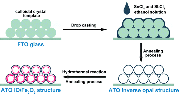
The fabrication process of the ATO IO/Fe2O3 structures is presented in Scheme 1. Firstly, ATO inverse opals (IO) were prepared by modified drop casting methods.5 Typically, polystyrene spheres (PS) with diameters of 220, 330, and 670 nm were assembled on fluorine-doped tin dioxide (FTO) substrates (1 cm × 2.5 cm) using a vertical deposition technique38 to form colloidal crystal thin films. Then, 0.25 mmol SbCl3 and 0.75 mmol SnCl4·5H2O were both dissolved in 5 mL absolute ethanol, yielding a translucent precursor solution. The final concentrations of SbCl3 and SnCl4·5H2O were 0.05 M and 0.15 M, respectively. Then, 10 μL precursor solution was dropped on the colloidal crystal template and subsequently dried in a 100 °C oven. After the film was cooled to room temperature, the same procedure was repeated. The colloidal crystal templates were then removed by high temperature annealing at 500 °C for 2 h under ambient air, and ATO IO films were obtained.Secondly, a Fe2O3 layer was coated on the ATO IO films by a hydrothermal reaction. Typically, 0.8 mmol FeCl3·6H2O and 1.6 mmol NaNO3 were dissolved in 20 mL distilled water to obtain a yellow solution. Then, the solution was transferred into a 25 mL Teflon-lined stainless steel autoclave, and the as-prepared ATO IO films were also placed in the autoclave vertically. The reaction was carried out in a 120 °C oven for 2 h. After the reaction, a thin layer of akaganeite phase (FeOOH) nanoparticles was grown on the ATO IO skeleton.39 The obtained ATO IO(330)/FeOOH films were rinsed with distilled water and ethanol and dried overnight. Finally, the obtained films were annealed in air at 550 °C for 2 h and 750 °C for 30 minutes with a ramping rate of 3 °C min−1, and red thin films of the ATO IO/Fe2O3 composite structure were obtained.40 Using colloidal crystals assembled from PS spheres with diameters of 220, 330, and 670 nm, we prepared ATO IO/Fe2O3 samples with pore sizes of 220, 330, and 670 nm. The samples were denoted as ATO IO(220)/Fe2O3, ATO IO(330)/Fe2O3, and ATO IO(670)/Fe2O3, respectively. To investigate the advantages of the ATO IO/Fe2O3 structures for their PEC properties, a planar control sample was prepared with a similar fabricating process using FTO substrate without colloidal crystal templates. The obtained control sample was designated as planar ATO/Fe2O3.
For Sn-doping, the manufacturing process was the same as for the undoped sample at first. After the fabrication of ATO IO and the following hydrothermal reaction, the ATO IO(330)/FeOOH film was obtained. Then, the film was dipped in 20 mM SnCl4–ethanol solution for 10 minutes to allow Sn4+ to absorb on the surfaces of the FeOOH nanoparticles. Then, the ATO IO(330)/FeOOH samples were annealed in air at 550 °C for 2 h and 750 °C for 30 minutes with a ramping rate of 3 °C min−1, as with the undoped samples. The as-prepared structure was denoted as Sn-doped ATO IO/Fe2O3.
Characterization
The samples were characterized by field-emission scanning electron microscopy (FE-SEM, Hitachi SU8010), transmission electron microscopy (TEM), high-resolution TEM (HRTEM, JEM-200CX) equipped with energy-dispersive X-ray spectroscopy (EDS), powder X-ray diffraction (XRD, Bruker D8, Cu Kα radiation), UV-vis spectroscopy (UV-2450, Shimadzu), and X-ray photoelectron spectroscopy (XPS, Escalab 250Xi).Photoelectrochemical measurements
All photoelectrochemical measurements were performed using an Autolab potentiostat in a three-electrode electrochemical cell with a platinum coil as the counter electrode and Hg/HgO as the reference electrode. The electrolyte was 1 M NaOH (pH 13.6) aqueous solution. The samples were covered with nonconductive epoxy resin to obtain a working area of 0.25 cm2. Linear sweep voltammograms (LSVs) were measured under dark or one-sun conditions (Xe lamp, 100 mW cm−2, AM 1.5G) with a sweep rate of 10 mV s−1. The values of the potentials relative to the reversible hydrogen electrode (RHE) were calculated by the Nernst equation:| VRHE = VHg/HgO + V0Hg/HgO + 0.059pH | (1) |
The electrochemical impedance spectra (EIS) were recorded using a CHI660C workstation (CH Instrument, Inc.) under illumination at an applied potential of 1.23 V vs. RHE in the frequency range from 1 MHz to 0.01 Hz. Mott–Schottky measurements were performed in 1 M NaOH under dark conditions with a frequency of 1 kHz. The incident photon-to-current conversion efficiency (IPCE) was measured with a bias of 1.23 V vs. RHE using a specially designed IPCE system.
Results and discussion
Fig. 1 shows typical SEM images of the as-prepared ATO IO and ATO IO/Fe2O3 structures. Fig. 1a shows the top view of the ATO IO fabricated from periodic colloidal crystal templates using PSs 330 nm in diameter. Because of the shrinkage of the ATO IOs during the fabricating process, the diameters of the macropores of the as-fabricated ATO IO are around 280 nm. There are also pores between neighboring macropores with diameters of about 50 to 60 nm, which improves the infiltration of FeCl3 precursor solution into the IO structure.41 Then, after the hydrothermal reaction in FeCl3 precursor solution at 120 °C and calcination at 550 °C, a layer of Fe2O3 film was evenly grown on the surface of the ATO IO; the well-ordered face-centered cubic arrangement was retained, as shown in Fig. 1b. From Fig. 1c, it can be seen that the Fe2O3 film is composed of Fe2O3 nanorods growing radially from the ATO surface. The thickness of the Fe2O3 film is around 50 to 60 nm, and the pore diameter of the IO structure is about 160 nm. From the cross sectional image (Fig. 1d), it can be seen that the thickness of the Fe2O3/ATO structure is around 8 to 9 μm.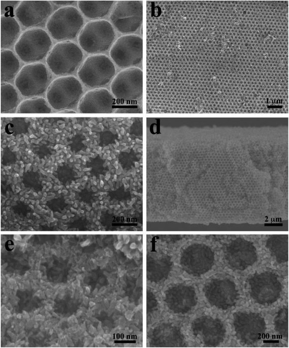 | ||
| Fig. 1 FE-SEM images of (a) 330 nm ATO IO; (b and c) top views and (d) cross section view of ATO IO(330)/Fe2O3, (e) ATO IO(220)/Fe2O3 film and (f) ATO IO(670)/Fe2O3 film. | ||
By using PS spheres with different diameters to assemble the colloidal crystal templates, the pore diameters and, thus, the periodicities of the ATO IO/Fe2O3 structures can be readily adjusted. As shown in Fig. 1e and f, ATO IO(220)/Fe2O3 and ATO IO(670)/Fe2O3 structures could be obtained by using PS spheres with diameters of 220 nm and 670 nm, respectively. The thicknesses of the Fe2O3 films in both structures are around 50 nm, which is the same as that of ATO IO(330)/Fe2O3. This may be because the same fabricating conditions were used for the Fe2O3 films in these three structures. In addition, as the diameters of PS spheres decreased from 670 nm to 220 nm, the pore diameters of the IO structures steadily decreased. Accordingly, the pore diameters of ATO IO(220)/Fe2O3 decreased to less than 100 nm, which may be unfavorable for electrolyte infiltration during PEC tests.
To further confirm the core/shell structure of the ATO IO/Fe2O3 structures, TEM images of the ATO IO(330)/Fe2O3 sample were acquired, as shown in Fig. 2. The low-resolution view (Fig. 2a) confirms that Fe2O3 nanorods are tightly coated on the ATO IO skeleton and form a layer of Fe2O3 film. The thickness of the Fe2O3 film is roughly 55 to 60 nm, in accordance with the SEM images. Fig. 2b shows a high resolution TEM image of the Fe2O3 nanorods, which verifies that the as-prepared Fe2O3 nanorods adopt hematite phase with an interplanar lattice spacing of 0.25 nm from the (110) plane.
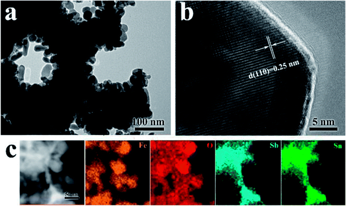 | ||
| Fig. 2 (a and b) HRTEM images and (c) STEM image with element mappings of the ATO IO(330)/Fe2O3 sample. | ||
Furthermore, the compositions and elemental distributions of the ATO IO/Fe2O3 structures were checked by STEM-EDS element mapping, as shown in Fig. 2c. The Sn and Sb elements are homogeneously distributed on the inverse opal skeleton region, which indicates that Sb element was uniformly inserted in the SnO2 lattice and formed ATO. However, Fe element was located around the surface regions of the ATO IOs. This phenomenon confirmed that Fe2O3 was distributed on the surfaces of the ATO IOs.
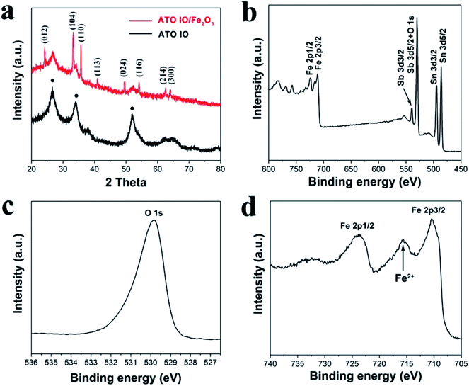
To confirm the crystal structures and crystallinities of the as-prepared ATO IO/Fe2O3 structures, X-ray diffraction (XRD) patterns of the ATO IO and ATO IO(330)/Fe2O3 samples were acquired and are shown in Fig. 3a. For the ATO IO sample, all the diffraction peaks match well with SnO2 cassiterite phase (JCPDS no. 41-1445) without any impurity diffraction peaks, which indicates that Sb acts as a dopant in the SnO2 lattice. The relatively broad peaks of these two samples indicate the presence of small crystallites in the ATO IO structure. For ATO IO(330)/Fe2O3, in addition to the diffraction peaks of ATO, the characteristic diffraction peaks of (012), (104), (110), (113), (024), (116), (214), and (300) can be indexed to pure hematite phase (JCPDS no. 33-0664).
The composition of the ATO IO/Fe2O3 sample was further characterized by X-ray photoelectron spectroscopy (XPS). According to the survey spectra shown in Fig. 3b, Fe 2p, Sb 3d, Sn 3d and O 1s were detected in the sample. The Sb 3d peak may mainly arise due to the incorporation of dopant ions from the ATO inverse opals. The peak at 529.8 eV in the high-resolution spectrum in Fig. 3c was assigned to the O2− ions in Fe2O3. The sample showed two characteristic Fe 2p bands, as shown in Fig. 3d, which were located at ∼724 eV (Fe 2p1/2) and ∼710 eV (Fe 2p3/2), respectively. It is worth noting that there was a Fe(II) band located at ∼716 eV, which suggests that high-valent Sn(IV) ions substituted and/or occupied vacant interstitial sites and reduced Fe3+ to Fe2+ to maintain overall charge neutrality. This indicates that some Sn(IV) ions from ATO IO may have been doped into the Fe2O3 lattice through thermal diffusion.42
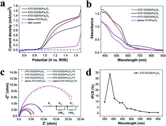
The photoelectrochemical (PEC) properties of the ATO IO/Fe2O3 electrodes with different diameters were studied both in the dark and under simulated AM 1.5G illumination (100 mW cm−2) in 1 M NaOH electrolyte (pH = 13.6). For comparison, a planar ATO/Fe2O3 photoanode was fabricated by a similar process without IO templates. As shown in the resulting linear sweep voltammograms (LSVs) in Fig. 4a, as the applied positive potential increased, the photocurrents increased steadily under illumination, while the dark currents were negligible. It is clear that the ATO IO/Fe2O3 electrodes showed better performance than the planar sample over the potential range from 0.6 to 1.7 V vs. RHE. At 1.23 V vs. RHE, the photocurrent densities of the ATO IO(220)/Fe2O3, ATO IO(330)/Fe2O3, and ATO IO(670)/Fe2O3 photoanodes were 0.88 mA cm−2, 1.04 mA cm−2, and 0.69 mA cm−2, which are 7 times, 8 times and 5 times higher than that of the planar ATO/Fe2O3 electrode (0.13 mA cm−2), respectively. The enhanced PEC performance of the ATO IO/Fe2O3 photoanode compared to the planar control can be attributed to the following reasons. Firstly, the inverse opal structure has periodically arranged macropores that connect very well with each other, which allows efficient charge transport to the conducting substrates and electrolyte. Another benefit is the enhanced light trapping effect due to the multi-pass scattering of incident light originating from the 3D periodical structures, which will be discussed later.
It is worth mentioning that the photocurrent densities of the three inverse opal electrodes with different diameters are different. Firstly, the photocurrent density of ATO IO(220)/Fe2O3 is lower than that of the ATO IO(330)/Fe2O3 photoanode over the tested potential range. This may be due to the smaller pore sizes of the ATO IO(220)/Fe2O3 sample, which leads to smaller and fewer voids inside the IO structure; this may be unfavorable for mass infiltration and transfer inside the photoanode.33 On the other hand, the photocurrent density of ATO IO(670)/Fe2O3 is the lowest among the three ATO IO/Fe2O3 samples, which may be due to its less enhanced light absorption, as discussed later.
To investigate and understand the improved PEC performance of the ATO IO/Fe2O3 structures, UV-vis absorption spectra of the ATO IO/Fe2O3 samples with different diameters as well as the planar ATO/Fe2O3 sample were measured and are shown in Fig. 4b. Firstly, it is unfortunate that the as-prepared ATO IO/Fe2O3 samples did not show specific absorption peaks at the photonic bandgaps, which may be due to the rough Fe2O3 layer inside ATO IO structure and the polycrystalline nature of the IO structure. However, the three ATO IO/Fe2O3 samples still exhibited strong and broad absorption enhancement compared to the planar control. This absorption enhancement of the ATO IO/Fe2O3 samples can be attributed to the multi-pass scattering of incident light obtained due to the larger dimensions of the IO structures compared to the planar film.42 On the other hand, the roughness of the Fe2O3 nanoparticle layer inside the ATO IO structure can further benefit the multi-scattering of incident light and hence allow more light to be trapped inside the nanostructure samples. As a result, the ATO IO/Fe2O3 samples with diameters of 220 nm and 330 nm exhibited significant absorption enhancement compared to the planar films, especially in the wavelength range of 370 to 700 nm. However, for the ATO IO(670)/Fe2O3 sample, the light absorption was only slightly enhanced, and the enhancement was mainly in the region of 700 to 800 nm. Because the electronic absorption edge of Fe2O3 is 2.1 eV, it can absorb light with wavelengths below 590 nm.43 Hence, the PEC performance of ATO IO(670)/Fe2O3 was not as enhanced as that of the ATO IO(330)/Fe2O3 sample. This is likely due to the inefficient light scattering effect and decreased surface area caused by the larger nanostructures. Therefore, the optimized diameter of the ATO IO/Fe2O3 sample is 330 nm, which allows excellent light scattering effects while retaining efficient charge transport, leading to the most enhanced PEC performance.
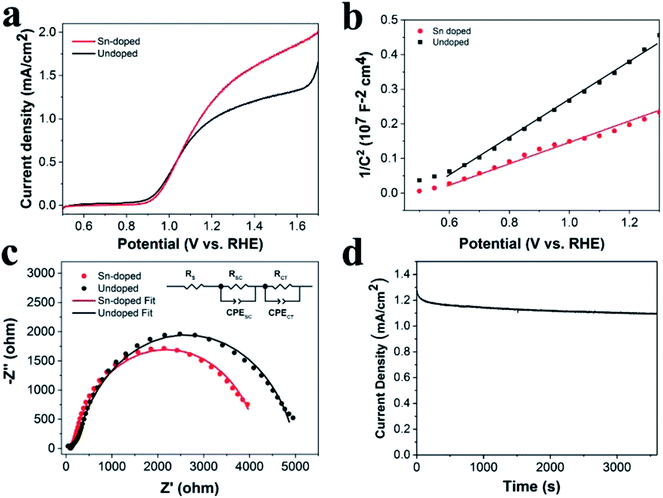
Electrochemical impedance spectroscopy (EIS) was employed to further investigate the promoting effects of the IO structure on the PEC properties, and the Nyquist plots were measured under illumination of AM 1.5G light, 100 mW cm−2, at a bias of 1.23 V vs. RHE. Fig. 4c shows typical Nyquist plots and fitted results of the ATO IO/Fe2O3 structures with different diameters and the planar control sample. The experimental data fitted well with the equivalent circuits shown in the inset, where RS is the ohmic contribution, RSC at high frequency region indicates the charge-transfer resistance at the counter electrode/electrolyte interface,44 RCT in the low frequency region correlates with the semiconductor/electrolyte charge transfer resistance, and CPESC and CPECT represent the corresponding constant phase elements of the device, respectively.5 The fitted values of the different resistances are shown in Table 1. The Nyquist plots contained two arcs for all the samples, and the large arcs in the low frequency region correspond to the charge-recombination resistance at the Fe2O3/electrolyte interface. It is obvious that the ATO IO/Fe2O3 samples had much smaller RSC and RCT values than the planar control, which confirms that both the RSC and RCT values can be decreased by the introduction of IO structures. Moreover, the RCT values of ATO IO/Fe2O3 with different diameters were different; the RCT value of the ATO IO(330)/Fe2O3 film was the lowest, followed by those of ATO IO(220)/Fe2O3 and ATO IO(670)/Fe2O3 in the stated sequence, which is consistent with the J–V curves. This confirms that the ATO IO/Fe2O3 samples with suitable diameters show improved conductivity and decreased bulk recombination. This result further explains the enhanced PEC performance of the ATO IO(330)/Fe2O3 samples.
| RS (Ω) | RSC (Ω) | RCT (Ω) | |
|---|---|---|---|
| ATO IO(220)/Fe2O3 | 12.43 | 88.69 | 6191 |
| ATO IO(330)/Fe2O3 | 11.36 | 89.74 | 4907 |
| ATO IO(670)/Fe2O3 | 10.56 | 87.44 | 9481 |
| Planar ATO/Fe2O3 | 20.33 | 228.5 | 23![[thin space (1/6-em)]](https://www.rsc.org/images/entities/char_2009.gif) 390 390 |
Incident photo-to-current conversion efficiency (IPCE) measurements were carried out on ATO IO(330)/Fe2O3 at 1.23 V vs. RHE. The IPCE was calculated from eqn (2):
| IPCE = (1240I)/(λJlight) | (2) |
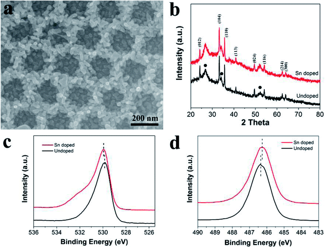
Previous studies revealed that the photoelectrochemical performance of hematite can be effectively enhanced by doping with high valent ions, such as Sn4+ and Ti4+. Herein, to further enhance the PEC activity of ATO IO/Fe2O3, a Sn-doped ATO IO/Fe2O3 film was prepared by following the same experimental procedure except that ATO IO/FeOOH was immersed in SnCl4–ethanol solution before annealing. Fig. 5a shows the top FESEM images of the Sn-doped ATO IO(330)/Fe2O3 film. The IO structure of the sample was well arranged and the Fe2O3 nanoparticles were evenly covered on the ATO IO wall. The morphology of the Sn-doped ATO IO/Fe2O3 film was almost identical to that of the undoped ATO IO/Fe2O3 structure, which indicates that Sn-doping did not affect the morphology of the as-prepared ATO IO/Fe2O3 structure. To investigate the crystal structure and possible phase changes of the sample during Sn-doping, the Sn-doped ATO IO/Fe2O3 sample was examined by X-ray diffraction, and the spectrum was compared with that of the undoped sample, as shown in Fig. 5b. The spectra of both samples were quite similar; they exhibited typical polycrystalline rutile SnO2 phase (JCPDS no. 41-1445) and hematite phase (JCPDS no. 33-0664). The diffraction peaks of hematite in the doped sample showed no observable shifts compared to the undoped sample, suggesting that the main crystal structure of hematite was not affected during doping.
In order to investigate the composition of the sample after Sn-doping, XPS measurements of the Sn-doped ATO IO/Fe2O3 sample were conducted; the high resolution O 1s spectra and Sn 3d spectra of the Sn-doped and undoped samples are shown in Fig. 5c and d, respectively. As shown in Fig. 5c, the peak of O 1s at a binding energy of ≈530.0 eV of the Sn-doped ATO IO/Fe2O3 sample showed a slight red shift compared to that of the undoped sample (≈529.8 eV), which is consistent with the lower electron density around O after Sn-doping.45,46 On the other hand, as shown in Fig. 5d, the Sn-doped ATO IO/Fe2O3 sample showed a lower Sn 3d5/2 peak at a binding energy of around 486.3 eV. This blue shift of the binding energy peak can be attributed to the incorporation of Sn into the FeO structure.18 Based on the above analysis, Sn ions were successfully doped into the hematite structure, and the Sn-doping process did not affect the morphology of the ATO IO/Fe2O3 sample. Fig. S1 in the ESI† shows the diffuse reflectance UV-vis spectra and corresponding Tauc plots of the Sn-doped and undoped ATO IO(330)/Fe2O3 samples and the planar control sample. The diffuse reflectance UV-vis spectra shown in Fig. S1a† reveal that the absorbance of the ATO IO(330)/Fe2O3 structure was obviously enhanced compared to that of the planar control, which is in accordance with previous results and analysis. In the meantime, Sn-doping showed no obvious influence on the absorbance, which indicates that Sn-doping did not affect the morphology of the ATO IO/Fe2O3 structure. The bandgaps obtained from the Tauc plots slightly decreased from 2.06 eV for the planar control sample to 2.05 eV and 2.04 eV for the undoped and Sn-doped ATO IO(330)/Fe2O3 samples, respectively (Fig. S1b†). This slight change in the bandgap implies that the Sn-doping level in our experiment is relatively low and has little influence on the bandgap energy of Fe2O3.8,18
To investigate the photoelectrochemical behavior of the Sn-doped ATO IO/Fe2O3 structure, the LSV of the Sn-doped ATO IO(330)/Fe2O3 photoanode was measured under the same experimental conditions as the previous tests and compared with that of the undoped sample, as shown in Fig. 6a. It is obvious that the Sn-doped sample exhibited a significantly enhanced current density of 1.28 mA cm−2 at 1.23 V vs. RHE compared to that of the undoped sample (1.04 mA cm−2 at 1.23 V vs. RHE). Approximately 23% enhancement was achieved by Sn-doping. To probe the PEC enhancement mechanism of Sn-doping, Mott–Schottky plots and EIS measurements of Sn-doped ATO IO(330)/Fe2O3 sample were examined, as shown in Fig. 6b and c.
The Mott–Schottky plots (M–S plots) were employed to investigate the effects of Sn-doping on the electrochemical properties of the ATO IO/Fe2O3 sample. As shown in Fig. 6b, the M–S plots of the Sn-doped and undoped ATO IO(330)/Fe2O3 samples were measured in the dark at a frequency of 1 kHz. The positive slopes of the M–S plots indicated that both samples are n-type semiconductors, which is consistent with previous reports.12 On the other hand, M–S plots can give information about the donor densities by the Mott–Schottky equation:
 | (3) |
In addition, Fig. 6d shows the photocurrent density of the Sn-doped ATO IO(330)/Fe2O3 sample over time at 1.23 V vs. RHE under AM 1.5G illumination (100 mW cm−2) in 1 M NaOH electrolyte. As a result, the Sn-doped ATO IO(330)/Fe2O3 photoanode exhibits only a slight decay in the photocurrent density over 3600 s, which implies that the as-prepared heterostructures are highly stable chemically and optically.
We compared the PEC performance of several Fe2O3-based nanostructured photoanodes, and the results are listed in Table S1.† Among the Sn-doped hematite nanostructures and Fe2O3/conductive inverse opal heterostructures, the PEC performance of the as-prepared Sn-doped ATO IO(330)/Fe2O3 photoanode was superior. The highly conductive ATO IO provides fast charge transfer paths and enhanced light absorbance ability, while Sn-doping enhanced the conductivity of Fe2O3. The combination of two strategies in our heterostructures resulted in a higher photocurrent than those of similar reported Fe2O3-based photoanodes.16,28,31,36,48–50 Although the PEC performance of the as-prepared Sn-doped ATO IO/Fe2O3 heterostructures is not superior, the utilization of the conductive IO structure, especially the discussion of the influence of the pore sizes of IO structures, provides a novel concept and a basic reference for improvement of the PEC performance of Fe2O3 and other semiconductors.
Conclusions
In summary, we have designed and fabricated novel ATO IO/Fe2O3 heterostructures using colloidal crystals as templates, and their PEC properties were thoroughly studied. By using colloidal crystal templates with different diameters, we could controllably tune the diameters of the ATO IO/Fe2O3 heterostructures. The as-prepared ATO IO/Fe2O3 heterostructures exhibit enhanced PEC properties compared to the planar ATO/Fe2O3 reference sample. This significant enhancement is ascribed to the high conductivity of the ATO skeleton as well as the high specific area and good light harvesting properties of the 3D IO structures. In particular, the diameters of the ATO IO skeletons could affect the optical and electrical properties of the ATO IO/Fe2O3 heterostructures and hence affect their PEC properties. Moreover, the PEC properties of the ATO IO/Fe2O3 heterostructures could be further enhanced by Sn-doping. Under optimal conditions, the photocurrent density of Sn-doped ATO IO/Fe2O3 reached 1.28 mA cm−2 at 1.23 V vs. RHE, and the enhancing mechanism of Sn-doping was studied. Overall, our study suggests that the IO skeleton can enhance the PEC properties of photoanodes, and morphology tuning by controlling repetitive periods can further elevate PEC properties via optimizing light harvesting and charge transfer properties. This research and strategy may provide a new route to design and optimize nanostructured photoanodes by morphology tuning and engineering.Conflicts of interest
There are no conflicts to declare.Acknowledgements
This study was financially supported by the National Natural Science Foundation of China (Grant No. 21503085 and 21603079), the Natural Science Foundation of Hubei Province (Grant No. 2015CFB233 and 2015CFB175), the open funds of the State Key Laboratory of Agricultural Microbiology (Grant No. AMLKF201507), and the Da Bei Nong Group Promoted Project for Young Scholar of HZAU (Grant No. 2017DBN010).Notes and references
- M. Grätzel, Nature, 2001, 414, 338 CrossRef PubMed.
- K. Sivula and R. van de Krol, Nat. Rev. Mater., 2016, 1, 15010 CrossRef CAS.
- A. Fujishima and K. Honda, Nature, 1972, 238, 37 CrossRef CAS PubMed.
- T. Ling, S. A. Kulinich, Z.-L. Zhu, S.-Z. Qiao and X.-W. Du, Adv. Funct. Mater., 2014, 24, 707–715 CrossRef CAS.
- G. Yun, M. Balamurugan, H.-S. Kim, K.-S. Ahn and S. H. Kang, J. Phys. Chem. C, 2016, 120, 5906–5915 CrossRef CAS.
- L. Zhou, C. Zhao, B. Giri, P. Allen, X. Xu, H. Joshi, Y. Fan, L. V. Titova and P. M. Rao, Nano Lett., 2016, 16, 3463–3474 CrossRef CAS PubMed.
- A. B. Murphy, P. R. F. Barnes, L. K. Randeniya, I. C. Plumb, I. E. Grey, M. D. Horne and J. A. Glasscock, Int. J. Hydrogen Energy, 2006, 31, 1999–2017 CrossRef CAS.
- S. Kment, F. Riboni, S. Pausova, L. Wang, L. Wang, H. Han, Z. Hubicka, J. Krysa, P. Schmuki and R. Zboril, Chem. Soc. Rev., 2017, 46, 3716–3769 RSC.
- K. Sivula, R. Zboril, F. Le Formal, R. Robert, A. Weidenkaff, J. Tucek, J. Frydrych and M. Grätzel, J. Am. Chem. Soc., 2010, 132, 7436–7444 CrossRef CAS PubMed.
- A. G. Tamirat, J. Rick, A. A. Dubale, W.-N. Su and B.-J. Hwang, Nanoscale Horiz., 2016, 1, 243–267 RSC.
- B. Iandolo, B. Wickman, I. Zorić and A. Hellman, J. Mater. Chem. A, 2015, 3, 16896–16912 RSC.
- D.-D. Qin, Y.-L. Li, T. Wang, Y. Li, X.-Q. Lu, J. Gu, Y.-X. Zhao, Y.-M. Song and C.-L. Tao, J. Mater. Chem. A, 2015, 3, 6751–6755 RSC.
- A. J. Abel, I. Garcia-Torregrosa, A. M. Patel, B. Opasanont and J. B. Baxter, J. Phys. Chem. C, 2015, 119, 4454–4465 CrossRef CAS.
- C. Han-Wei, F. Yanming, L. Wan-Yi, L. Ying-Rui, H. Yu-Cheng, C. Jeng-Lung, C. Chi-Liang, C. Wu Ching, C. Jin-Ming, L. Jyh-Fu, S. Shaohua and D. Chung-Li, Nanotechnology, 2018, 29, 064002 CrossRef PubMed.
- A. Annamalai, P. S. Shinde, T. H. Jeon, H. H. Lee, H. G. Kim, W. Choi and J. S. Jang, Sol. Energy Mater. Sol. Cells, 2016, 144, 247–255 CrossRef CAS.
- M. Li, Y. Yang, Y. Ling, W. Qiu, F. Wang, T. Liu, Y. Song, X. Liu, P. Fang, Y. Tong and Y. Li, Nano Lett., 2017, 17, 2490–2495 CrossRef CAS PubMed.
- W.-W. Wang and J.-L. Yao, Mater. Res. Bull., 2012, 47, 1762–1767 CrossRef CAS.
- L. Xi, S. Y. Chiam, W. F. Mak, P. D. Tran, J. Barber, S. C. J. Loo and L. H. Wong, Chem. Sci., 2013, 4, 164–169 RSC.
- T. H. Jeon, A. D. Bokare, D. S. Han, A. Abdel-Wahab, H. Park and W. Choi, Appl. Catal., B, 2017, 201, 591–599 CrossRef CAS.
- L. Yichuan and L. Yat, Part. Part. Syst. Charact., 2014, 31, 1113–1121 CrossRef.
- S. Shen, S. A. Lindley, X. Chen and J. Z. Zhang, Energy Environ. Sci., 2016, 9, 2744–2775 RSC.
- V. O. Williams, E. J. DeMarco, M. J. Katz, J. A. Libera, S. C. Riha, D. W. Kim, J. R. Avila, A. B. F. Martinson, J. W. Elam, M. J. Pellin, O. K. Farha and J. T. Hupp, ACS Appl. Mater. Interfaces, 2014, 6, 12290–12294 CrossRef CAS PubMed.
- Y.-F. Xu, H.-S. Rao, X.-D. Wang, H.-Y. Chen, D.-B. Kuang and C.-Y. Su, J. Mater. Chem. A, 2016, 4, 5124–5129 RSC.
- Z. Zhang, C. Gao, Y. Li, W. Han, W. Fu, Y. He and E. Xie, Nano Energy, 2016, 30, 892–899 CrossRef CAS.
- K. Kim, I.-H. Kim, K.-Y. Yoon, J. Lee and J.-H. Jang, J. Mater. Chem. A, 2015, 3, 7706–7709 RSC.
- Y. Qiu, S.-F. Leung, Q. Zhang, B. Hua, Q. Lin, Z. Wei, K.-H. Tsui, Y. Zhang, S. Yang and Z. Fan, Nano Lett., 2014, 14, 2123–2129 CrossRef CAS PubMed.
- H. Hyungkyu, K. Stepan, K. Frantisek, W. Lei, N. Alberto, S. Patrik and Z. Radek, Small, 2018, 14, 1703860 CrossRef PubMed.
- X. Yang-Fan, R. Hua-Shang, C. Bai-Xue, L. Ying, C. Hong-Yan, K. Dai-Bin and S. Cheng-Yong, Adv. Sci., 2015, 2, 1500049 CrossRef PubMed.
- L. N. Quan, Y. H. Jang, K. A. Stoerzinger, K. J. May, Y. J. Jang, S. T. Kochuveedu, Y. Shao-Horn and D. H. Kim, Phys. Chem. Chem. Phys., 2014, 16, 9023–9030 RSC.
- Y. Yu, J. Quan, M. Dan, Q. Jian, W. Yanze, Y. Ranbo, L. Anran, L. Shuzhou, Z. Huijun, M. Yanwen, W. Lianhui, H. Wenping and W. Dan, Adv. Mater., 2017, 29, 1604795 CrossRef PubMed.
- C. Xiaobo, Z. Haifeng and C. Chuanwei, Semicond. Sci. Technol., 2017, 32, 114003 CrossRef.
- K. Yu, C. Zhang, Y. Chang, Y. Feng, Z. Yang, T. Yang, L.-L. Lou and S. Liu, Appl. Catal., B, 2017, 200, 514–520 CrossRef CAS.
- M. Zhou, J. Bao, Y. Xu, J. Zhang, J. Xie, M. Guan, C. Wang, L. Wen, Y. Lei and Y. Xie, ACS Nano, 2014, 8, 7088–7098 CrossRef CAS PubMed.
- Y. Gun, G. Y. Song, V. H. V. Quy, J. Heo, H. Lee, K.-S. Ahn and S. H. Kang, ACS Appl. Mater. Interfaces, 2015, 7, 20292–20303 CrossRef CAS PubMed.
- M. Ma, J. K. Kim, K. Zhang, X. Shi, S. J. Kim, J. H. Moon and J. H. Park, Chem. Mater., 2014, 26, 5592–5597 CrossRef CAS.
- K.-Y. Yoon, J.-S. Lee, K. Kim, C. H. Bak, S.-I. Kim, J.-B. Kim and J.-H. Jang, ACS Appl. Mater. Interfaces, 2014, 6, 22634–22639 CrossRef CAS PubMed.
- I. Kondofersky, H. K. Dunn, A. Müller, B. Mandlmeier, J. M. Feckl, D. Fattakhova-Rohlfing, C. Scheu, L. M. Peter and T. Bein, ACS Appl. Mater. Interfaces, 2015, 7, 4623–4630 CrossRef CAS PubMed.
- P. Jiang, J. F. Bertone, K. S. Hwang and V. L. Colvin, Chem. Mater., 1999, 11, 2132–2140 CrossRef CAS.
- L. Vayssieres, N. Beermann, S.-E. Lindquist and A. Hagfeldt, Chem. Mater., 2001, 13, 233–235 CrossRef CAS.
- A. M. Xavier, F. F. Ferreira and F. L. Souza, RSC Adv., 2014, 4, 17753–17759 RSC.
- X. Chen, J. Ye, S. Ouyang, T. Kako, Z. Li and Z. Zou, ACS Nano, 2011, 5, 4310–4318 CrossRef CAS PubMed.
- K. Kim, P. Thiyagarajan, H.-J. Ahn, S.-I. Kim and J.-H. Jang, Nanoscale, 2013, 5, 6254–6260 RSC.
- Q. Zeng, J. Bai, J. Li, L. Xia, K. Huang, X. Li and B. Zhou, J. Mater. Chem. A, 2015, 3, 4345–4353 RSC.
- Y. Zhang, J. Cai, Y. Ma and L. Qi, Nano Res., 2017, 10, 2610–2625 CrossRef CAS.
- V. Müller, M. Rasp, G. Štefanić, J. Ba, S. Günther, J. Rathousky, M. Niederberger and D. Fattakhova-Rohlfing, Chem. Mater., 2009, 21, 5229–5236 CrossRef.
- K. L. Purvis, G. Lu, J. Schwartz and S. L. Bernasek, J. Am. Chem. Soc., 2000, 122, 1808–1809 CrossRef CAS.
- M. Ji, J. Cai, Y. Ma and L. Qi, ACS Appl. Mater. Interfaces, 2016, 8, 3651–3660 CrossRef CAS PubMed.
- A. Subramanian, E. Gracia-Espino, A. Annamalai, H. H. Lee, S. Y. Lee, S. H. Choi and J. S. Jang, Appl. Surf. Sci., 2018, 427, 1203–1212 CrossRef CAS.
- J.-J. Wang, Y. Hu, R. Toth, G. Fortunato and A. Braun, J. Mater. Chem. A, 2016, 4, 2821–2825 RSC.
- S. C. Riha, M. J. DeVries Vermeer, M. J. Pellin, J. T. Hupp and A. B. F. Martinson, ACS Appl. Mater. Interfaces, 2013, 5, 360–367 CrossRef CAS PubMed.
Footnote |
| † Electronic supplementary information (ESI) available. See DOI: 10.1039/c8ra06504g |
| This journal is © The Royal Society of Chemistry 2018 |

