
 Open Access Article
 This Open Access Article is licensed under a Creative Commons Attribution-Non Commercial 3.0 Unported Licence
Synthesis of a one-dimensional atomic crystal of vanadium selenide (V2Se9)†
Seungbae
Oh‡
a,
Sudong
Chae‡
a,
Bum Jun
Kim
b,
Kyung Hwan
Choi
b,
Woo-Sung
Jang
c,
Jimin
Jang
b,
Yasmin
Hussain
a,
Dong Kyu
Lee
d,
Young-Min
Kim
 ce,
Hak Ki
Yu
*d and
Jae-Young
Choi
*ab
ce,
Hak Ki
Yu
*d and
Jae-Young
Choi
*ab
aSchool of Advanced Materials Science & Engineering, Sungkyunkwan University, Suwon 16419, Republic of Korea. E-mail: jy.choi@skku.edu
bSKKU Advanced Institute of Nanotechnology (SAINT), Sungkyunkwan University, Suwon 16419, Republic of Korea
cDepartment of Energy Science, Sungkyunkwan University, Suwon 16419, Republic of Korea
dDepartment of Materials Science and Engineering, Department of Energy Systems Research, Ajou University, Suwon 16499, Republic of Korea. E-mail: hakkiyu@ajou.ac.kr
eCenter for Integrated Nanostructure Physics, Institute for Basic Science (IBS), Suwon 16419, Republic of Korea
First published on 3rd October 2018
Abstract
The synthesis and nanoscale dispersion of a new one-dimensional (1D) material, V2Se9, in which chain-shaped molecular units with strong covalent bonds are assembled in a crystal structure via weak van der Waals attraction between chains, were successfully carried out. V2Se9 is synthesized by solid-state reaction and additional heat treatment. The synthesized V2Se9 has excellent thermal stability up to 400 °C and has been experimentally confirmed to be dispersed up to ∼20 nm or less through a specific solvent dispersion. The covalently bonded V2Se9 chain, when isolated from its bulk material, is expected to exhibit unique quantum physical properties owing to the confinement of electrons in the 1D chain structure and the absence of inter-chain interactions, as demonstrated in the case of graphene and other 2D materials. Therefore, the novel 1D material of V2Se9, as an extension of the current 2D material, is expected to create a new class of materials that will be of significant interest to the materials science and nanotechnology communities for new device applications.
Introduction
Scaling down or size-reduction has been one of the important aspects of modern science and technology for the development of devices with higher performance. To overcome the problems of existing materials occurring in nano-size, there has been a paradigm shift in research towards low-dimensional (2D and 1D) materials. Unlike the nanomaterials obtained by merely reducing the size of bulk materials, low-dimensional materials present new quantum-physical characteristics and excellent electrical, optical, and mechanical properties.1–9Among the 2D materials, graphene exhibits excellent carrier mobility, but does not have the bandgap necessary for the fabrication of reliable semiconductor devices.10 Other 2D semiconductor materials, such as transition metal dichalcogenides (TMDCs) and black phosphor, have appropriate bandgaps (1–2 eV), but their stability and/or carrier mobility are limited.11–13 More importantly, decreased transport properties at the nanoscale are still unavoidable in current 2D materials, because they have dangling bonds at the side edges and domain boundaries.14 Carbon nanotubes (CNTs, representative 1D materials), which exhibit high electrical mobility, chemical stability, and mechanical strength, have been extensively studied for use as building blocks of transistors, sensors, and nanocomposites.15–17 However, the wide range of electronic structures that arise from the different chirality of CNTs hinders the fabrication of nanoelectronic devices with uniform performance. Therefore, it is necessary to either achieve separation of single-chirality CNTs from bulk CNTs or control the chirality during the growth of CNTs.18 Although several studies have addressed these issues, it is still challenging to obtain single-chirality CNTs.
To overcome the problems of existing low-dimensional materials, researches on new 1D materials have been carried out. For example, extensive studies for bulk synthesis and atomic scale dispersion of LiMo3Se3 and Mo6S9−xIx have been reported.19–33 Recently, quantum confinement effect of LiMo3Se3 and bio-stability of Mo6S9−xIx were demonstrated and their applications have been explored.24,25,29,33 In addition, device application using new 1D materials, such as Sb2Se3 (optoelectronic devices using the property of effectively reducing exciton decay because of absence of dangling bonds) and VS4 (electrochemical energy storage using the space between 1D nanostructures) have been reported.34–36 Therefore, there is a definite scope for identification, synthesis, and characterization of new 1D materials.
By understanding the mechanism by which 1D materials form a 3D structure, new 1D materials can be discovered for potential applications. As the interlayer coupling energy of 2D materials is categorized into van der Waals (vdW) bonding and electrostatic bonding, the above-mentioned new 1D materials can also be classified accordingly: vdW bonding in Sb2Se3, Mo6S9−xIx, and VS4 and electrostatic bonding by intercalated Li+ in LiMo3Se3. In the case of cation intercalated 1D materials, cations are separated in the process of dispersion,24 leaving a local negative charge defect on the surface of the 1D materials.19–23 On the other hand, in the case of vdW bonding, it is advantageous to obtain a high-purity 1D atomic crystal without surface defects using an appropriate synthesis process. Among the 1D materials with vdW type bonds, the synthesis, dispersion, and basic properties of Mo6S9−xIx have been studied to a relatively significant degree.26–29,31–33 However, the crystal structure of Mo6S9−xIx has not been well-defined since the positions of sulfur and iodine atoms bridged to molybdenum atoms may vary even in the same stoichiometric composition. In addition, the thermodynamic information of the ternary system (Mo, S, and I) is also lacking, which makes it difficult to understand the physical properties of Mo6S9−xIx.30
In this study, we have synthesized a new 1D bulk material with a binary system and well-defined crystal structure, V2Se9, in which chain-shaped molecular units with strong covalent bonds are assembled in a crystal structure via weak vdW attraction between chains. In addition, 1D materials with an inorganic molecular chain structure and dangling bond-free surface were obtained as a single-chain atomic crystal from a 3D bulk solid by the dispersion based exfoliation method (see Fig. 1a).
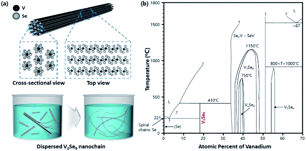 | ||
| Fig. 1 (a) Crystal structure of V2Se9 and schematic illustration of the V2Se9 dispersion. (b) Phase diagram of V–Se binary system. | ||
Results and discussion
As shown in the phase diagram in Fig. 1b, vanadium, transition metal with an outermost 3d orbital, can bond with selenium in various compositions (from V5Se4 to V2Se9). Therefore, to synthesize a stoichiometric V2Se9 compound, the V![[thin space (1/6-em)]](https://www.rsc.org/images/entities/char_2009.gif) :Se ratio and the synthesis temperature need to be carefully considered. When the synthesis of V and Se powders in solid form is carried out at an exact atomic mixing ratio of 2:9, an unwanted phase (VSe2) can be formed at the specific interface owing to fluctuations in the V:Se ratio. Therefore, in this study, the experiment was carried out under excess Se conditions (V:Se ratio of 2:12.6). The experimental results obtained for the exact stoichiometric ratio of 2:9 are shown in Fig. S2.†
:Se ratio and the synthesis temperature need to be carefully considered. When the synthesis of V and Se powders in solid form is carried out at an exact atomic mixing ratio of 2:9, an unwanted phase (VSe2) can be formed at the specific interface owing to fluctuations in the V:Se ratio. Therefore, in this study, the experiment was carried out under excess Se conditions (V:Se ratio of 2:12.6). The experimental results obtained for the exact stoichiometric ratio of 2:9 are shown in Fig. S2.†
The results of X-ray diffraction (XRD) analysis of the samples synthesized at different temperatures (Fig. 2a) indicate that the V2Se9 phase is formed at temperatures below 330 °C, whereas the VSe2 phase is formed at temperatures above 360 °C (mixed phase at 340 °C). Scanning electron microscopy (SEM) and energy dispersive spectroscopy (EDS) were performed to analyze the structure and the composition of the materials synthesized at three specific temperatures (330, 340, and 380 °C). Using the results of XRD and EDS composition analysis, it is possible to determine the composition of the microstructural region at each temperature (Fig. 2b and S2†). The VSe2 phase appears at 380 °C and shows a layered lamellar structure, which is similar to the previously reported structure of TMDCs.37 The V2Se9 phase, which appears at temperatures ≤ 340 °C, exhibits a 3D structure. However, as can be seen from the SEM images at 340 °C, a part of the V2Se9 phase begins to partially disperse into a 1D structure like a thread. Furthermore, Se, which is observed at all temperatures, is dispersed in several places in the form of particles; Se can be removed by heat treatment at its sublimation temperature (>221 °C).38
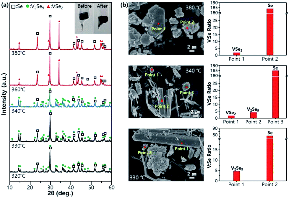 | ||
| Fig. 2 (a) XRD patterns (inset is the optical images of sample before and after reaction) and (b) SEM images (left) and EDS analysis (right) of as-synthesized samples with T ranging from 320 °C to 380 °C. (V:Se ratio is 2:12.6). | ||
The remaining Se particles can be removed by sublimation (heat treatment in a tube furnace at 250 °C under Ar atmosphere for 24 h). It is evident from the XRD pattern (Fig. 3a) that, Se with hexagonal crystals in the solid state can be completely removed after sublimation, and the V2Se9 solid crystal is exposed at the site where Se is sublimated (Fig. 3b). The thermal stability and the residual Se sublimation of V2Se9 were confirmed by thermogravimetric characterization using differential thermal analysis (DTA) and thermogravimetric analysis (TGA) (Fig. 3c and d). Before Se sublimation treatment, the mass decrease was about 68.1%, while that after Se sublimation treatment was 46.5%. Mass reduction occurs even after Se sublimation, because the decomposition process (V2Se9(s) → 2VSe2(S) + 5Se(g)) happens at approximately 400 °C. In other words, the V2Se9 samples synthesized in this experiment show stable thermal properties up to 400 °C. Also, after Se sublimation, the exothermic DTA peaks at approximately 400 °C is evident along with decomposition of V2Se9 into VSe2 and Se. Otherwise, in the DTA curves before Se sublimation, exothermic peaks from decomposition reaction (V2Se9(s) → 2VSe2(S) + 5Se(g)) is cancelled out by the endothermic Se sublimation reaction.
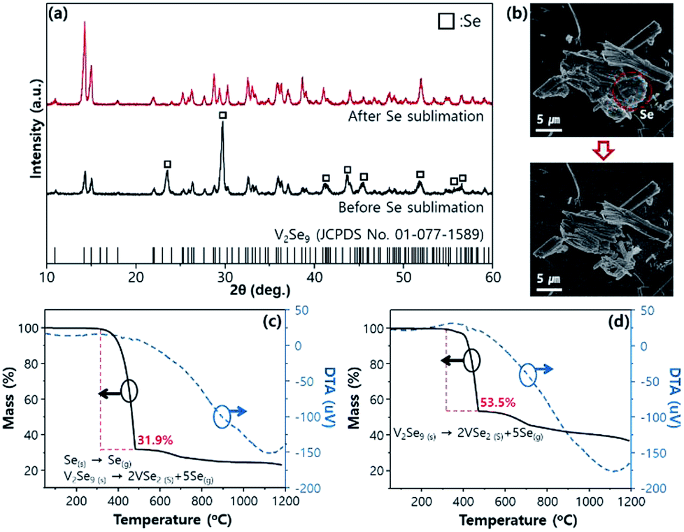 | ||
| Fig. 3 Physical and chemical changes of V2Se9 synthesized at 330 °C after Se sublimation. (a) XRD patterns (bottom: before Se sublimation, top: after Se sublimation), (b) SEM images (top: before Se sublimation, bottom: after Se sublimation, red dashed circle is Se) and (c and d) TG/DTA analysis in N2 atmosphere (left: before Se sublimation, right: after Se sublimation, red dashed line is Se sublimation and V2Se9 decomposition step). | ||
The residual-Se sublimated V2Se9 was dispersed into a 1D chain and its characteristics were analyzed. Bulk V2Se9 was dispersed in isopropyl alcohol (IPA) solvent and deposited on Si/SiO2 wafer after sonication. As shown in Fig. 4a, a distinctive Tyndall effect appears, indicating nanoscale dispersion. The dispersed V2Se9 in IPA were spin-coated on Si/SiO2 substrates, and the size of the nano-chain was analyzed using an atomic force microscope (AFM); the results are shown in Fig. 4b. It is evident that the 1D structure of V2Se9 chains with an average size of 16 nm is well dispersed. IR absorption spectrum of dispersed solution is given in Fig. S3.† The IR absorption peak is observed at 1700 nm which correspond to the known bandgap of 0.73 eV (Fig. S3†). Transmission electron microscopy (TEM) results also confirm that the 1D chain of size 16 nm exhibits a high degree of crystallinity and is well separated (Fig. 4c). It is considered that more detailed separation of 1D V2Se9 chains into atomic units will require optimization of the dispersion solvent and the dispersion process.
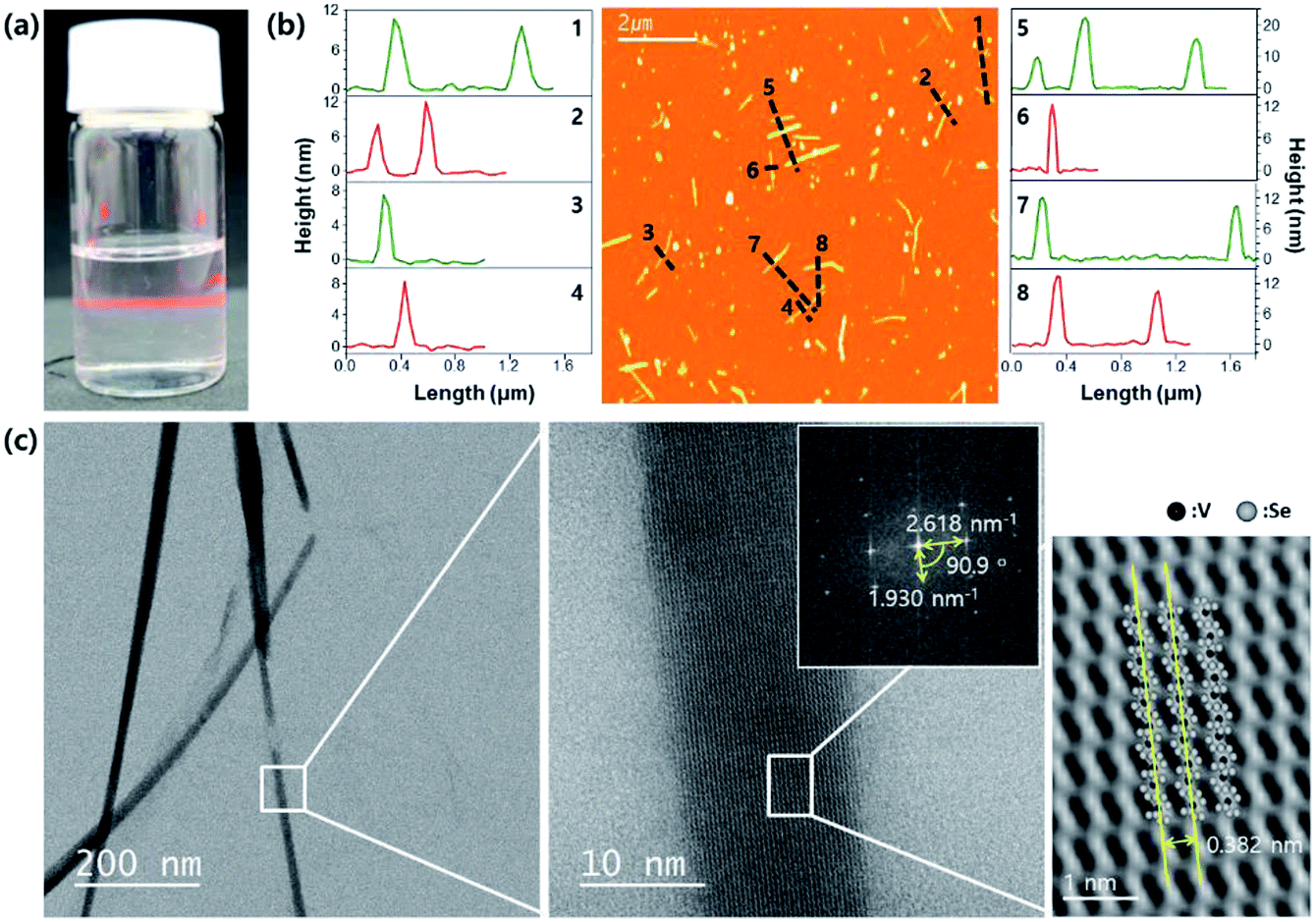 | ||
| Fig. 4 Dispersion of V2Se9 in IPA. (a) Tyndall effect of V2Se9 dispersed solution. (b) AFM image of V2Se9 chains deposited on Si/SiO2 substrate and the height profiles along each dashed line. (c) TEM images and FFT pattern (inset) of dispersed V2Se9 chains (the distance between two chains marked by yellow line is 0.382 nm). | ||
Experimental section
Synthesis
Vanadium selenide (V2Se9) was synthesized using V (powder, –325 mesh, 99.5%, Aldrich) and Se (powder, 99+%, Alfa Aesar) elements. The mixture of V (0.2038 g) and Se (1.4213 or 1.9898 g for V:Se ratio of 2:9 or 2:12.6) was pelletized and then sealed in a 10 cm-long evacuated quartz tube. The quartz ampoule was heated for 120 h at a temperature of 300–400 °C (at 5.5 °C h−1) and then cooled (at 10 °C h−1). The resulting material was a dark gray sintered powder (right inset, Fig. 2a). The unreacted Se was sublimated in a tube furnace at 250 °C under Ar atmosphere for 24 h.
Dispersion
Two milligrams of V2Se9 were dispersed in 20 mL of IPA by ultrasonication. The ultrasonication was implemented by probe sonication (VC 505, Sonics & Materials, Inc.) for 5 min at a 2 s on/2 s off interval in order to crush the chunk powders. Then, bath sonication was implemented (B2005S-68K, 68 kHz, 200 W, KODO Technical) for 3 h to exfoliate the crushed bulk V2Se9 into nanochain as well as prevent the damage from probe sonication.39,40 After ultrasonication, centrifugation at 6000 rpm for 10 min was carried out to remove the insufficiently dispersed chains. Five milliliters of the supernatant solution was used for AFM and TEM analyses.Characterization
Powder XRD (Mac Science, M18XHF22) was performed using Cu-Kα radiation (λ = 0.154 nm). A field-emission scanning electron microscope (FESEM, Hitachi, S-4300SE) and EDS attached to FESEM was employed for morphology and composition analysis. Thermal gravimetry differential thermal analysis (TG-DTA, Seiko Instrument Inc., TG/DTA7300) measurements were performed under N2 atmosphere up to 1200 °C (at 10 °C min−1). Atomic force microscopy (AFM, Park systems, XE100 & XE150) was operated in non-contact mode; the samples were prepared by spin coating on Si/SiO2 wafer. UV-vis-NIR spectroscopy (Agilent Technologies, CARY-5000) was employed for the optical property analysis. An aberration-corrected scanning transmission electron microscope (STEM, JEOL, JEM ARM 200F) was operated at an acceleration voltage of 80 kV. The sample for STEM was prepared by drop casting on a graphene-coated Quantifoil TEM grid.Conclusions
The synthesis and nanoscale dispersion of a new 1D material, V2Se9, which exhibits a molecular chain structure with a diameter up to ∼1 nm, were successfully carried out. The reaction of V and Se was induced by the solid-state method to synthesize high purity V2Se9 crystals. The synthesized V2Se9 crystals were dispersed to obtain 1D nanochains with a size of 16 nm or less. The covalently bonded V2Se9 chain, when isolated from its 3D bulk material, is expected to exhibit unique quantum physical properties owing to the confinement of electrons in the 1D chain structure and the absence of inter-chain interactions, as demonstrated in the case of graphene and other 2D materials.1,2 Therefore, the novel 1D material of V2Se9, as an extension of the current 2D material, is expected to create a new class of materials that will be of significant interest to materials science and nanotechnology communities for new device applications.Author contribution
J. Y. C. designed the experiments, and S. O. and S. C. performed the chemical reaction experiments and B. J. K. and K. H. C. supported the elemental analysis. J. J. and Y. H. support the chemical reaction experiment and D. K. and W. S. J. and Y. M. K. supported structural analysis. H. K. Y. and J. Y. C. conceived and supervised this study and provided intellectual and technical guidance”.Conflicts of interest
There are no conflicts to declare.Acknowledgements
This research was supported by Nano Material Technology Development Program through the National Research Foundation of Korea (NRF) funded by Ministry of Science and ICT (2017M3A7B8065561). This work was supported by the National Research Foundation of Korea (NRF) grant funded by the Korea government (MSIP) (No. NRF-2017R1A4A1015770).References
- K. S. Novoselov, A. K. Geim, S. Morozov, D. Jiang, M. Katsnelson, I. Grigorieva, S. Dubonos and A. A. Firsov, Nature, 2005, 438, 197 CrossRef CAS PubMed.
- Y. Zhang, Y.-W. Tan, H. L. Stormer and P. Kim, Nature, 2005, 438, 201 CrossRef CAS PubMed.
- K. I. Bolotin, K. Sikes, Z. Jiang, M. Klima, G. Fudenberg, J. Hone, P. Kim and H. Stormer, Solid State Commun., 2008, 146, 351–355 CrossRef CAS.
- K. S. Kim, Y. Zhao, H. Jang, S. Y. Lee, J. M. Kim, K. S. Kim, J.-H. Ahn, P. Kim, J.-Y. Choi and B. H. Hong, Nature, 2009, 457, 706 CrossRef CAS PubMed.
- C. Lee, X. Wei, J. W. Kysar and J. Hone, Science, 2008, 321, 385–388 CrossRef CAS PubMed.
- G. Tai, T. Hu, Y. Zhou, X. Wang, J. Kong, T. Zeng, Y. You and Q. Wang, Angew. Chem., 2015, 127, 15693–15697 CrossRef.
- T. Hu, K. Bian, G. Tai, T. Zeng, X. Wang, X. Huang, K. Xiong and K. Zhu, J. Phys. Chem. C, 2016, 120, 25843–25850 CrossRef CAS.
- Z. Wu, G. Tai, X. Wang, T. Hu, R. Wang and W. Guo, Nanotechnology, 2018, 29, 125605 CrossRef PubMed.
- G. Tai, T. Zeng, J. Yu, J. Zhou, Y. You, X. Wang, H. Wu, X. Sun, T. Hu and W. Guo, Nanoscale, 2016, 8, 2234–2241 RSC.
- B. Radisavljevic, A. Radenovic, J. Brivio, i. V. Giacometti and A. Kis, Nat. Nanotechnol., 2011, 6, 147 CrossRef CAS PubMed.
- K. F. Mak, C. Lee, J. Hone, J. Shan and T. F. Heinz, Phys. Rev. Lett., 2010, 105, 136805 CrossRef PubMed.
- J. Qiao, X. Kong, Z.-X. Hu, F. Yang and W. Ji, Nat. Commun., 2014, 5, 4475 CrossRef CAS PubMed.
- A. Castellanos-Gomez, L. Vicarelli, E. Prada, J. O. Island, K. Narasimha-Acharya, S. I. Blanter, D. J. Groenendijk, M. Buscema, G. A. Steele and J. Alvarez, 2D Mater., 2014, 1, 025001 CrossRef.
- F. Schwierz, Nat. Nanotechnol., 2010, 5, 487 CrossRef CAS PubMed.
- P. Avouris, M. Freitag and V. Perebeinos, Nat. Photonics, 2008, 2, 341 CrossRef CAS.
- J. Wang and M. Musameh, Anal. Chem., 2003, 75, 2075–2079 CrossRef CAS PubMed.
- Z. Chen, V. Augustyn, J. Wen, Y. Zhang, M. Shen, B. Dunn and Y. Lu, Adv. Mater., 2011, 23, 791–795 CrossRef CAS PubMed.
- M. Kusunoki, T. Suzuki, C. Honjo, T. Hirayama and N. Shibata, Chem. Phys. Lett., 2002, 366, 458–462 CrossRef CAS.
- J. H. Golden, F. J. DiSalvo, J. M. Fréchet, J. Silcox, M. Thomas and J. Elman, Science, 1996, 273, 782–784 CrossRef CAS PubMed.
- A. Heidelberg, H. Bloess, J. Schultze, C. Booth, E. Samulski and J. Boland, Z. Phys. Chem, 2003, 217, 573–586 CrossRef CAS.
- B. Messer, J. H. Song, M. Huang, Y. Wu, F. Kim and P. Yang, Adv. Mater., 2000, 12, 1526–1528 CrossRef CAS.
- F. E. Osterloh, H. Hiramatsu, R. Dumas and K. Liu, Langmuir, 2005, 21, 9709–9713 CrossRef CAS PubMed.
- F. E. Osterloh, J. S. Martino, H. Hiramatsu and D. P. Hewitt, Nano Lett., 2003, 3, 125–129 CrossRef CAS.
- J. Tarascon, F. DiSalvo, C. Chen, P. Carroll, M. Walsh and L. Rupp, J. Solid State Chem., 1985, 58, 290–300 CrossRef CAS.
- J.-M. Tarascon, G. Hull and F. DiSalvo, Mater. Res. Bull., 1984, 19, 915–924 CrossRef CAS.
- B. Berčič, U. Pirnat, P. Kusar, D. Dvorsek, D. Mihailovic, D. Vengust and B. Podobnik, Appl. Phys. Lett., 2006, 88, 173103 CrossRef.
- J. J. Doyle, V. Nicolosi, S. M. O'Flaherty, D. Vengust, A. Drury, D. Mihailovic, J. N. Coleman and W. J. Blau, Chem. Phys. Lett., 2007, 435, 109–113 CrossRef CAS.
- Z. Kutnjak, D. Vrbanić, S. Pejovnik and D. Mihailović, J. Appl. Phys., 2006, 99, 064311 CrossRef.
- D. N. McCarthy, V. Nicolosi, D. Vengust, D. Mihailovic, G. Compagnini, W. J. Blau and J. N. Coleman, J. Appl. Phys., 2007, 101, 014317 CrossRef.
- A. Meden, A. Kodre, J. P. Gomilšek, I. Arčon, I. Vilfan, D. Vrbanic, A. Mrzel and D. Mihailovic, Nanotechnology, 2005, 16, 1578 CrossRef CAS.
- D. Vengust, F. Pfuner, L. Degiorgi, I. Vilfan, V. Nicolosi, J. Coleman and D. Mihailovic, Phys. Rev. B: Condens. Matter Mater. Phys., 2007, 76, 075106 CrossRef.
- I. Vilfan and D. Mihailovic, Phys. Rev. B: Condens. Matter Mater. Phys., 2006, 74, 235411 CrossRef.
- D. Vrbanić, M. Remškar, A. Jesih, A. Mrzel, P. Umek, M. Ponikvar, B. Jančar, A. Meden, B. Novosel and S. Pejovnik, Nanotechnology, 2004, 15, 635 CrossRef.
- Y. Zhou, L. Wang, S. Chen, S. Qin, X. Liu, J. Chen, D.-J. Xue, M. Luo, Y. Cao and Y. Cheng, Nat. Photonics, 2015, 9, 409 CrossRef CAS.
- X. Xu, S. Jeong, C. S. Rout, P. Oh, M. Ko, H. Kim, M. G. Kim, R. Cao, H. S. Shin and J. Cho, J. Mater. Chem. A, 2014, 2, 10847–10853 RSC.
- S. Britto, M. Leskes, X. Hua, C.-A. Hébert, H. S. Shin, S. Clarke, O. Borkiewicz, K. W. Chapman, R. Seshadri and J. Cho, J. Am. Chem. Soc., 2015, 137, 8499–8508 CrossRef CAS PubMed.
- S. Jeong, D. Yoo, J.-t. Jang, M. Kim and J. Cheon, J. Am. Chem. Soc., 2012, 134, 18233–18236 CrossRef CAS PubMed.
- A. A. Jadhav and P. K. Khanna, RSC Adv., 2015, 5, 44756–44763 RSC.
- Y. Xing, L. Li, C. C. Chusuei and R. V. Hull, Langmuir, 2005, 21, 4185–4190 CrossRef CAS PubMed.
- U. Khan, H. Porwal, A. O'Neill, K. Nawaz, P. May and J. N. Coleman, Langmuir, 2011, 27, 9077–9082 CrossRef CAS PubMed.
Footnotes |
| † Electronic supplementary information (ESI) available: EDS mappings of samples in Fig. 2 synthesized at 380 °C, 340 °C and 330 °C (Fig. S1), XRD patterns, SEM images and EDS analysis of as-synthesized samples with temperature ranging from 300 °C to 400 °C (Fig. S2). IR absorption spectrum of V2Se9 (Fig. S3). See DOI: 10.1039/c8ra06398b |
| ‡ S. Oh and S. Chae contributed equally to this work. |
| This journal is © The Royal Society of Chemistry 2018 |