
 Open Access Article
 This Open Access Article is licensed under a Creative Commons Attribution-Non Commercial 3.0 Unported Licence
Enhanced absorption of TiO2 nanotubes by N-doping and CdS quantum dots sensitization: insight into the structure†
Andjelika Bjelajac *a,
Rada Petrovićb,
Veljko Djokicb,
Vladimir Matolinc,
Martin Vondračekd,
Kassioge Dembeleef,
Simona Moldovaneg,
Ovidiu Ersene,
Gabriel Socolh,
Ion N. Mihailescuh and
Djordje Janaćkovićb
*a,
Rada Petrovićb,
Veljko Djokicb,
Vladimir Matolinc,
Martin Vondračekd,
Kassioge Dembeleef,
Simona Moldovaneg,
Ovidiu Ersene,
Gabriel Socolh,
Ion N. Mihailescuh and
Djordje Janaćkovićb
aUniversity of Belgrade, Innovation Center of Faculty of Technology and Metallurgy, Karnegijeva 4, 11000 Belgrade, Serbia. E-mail: abjelajac@tmf.bg.ac.rs
bUniversity of Belgrade, Faculty of Technology and Metallurgy, Karnegijeva 4, 11000 Belgrade, Serbia
cCharles University in Prague, Faculty of Mathematics and Physics, Department of Surface and Plasma Science, V Holešovičkách 2, 180 00 Prague 8, Czech Republic
dInstitute of Physics of Czech Academy of Sciences, Na Slovance 1999/2, 182 21 Prague 8, Czech Republic
eInstitut de Physique et Chimie des Materiaux de Strasbourg, UMR 7504, CNRS, Université de Strasbourg, 23 rue du Loess, BP 43, 67037 Strasbourg Cedex 02, France
fFritz Haber Institute of the Max Planck Society, Faradayweg 4, 14195 Berlin, Germany
gUniversité de Rouen, INSA Rouen, Groupe de Physique des Matériaux, UMR, CNRS 6634, Avenue de l’Université – BP12, 76801 Saint Etienne du Rouvray, France
hNational Institute for Lasers, Plasma, and Radiation Physics, Lasers Department, “Laser-Surface-Plasma Interactions” Laboratory, PO Box MG-54, RO-77125, Magurele, Ilfov, Romania
First published on 12th October 2018
Abstract
Anodization of titanium film sputtered on fluorine doped tin oxide (FTO) glass was performed to obtain highly ordered ∼2 μm long and ∼60 nm wide TiO2 nanotubes. The titania films were annealed in ammonia atmosphere to enable the doping with N. The annealing did not affect the nanotubular morphology and the porosity remained open which is a very important requirement for further deposition of CdS quantum dots. The analysis done by transmission electron microscopy (TEM) has shown that the N-doped nanotubes have a smaller interplanar distance as compared to the undoped ones, whose interplanar distance corresponded to anatase phase. This difference was attributed to the N doping and the Sn migration from the substrate, as demonstrated by energy dispersive spectroscopy (EDS) combined with electron energy loss spectroscopy (EELS). The near edge X-ray absorption fine structure (NEXAFS) analysis clearly demonstrated that also the doped TiO2 film has anatase phase. Regarding the chemical composition of the studied samples, the X-ray photoelectron spectroscopy (XPS) and synchrotron radiation photoelectron spectroscopy (SRPES) analyses have shown that N is incorporated both interstitially and substitutionally in the TiO2 lattice, with a decreased contribution of the interstitial after ionic sputtering. The shift of the valence band maximum (VBM) position for the doped TiO2 vs. the undoped TiO2 proved the narrowing of the band gap. The CdS/TiO2 films show bigger VBM shifting that can be attributed to CdS deposit. Comparing the absorption spectra of the bare undoped and doped TiO2 samples, it was noticed that the doping causes a red shift from 397 to 465 nm. Furthermore, the CdS deposition additionally enhances the absorption in the visible range (575 nm for undoped TiO2/CdS and 560 nm for doped TiO2/CdS films).
Introduction
Titanium dioxide (TiO2) is a nontoxic and photosensitive semiconductor,1 very competitive in terms of its low costs and is commonly used in the production of the third generation of solar cells.2,3 A main drawback is that it absorbs only ∼5% of the entire solar spectrum,4 which results in the low efficiency of the devices using this technology. Therefore, the scientific community has oriented its attention to the improvement of the absorption characteristics of the titania photoanode, by tailoring the chemical and morphological properties of TiO2 and/or by employing an appropriate sensitizer.5 One should note that one dimensional (1D) nanotubular structure exhibits superior characteristics as compared to nanoparticular TiO2.3 It was shown that under UV radiation the diffusion of electrons is much faster along TiO2 nanotubes (NTs) than through nanoparticles.6 Additionally, the electron transfer loss is reduced inside NTs since there are no grain boundaries as within nanoparticular TiO2.7 The structural disorder at the contact between two crystalline nanoparticles leads to enhanced scattering of free electrons, thus reducing electron mobility.8,9 Since the length of the NTs could be in micrometres the visible light scattering and absorption are improved greatly as compared to the nanoparticles.3 Among many methods that are applied for the synthesis of TiO2, the anodization was shown to be a highly reproducible and controllable technique for obtaining highly ordered TiO2 NTs arrays perpendicularly oriented to titanium substrate.10 Such orientation is advantageous as compared to nanoparticular thin film or film made of disordered NTs that lie in the plane of the substrates, since in those kinds of films there are gaps that cannot be reached by a sensitizer.3Another proposed approach to further improve the TiO2 based photoanode in terms of absorbance properties, is by doping with anions, among which N showed to be the most prominent. The doping of TiO2 NTs with N can be done by immersing of the NTs in N containing solutions,11 thermal treatment in NH3 gas atmosphere,12 sputtering in N2 atmosphere,13 high-energetic ion implantation,14 adding urea15 or NH4NO3![[thin space (1/6-em)]](https://www.rsc.org/images/entities/char_2009.gif) 16 in the electrolyte for anodization. The advantage seems to be given to the thermal treatment in NH3 atmosphere since it enables simultaneously both transformation of the anodized TiO2 NTs from amorphous to more a conductive crystalline phase and doping with N by a single step process.
16 in the electrolyte for anodization. The advantage seems to be given to the thermal treatment in NH3 atmosphere since it enables simultaneously both transformation of the anodized TiO2 NTs from amorphous to more a conductive crystalline phase and doping with N by a single step process.
A further step in absorption enhancement of TiO2 based photoanode is the deposition of a sensitizer. The well-known Grätzel cell includes TiO2 sensitized with organic dyes.17 However, that system proved unstable. Thus the use of inorganic quantum dots (QDs) as sensitizer was considered as alternative.18 The most important feature of QDs is the multiple exciton generation (MEG), a phenomenon described as a process of converting the high energy photon into more than one electron.18 In order to provide the efficient electrons transfer from excited QD to TiO2, it is essential to properly align the energy levels of the materials, such is the case of CdS QDs whose conductive band edge is 0.5 eV above the conductive band edge of TiO2.19,20 The effective use of mercaptosilane (MS) as a binding reagent for TiO2 sensitization with CdS QDs was previously reported.21 The role of MS was not just to enable the binding of CdS QDs to TiO2 surface but also to protect colloidal particles from aggregation during the synthesis and aging. When aggregated, QDs lose the quantum confinement effect and consequently the MEG process fails. It is therefore essential to firstly obtain the stable CdS QDs sol and then use it for TiO2 sensitization.
Under this general context, the goal of this work was to boost the absorption properties of TiO2 NTs, both by doping with N as well as by sensitizing with CdS QDs and to study the complementary of the two approaches.
Experimental
Synthesis of undoped and doped TiO2 NTs films
In terms of photovoltaic performances of QDs sensitized solar cells, it is beneficial to insure the front side illumination directly to the TiO2 photoanode, which in that case, must be transparent. It was therefore necessary to apply Ti film on transparent conductive oxide (TCO) glass and to anodize it for obtaining TiO2 NTs film.22 Most commonly used TCO glass consists of fluorine doped tin oxide (F-SnO2, FTO), which is, herein, used as a support23 for radio frequency magnetron sputtering (RF-MS) of Ti film.13 A RF-MS system with a Cesar RF Power Generator and a Dressler RMC-1 Matching Controller (13.56 MHz) having a magnetron cathode with a plasma ring of ∼50 mm diameter was used for the deposition of pure titanium thin films onto FTO glass (PI-KEM Ltd, 200 nm FTO film, 12–14 Ω cm−2). A high purity titanium target was used (Alfa Aesar GmbH). Before deposition, the FTO substrates were cleaned in ultrasonic bath in acetone, ethanol and deionized water for 10 min. Next, they were mechanically fixed inside the deposition chamber at 40 mm target-to-substrate separation distance. The sputtering chamber was first evacuated down to ∼2 × 10⁻⁴ Pa and then pure argon was admitted into reactor chamber at a constant gas flow rate of 5 sccm. The sputtering was carried out for 1 h at a working pressure and RF power of 0.5 Pa and 60 W, respectively.Then, the sputtered titanium films were anodized in ethylene glycol containing 0.3 wt% ammonium fluoride and 2 wt% water. The ethylene glycol based electrolyte was used since it is not aggressive to glass substrate and also provides longer NTs (>2 μm) compared to NTs fabricated using usual HF (aq) electrolyte.24 The Ti/FTO anode was kept 10 mm apart from the platinum cathode. The voltage was set at 60 V and the anodization was carried out until the films became transparent (after ∼10 min). The samples were then well rinsed with water and let to dry in air for 24 h. One half of the samples was annealed in air for 30 min at 450 °C with a heating rate of 8 °C min−1 to induce crystallization of the initially amorphous nanotubes. In that way the undoped TiO2 NTs were obtained. Another half of anodized TiO2 films was annealed in NH3 atmosphere at the same heating and cooling rate to cause the nitrogen doping of the films.25
Synthesis of CdS QDs and sensitization of TiO2 films
The aqueous colloid consisting of CdS QDs was prepared following the procedure described before.21 It was shown that 0.04 mM of MS proves enough to stabilise CdS sol prepared by dissolving MS in 100 mL of 0.2 mM CdSO4 water solution in a 3-neck 250 mL round-bottom flask. Next, the sol was cooled down in an ice bath, and purged with nitrogen for at least 30 min. Injection of 0.4 mM Na2S, under vigorous stirring, was followed by the immediate appearance of pale yellow coloration due to the formation of CdS particles.The sensitization of the TiO2 NTs with CdS QDs was reached by immersing the TiO2 NTs films into CdS colloid for 48 h. The samples were dried for 24 h in air and further characterized.
Characterization
CdS nanoparticles were characterized using a Jeol 3010 transmission electron microscopy (TEM), operating at 300 kV. The absorption spectrum of the CdS colloid was measured using a Shimadzu 1800 UV-Vis spectrophotometer and the effective mass approximation model (EMM) was used for estimation of the nanoparticles size.The following expression of the EMM was used to derive the size of CdS nanoparticles:26,27
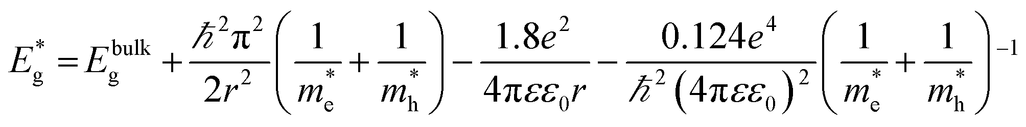 | (1) |
 = band gap energy of CdS QDs determined from the UV-Visible absorbance spectrum and calculated as ℏc/λc, where λc is the cut-off wavelength and c is the speed of light, Ebulkg = band gap energy of the bulk CdS at room temperature, which has the value of 3.88 × 10⁻¹⁹ J, ℏ = Planck's constant, 6.625 × 10⁻³⁴ J s, r = particle radius (m), me = mass of a free electron, 9.11 × 10⁻³¹ kg,
  effective mass of a conduction band electron in CdS,
  effective mass of a valence band hole in CdS, e = elementary charge, 1.602 × 10⁻¹⁹ C, ε0 = permittivity of free space, 8.854 × 10⁻¹² C2 N−1 m−1, ε = 5.7 relative permittivity of CdS.
The surface morphology of the TiO2 NTs before and after deposition of CdS QDs was studied using a Tescan Mira X3 field emission scanning electron microscope (FESEM). The distribution of CdS QDs within the TiO2 nanotubes was analyzed by high resolution TEM (HRTEM) Jeol JEM-2100F and Jeol JEM-2100 operating at 200 kV and the chemical mapping was performed using energy dispersive spectroscopy (EDS) and electron energy loss spectroscopy (EELS). For TEM analysis, the samples were scratched with a diamond needle and the resulting fragments were collected on a grid. The EDS results were provided by analyzing several such obtained fragments. For EELS analysis, the N-doped sample was drowned to epoxy on both sides. Then the etching of the glass substrate was performed with HF until the glass was consumed. The cutting of the remaining film from the opposite side was done using a diamond ultramicrotome knife until the ∼70 nm thin film was obtained and transferred to a carbon grid.
For determination of phase composition of the annealed films, near edge X-ray absorption fine structure (NEXAFS) measurements were performed using synchrotron radiation.
The laboratory X-ray photoelectron spectroscopy (XPS) preliminary analyses (wide scan survey) were performed using 1253.6 eV Mg Kα beam source to check the overall chemical composition of the samples. The high-resolution synchrotron radiation photoelectron spectroscopy (SRPES) enabled the extraction of the N 1s line from the Cd 3d line, expected at 400 eV, in the photoemission spectra of the doped sample with CdS. By varying the incident energy of the beam it was possible to distinguish the valence band position of the reference undoped sample and to compare it with the N-doped sample with and without of CdS. The analyses were performed at the Materials Science Beamline at Elettra synchrotron light source in Trieste.
The diffuse reflectance spectra (DRS) of the undoped and doped TiO2 NTs film formed on FTO glasses and nanocomposites obtained after deposition of CdS QDs were investigated using a Shimadzu 2600 UV-Vis spectrophotometer with an integrating sphere attachment in the wavelength range from 300 to 750 nm. A bare FTO glass was taken as a reference for measuring the baseline.
Results and discussion
A dark field TEM micrograph of the CdS nanoparticles stabilized with MS in Fig. 1(a) exhibits the nanoparticles with the size within the range 2–5 nm. It is a representative image showing that nanoparticles did not agglomerate and that MS was efficient as a surfactant preserving the individuality of the nanoparticles. The absorption spectrum of the colloid is shown in Fig. 1(b) with the absorption edge λc = 462 nm inferred from the intersection of the tangent line and x-axis. The absorption blue shift, with regards to the absorption edge of a bulk CdS (λg = 517 nm), indicates that CdS particles are in the quantum confinement regime.26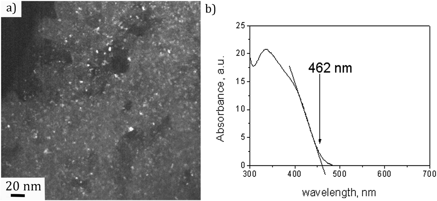 | ||
| Fig. 1 (a) Dark field TEM micrograph and (b) absorption spectrum of the CdS colloid. | ||
Taking into account that the band gap of the CdS QDs,  , is 4.30 × 10⁻¹⁹ J (2.68 eV), the estimated size of CdS QDs was calculated to be 4.5 nm. This value corresponds to the biggest nanoparticle present in the analysed colloid. If we take into account that MS is on the surface of the nanoparticles, it can be said that the EMM approximation was in accordance with TEM observation since the biggest nanoparticle that was detected was 5 nm.
Fig. 2 presents the SEM micrographs of TiO2 NTs after annealing in air and NH3 with a length of ∼2 μm and ∼60 nm inner diameter. It was observed that the open nanotubular structure is preserved both cases. This is important for the subsequent deposition of CdS QDs.
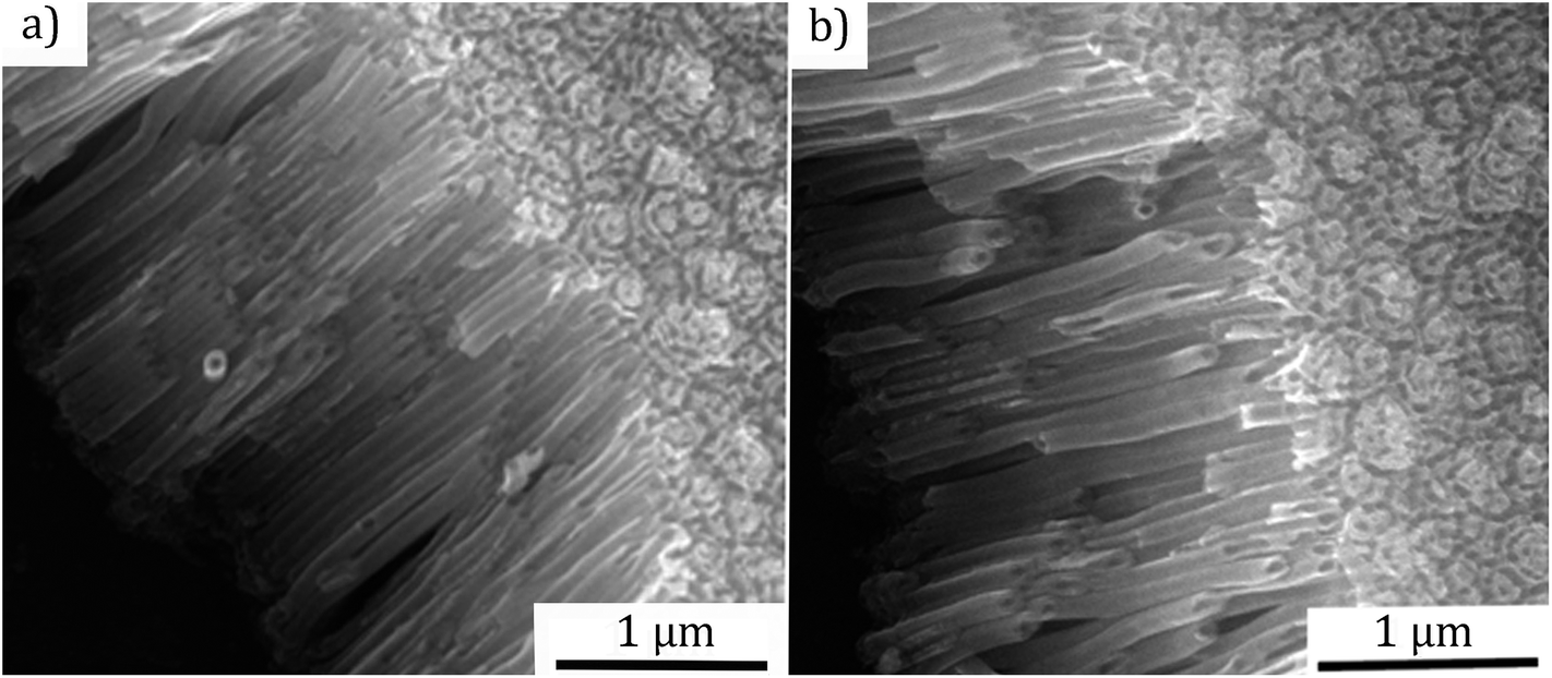 | ||
| Fig. 2 SEM micrographs of the anodized TiO2 nanotubes: (a) after the annealing in air, (b) after the annealing in NH3 (length ∼ 2 μm, inner diameter ∼ 60 nm). | ||
SEM analysis was repeated after 48 hours immersion of TiO2 substrates into CdS colloid. The results are provided in ESI as Fig. S1.† The deposition of CdS QDs was not uniform. There were sporadic areas that cover the nanotubes tops for both undoped and doped TiO2 films. The EDS mapping confirmed that those areas consist more of CdS (Cd:S = 1.07:1.69 at% in average for the undoped sample and 0.57:0.62 at% for the doped sample). However, CdS was also detected within the uncovered film surface (Cd:S = 0.33:0.56 at% in average for the undoped sample and 0.10:0.14 at% for the doped sample). Since S originates both from CdS QDs as well as from MS as a surfactant, it was therefore expected to detect a higher amount of S with regards to Cd (Cd/S relative ratios were all <1). The EDS mapping were recorded from the areas displayed in Fig. S1† and it was used just to confirm the overall presence of Cd and S within the structure. Most of the TiO2 films remain open as they were before deposition without indication of the deposit presence. However, the SEM/EDS characterization gave an insight of the surface composition and morphology only. In order to analyse the structure along the nanotubes depth, the TEM analyses have been performed by using the preparation method described in Experimental part.
The HRTEM micrograph of the undoped TiO2 samples after the 48 h immersion in CdS sol is presented in Fig. 3(a). The nanoparticles are clearly visible within the nanotubular structure and they are ∼5.5 nm in size. It can also be observed that the wall thickness of the nanotube is ∼20 nm. The measured interplanar distance (d = 0.342 nm) of the nanotube's fragment presented in Fig. 3(b) corresponds to (101) plane of the anatase phase of TiO2 (d = 0.352 nm). The 0.010 nm difference could be a consequence of a presence of some other elements in TiO2 structure, for example Sn, as a result of diffusion from FTO support during the annealing in air.
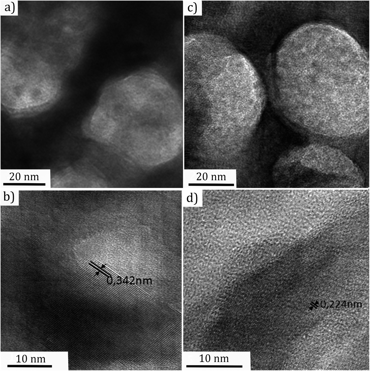 | ||
| Fig. 3 TEM micrographs of: (a) undoped TiO2 NTs with CdS nanoparticles, (b) fragment of the nanotube's wall of the undoped film, (c) doped TiO2 NTs with CdS nanoparticles and (d) fragment of the nanotube's wall of the doped film. | ||
The presence of CdS nanoparticles inside the nanotubular structure of the doped TiO2 film was evident from the micrograph given in Fig. 3(c). The interplanar distance of the nanotube's fragment from Fig. 3(d) is d = 0.224 nm, which is close to the value characteristic for (112) plane of anatase (d = 0.233 nm), but also for the (200) of rutile (d = 0.230 nm). This crystallography difference could be primely due to N incorporation originating from the annealing in NH3. However, it could also be due to the presence of other elements, as noticed for the undoped sample.
By having the advantage of using the synchrotron beamline it was possible to explore the phase composition of TiO2 annealed in ammonia, in relation with the change in crystallography observed in HRTEM. Anatase phase structure of the TiO2 film was evidenced by NEXAFS analysis as depicted in Fig. 4. Ti L2,3 edge presented in Fig. 4(a) and O K edge in Fig. 4(b) were analyzed and compared to literature. For Ti L2,3 edge, the position of six characteristic peaks originating from the splitting of L2 and L3 edges, should be analyzed as explained before.28 However, the differences of the peaks positions between anatase and rutile are negligible in the given spectrum. The distinction could be made only by comparing the intensities of the peaks at 460.5 eV and 461.0 eV. In the case of anatase phase the first one has higher intensity,29–31 as in the spectrum given in Fig. 4(a). The O K edge exhibits two characteristic peaks at 531.4 eV and 534.1 eV, with the separation of 2.7 eV, which matches to the reported value for anatase,28 in contrast to rutile phase that has wider separation (3.0 eV) of the peaks positions. Another observation that confirms the stated phase is the shape of high energy spectrum with two wide shoulders centered at 539.7 eV and 545.6 eV. In the case of amorphous TiO2, there is only one shoulder in this energy range, while in the case of rutile there are three shoulders.28,32
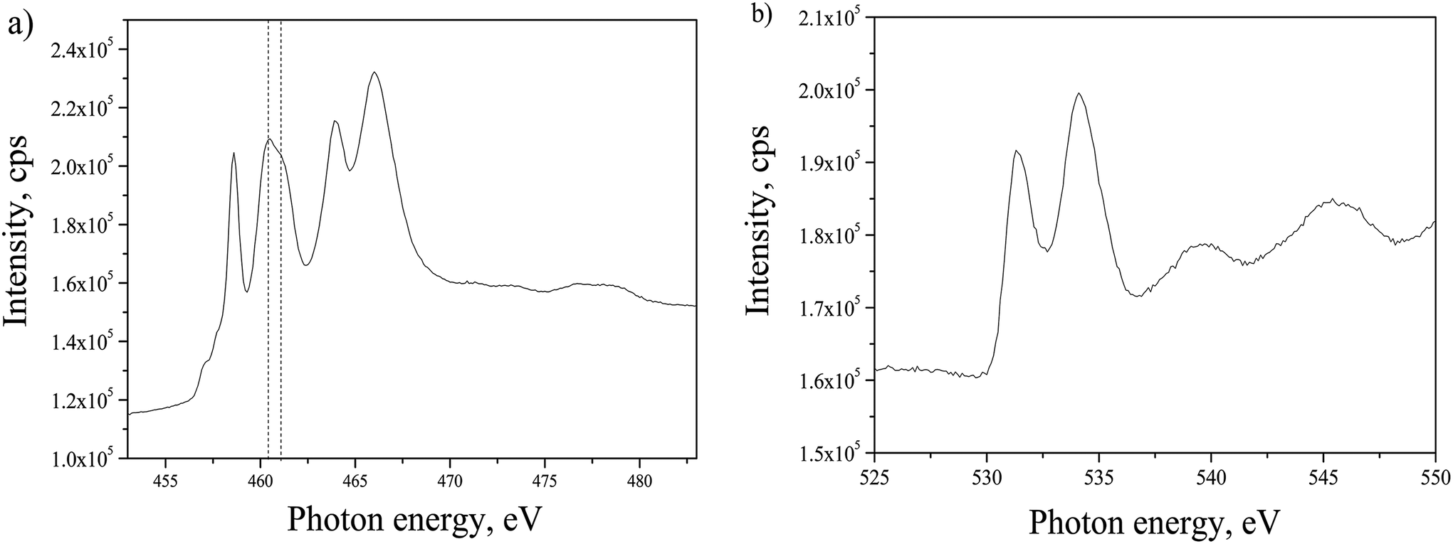 | ||
| Fig. 4 NEXAFS spectra of the doped TiO2 film, representing: (a) Ti L edge and (b) O K edge. | ||
The results of the EDS analyses performed on TEM are summarized in Table 1. Excepting the presence of Ti, O, Cd, S, Si, C and N for the doped sample, there is a significant amount of Sn detected in all analyzed fragments. We advance here the assumption that Sn diffused into TiO2 structure during the annealing,33,34 as it can be the case of Na and Ca35 that are also detected in small amounts. It must be noted that Cu originates from the classical TEM grid used as sample support in the analyses.
| Element | Undoped TiO2/CdS | Doped TiO2/CdS |
|---|---|---|
| C | 52.20 | 60.91 |
| N | 0.00 | 1.89 |
| O | 21.49 | 11.46 |
| Na | 0.18 | 0.60 |
| Si | 1.82 | 3.55 |
| S | 1.55 | 4.24 |
| Ca | 0.08 | 0.00 |
| Ti | 15.97 | 3.72 |
| Cu | 4.67 | 10.77 |
| Cd | 0.67 | 2.16 |
| Sn | 1.33 | 0.72 |
According to the Sn/Ti ratio (0.083 for the undoped TiO2/CdS and 0.194 for the doped TiO2/CdS), the incorporation of Sn in the TiO2 structure was more intensive in doped sample. This is in agreement with the high reactivity of SnO2 to NH3, as reported before.36 Actually, SnO2 acts as a sensor for NH3 even at room temperature.37 Therefore, one may assume that during annealing in NH3 at 450 °C, Sn from FTO diffused more into TiO2 structure than during the annealing in air.
Due to a relatively low sensitivity of the EDS technique for the detection of light elements such as N, additional analyses were performed using EELS, a more appropriate spectroscopy method to analyse the presence of N within the doped sample.
In order to access the NTs structure more distinctly, the preparation of the sample was done by slicing the sample perpendicularly to the substrate to ∼70 nm thin film using a diamond ultramicrotome knife as described in Experimental part. That way only the sensitized NTs could be analyzed in cross section without the possible contribution of the substrate. The STEM micrograph of a representative fragment is shown in Fig. 5(a). The NTs decorated with nanoparticles are clearly visible. The EELS spectrum, associated to the image, is displayed in Fig. 5(b). Herefrom one can observe the Ti L2,3 line doublet at 460 eV and O K line at around 535 eV. A further zoom on the spectrum (inset of Fig. 5(b)) has indicated a weak N K edge at 400 eV suggesting the doping with N. Thus, the studied sample still needed a deeper insight for a sure confirmation of N doping in TiO2 structure. The corresponding XPS analyses were therefore performed.
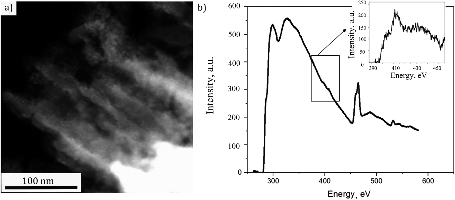 | ||
| Fig. 5 (a) STEM image of the analyzed fragment, (b) energy loss spectrum of the doped TiO2 nanotubes decorated with CdS (a zoom of N K edge is given in the inset). | ||
The wide scan XPS spectra as recorded from the undoped and doped TiO2 films are shown in Fig S2.† The analysis of the spectrum in Fig. S2(a)† confirms the presence of TiO2, as well as of a small amount of Sn by detecting the Sn 3d and Sn 3p3/2 lines at 487 eV and at 717 eV, respectively. The spectrum of the doped sample (Fig. S2(b)†) shows a higher amount of Sn. This confirms the assumption that Sn diffuses more from FTO substrate when TiO2 is annealed in NH3. The main difference between the two spectra is the presence of N 1s line at 400 eV in the case of doped sample, quite expected for the specimen synthesized by annealing in NH3 atmosphere. The amount of N within the doped sample was estimated to be ∼1 at% calculated by quantitative analysis taking into account peak area/photoionization cross sections.
The confirmation of N-doping of the sample annealed in NH3 atmosphere, is provided in Fig. 6, where XPS spectra of the N 1s line before and after ionic sputtering are given. The sputtering was applied to clean the surface contaminants and to analyze the N occurrence deeper in the structure. Before sputtering the N 1s line was fitted to one wide peak at 400.3 eV (Fig. 6(a)). It was revealed that after sputtering N 1s line has three contributions at ∼400.9 eV, ∼399.7 eV and ∼397.4 eV (peak 1, 2 and 3 in Fig. 6(b), respectively). The first one at 400.9 eV can originate from chemisorbed N2 molecules on the surface of the TiO2.38 The second contribution at ∼399.7 eV can be attributed to interstitially incorporated N39 and/or NH3 that might be bound to defect sites or trapped in the subsurface region.40 The third contribution at ∼397.4 eV can be interpreted as nitride, meaning that N is incorporated substitutionally in the structure.40
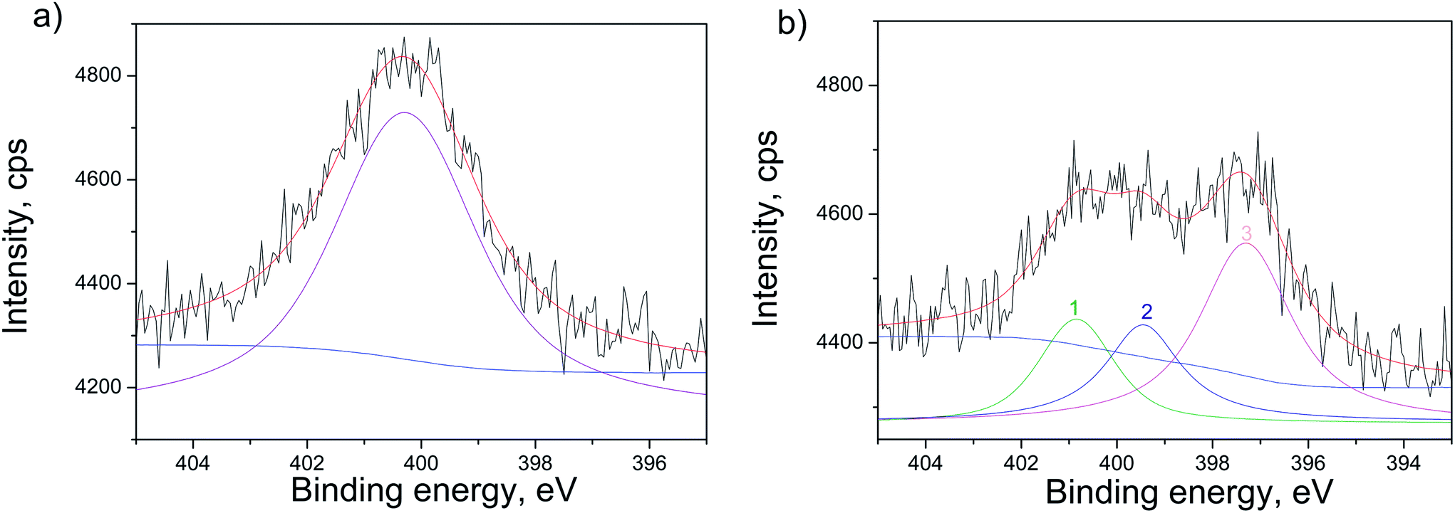 | ||
| Fig. 6 XPS spectra of N 1s line highlighting the different contributions for the N-doped samples with TiO2 film without CdS deposit, measured: (a) before sputtering and (b) after 30 min Ar+ sputtering. The experimental data are given in black, whereas the fitted spectra are in red with the background in blue. The peaks are fitted based on the Gaussian and Lorentzian functions and are presented after the Shirley background subtraction. | ||
The whole range spectra of the undoped and doped samples with CdS are given in Fig. S3.† Apart from the expected lines for Ti, O, Sn and C, one can notice characteristic lines for Cd, S and Si that confirm the presence of CdS with MS on the surface of TiO2. The signal for S originates from both sulfide from CdS core and from MS shell. The signal of C comes from atmospheric CO2, but also it can be attributed to the (–CH2–) groups originating from MS. In addition, there is Si 3p line detected at 99 eV that is assigned to silane groups present in MS around the CdS nanoparticles. In Fig. S3† in the case of CdS/N-doped TiO2 film, an overlapping exists in the ghost peak of Cd 3d line with N 1s line at ∼400 eV.41 That is why only a high-resolution SRPES analysis provided by synchrotron radiation could resolve this issue.
The SRPES investigation was performed on the doped sample with CdS by monitoring N 1s line before and after 10 min of Ar+ sputtering. From Fig. 7 it can be observed that N 1s line has three main contributions and the correspondent intensities changes after sputtering. The first contribution (peak 1 in Fig. 7) at ∼401.5 eV is decreasing, while the ratio of the second contribution at ∼399.9 eV (peak 2) to the third at ∼397.6 eV (peak 3) remained approximately the same after sputtering. This was expected as the first contribution corresponds to chemisorbed N2 molecules on the surface of the TiO2 and they are easily removed by sputtering.38 The second peak at ∼399.9 eV can be attributed to interstitially incorporated N39 and/or NH3 molecules.40 The third contribution at ∼397.6 eV can be associated to N substitutionally incorporated into TiO2 structure.40
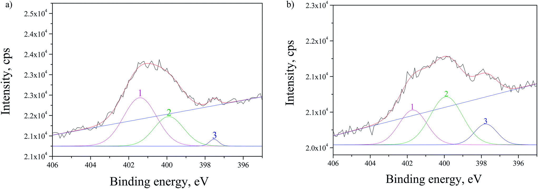 | ||
| Fig. 7 SRPES spectra of N 1s line for N-doped sample with CdS, measured: (a) as received and (b) after 10 min Ar+ sputtering. The experimental data are given in black, whereas the fitted spectra are in red with the background in blue. The peaks are fitted by using the Gaussian and Lorentzian functions. | ||
In order to investigate the effect of the doping and deposition on the narrowing of TiO2 band gap, the incident energy of the synchrotron beam was set at 630 eV for all analyzed samples. This approach allows to clearly distinguish the positions of the valence band maximum (VBM). The overall comparison of the VBM is presented in Fig. 8(a). The VBM positions were estimated to be: 3.95 eV, 3.84 eV, 2.81 eV and 2.91 eV for undoped TiO2, doped TiO2, undoped TiO2 with CdS and doped TiO2 with CdS, respectively. The shift of VBM for the doped TiO2 vs. undoped TiO2 can be a consequence of mixing N 2p and O 2p states and/or introduction of N induced donor level formed within the band gap slightly above O 2p valence zone.42 As demonstrated by the results in Fig. 6 and 7, N was incorporated both interstitially and substitutionally. The CdS/TiO2 films show bigger VBM shifting that can be attributed to CdS deposit.43
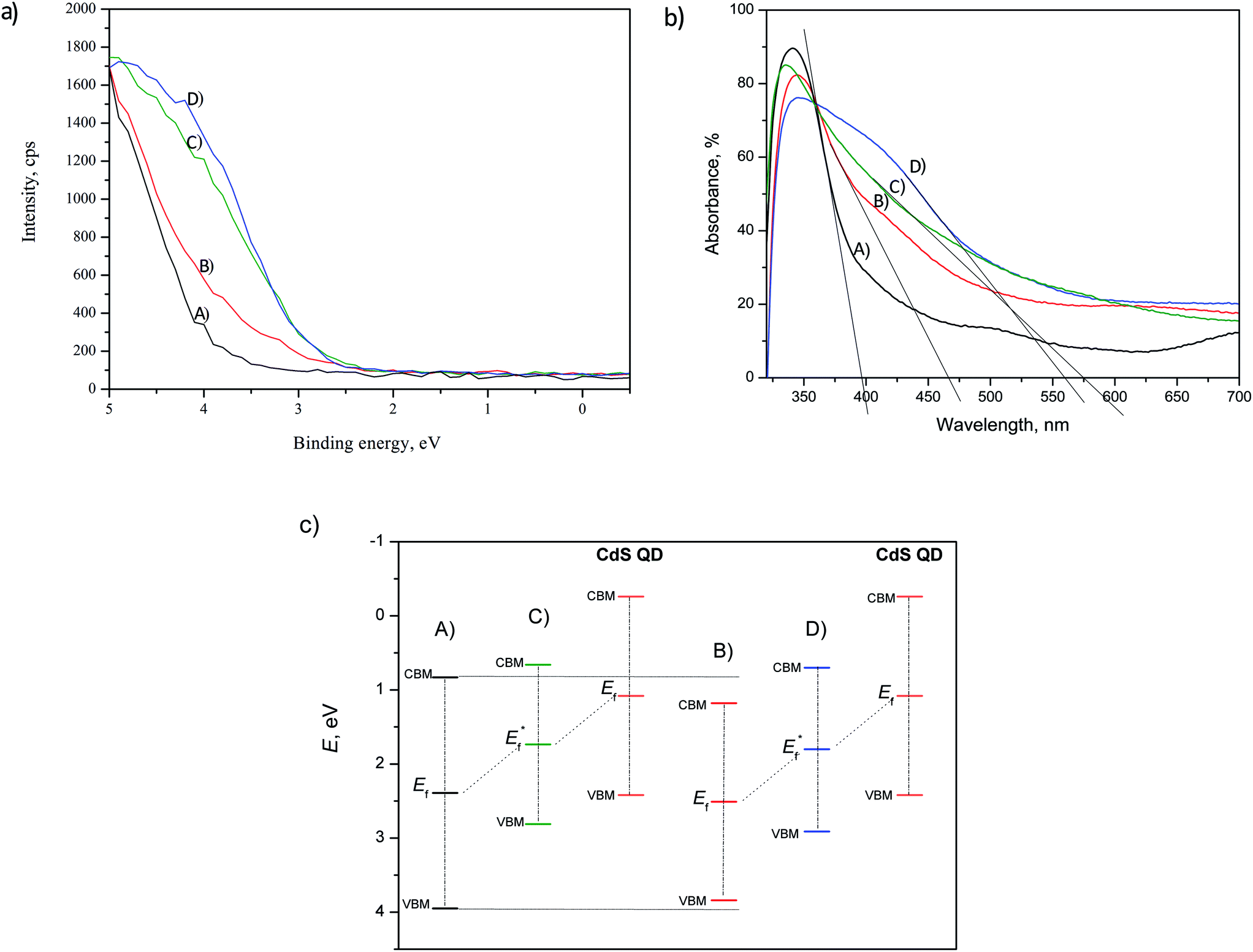 | ||
| Fig. 8 (a) SRPES spectra for determination of the valence band position, (b) absorption spectra with tangent lines for determination of the absorption edges and (c) schematic of the energy levels positions of the: (A) undoped TiO2, (B) doped TiO2, (C) undoped TiO2/CdS and (D) doped TiO2/CdS. | ||
To assess the effect of doping and CdS sensitization on the absorption properties of TiO2 NTs film, the absorption spectra of the bare undoped and doped TiO2 samples were compared with the corresponding spectra of the samples with CdS (Fig. 8(b)). The absorption edges were read at the intersection of the tangent of the absorption curve and the x axis. For the undoped bare TiO2 film, the absorption edge was estimated to be 397 nm, whereas the doped TiO2 film shows an absorption red shift with the edge at 465 nm. The absorption curves of the CdS sensitized TiO2 films proved that the CdS deposition causes the absorption red shift to 575 nm for undoped TiO2/CdS and 560 nm for doped TiO2/CdS films. The smaller red shift of the doped TiO2/CdS as compared to the undoped TiO2/CdS is in agreement with the VBM positions derived from Fig. 8(a). The corresponding band gaps, Eg, of the films were calculated to be: 3.12 eV, 2.66 eV, 2.15 eV and 2.21 eV for undoped TiO2, doped TiO2, undoped TiO2 with CdS and doped TiO2 with CdS, respectively. Taking into account these values, the positions of the conduction band minimum (CBM) were calculated as:44
| CBM = VBM − Eg. | (2) |
The schematic display of energy level positions is given in Fig. 8(c) with the purpose of investigation of the interactions between CdS and TiO2. The Fermi level, Ef, of bare undoped TiO2 is located at 2.39 eV and quasi-Fermi level,  , for the undoped TiO2/CdS composite is at 1.74 eV. Following the alignment of the Fermi levels (difference
 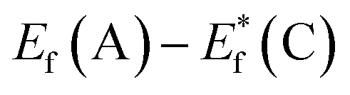 is equal to the difference
 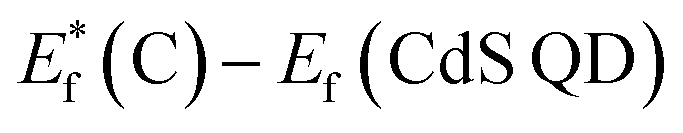 ), we calculated that Ef(CdS QD) is at 1.08 eV. Having in mind that the Eg of CdS is 2.68 eV, the energy level bands for CdS were 2.42 eV and −0.26 eV, for VBM and CBM respectively. When analyzing the energy level positions of the doped system in the same manner as for the undoped the results lead to the same values for CdS QD energy levels positions. This means that the interaction of CdS and TiO2 remains the same irrespective of the doping. This could be due to the MS presence on the surface of CdS QDs.
Another observation is that the band gap of undoped TiO2 is narrower (3.12 eV) comparing to the value characteristic for anatase (3.2 eV4). We believe it is due to Sn incorporation from FTO substrate as suggested in TEM analysis since there is a 0.01 nm difference in interplanar distance that was measured and that of anatase phase. Also, in the case of the doped sample the CBM is moved compared to the undoped one. That can also be due to the loading of Sn from the support. The annealing in NH3 enhanced the diffusion of Sn and it is assumed that Sn acted as cation dopant creating a donor level in the energy gap of TiO2 resulting in additional narrowing of the band gap.44 This assumption has being further studied in our group.
Conclusions
We have investigated the effect of N doping of TiO2 nanotubes (∼2 μm long and ∼60 nm wide) obtained by anodization of titanium film sputtered on FTO glass. The N-doping was reached by annealing the amorphous titania in ammonia atmosphere at 450 °C and it did not affect the nanotubular morphology. The additional enhancement of absorption properties was provided by deposition of CdS quantum dots (2–5 nm sized), that were synthesized using mercaptosilane as a surfactant and binding reagent to TiO2 surface. The deposition was done by immersing the titania substrates into the CdS sol for 48 h. The SEM/EDS analyses showed that the deposition was not well uniform but nanotubular structure remains open. TEM analyses allowed one to gather a clear insight on the nanocomposites structure. It showed that CdS nanoparticles were deposited inside the nanotubes but also that the doped nanotubes had a smaller interplanar distance as compared to the undoped ones, whose interplanar distance corresponded to anatase phase. This difference was attributed to N doping and Sn migration from the substrate. The presence of Sn and N in the doped sample was confirmed by EDS combined with EELS analysis. Owing to high resolution synchrotron radiation, the NEXAFS analysis proved that also the doped TiO2 film had anatase phase. Details on the surface chemical composition of the studied samples were provided by XPS. By analyzing the N 1s line it was shown that N was incorporated both interstitially and substitutionally in TiO2 lattice, with a decreased contribution of the interstitial after ionic sputtering. The shift of the VBM position for doped TiO2 vs. undoped TiO2 proved the narrowing of the band gap. The CdS/TiO2 films exhibit bigger VBM shifting that can be attributed to CdS deposit. By measuring the absorption spectra of the bare undoped and doped TiO2 samples, it was shown that doping caused the red shift from 397 to 465 nm. Furthermore the CdS deposition additionally enhanced the absorption in the visible range (575 nm for undoped TiO2/CdS and 560 nm for doped TiO2/CdS films).Conflicts of interest
There are no conflicts to declare.Acknowledgements
The Serbian authors acknowledge with thanks the financial support of the Ministry of Education, Science and Technological Development, Republic of Serbia through the Project III 45019. The XPS analyses done at Elettra synchrotron in Trieste as well as at Charles University in Prague were accomplished thanks to the financial support of the CERIC-ERIC Consortium (20152050 proposal) and of the Czech Ministry of Education (grant LM2015057), whereas the French Institute in Belgrade supported the research done in IPCMS. A. Bjelajac is grateful to Dris Ihiawakrim from IPCMS for enabling the sample preparation for TEM analyses. The Romanian authors acknowledge with thanks the partial financial support of this work in the frame of the contract POC-G 135/23.09.2016. M. Vondraček was supported by the Czech Ministry of Education, Youth and Sports (grant LG15050).Notes and references
- H. Zhang, X. Lv, Y. Li, Y. Wang and J. Li, ACS Nano, 2010, 4, 380 CrossRef CAS PubMed.
- P. Roy, D. Kim, I. Paramasivam and P. Schmuki, Electrochem. Commun., 2009, 11, 1001 CrossRef CAS.
- H. Wang, et al., Phys. Chem. Chem. Phys., 2011, 13, 7008 RSC.
- D. A. H. Hanaor and C. C. Sorrell, J. Mater. Sci., 2011, 46, 855 CrossRef CAS.
- T. López-Luke, et al., J. Phys. Chem. C, 2008, 112, 1282 CrossRef.
- P. Roy, S. Berger and P. Schmuki, Angew. Chem., Int. Ed., 2011, 50, 2904 CrossRef CAS PubMed.
- D. R. Baker and P. V. Kamat, Adv. Funct. Mater., 2009, 19, 805 CrossRef CAS.
- G. K. Mor, K. Shankar, M. Paulose, O. K. Varghese and C. A. Grimes, Nano Lett., 2006, 6, 215 CrossRef CAS PubMed.
- S. Meng, J. Ren and E. Kaxiras, Nano Lett., 2008, 8, 3266 CrossRef CAS PubMed.
- G. L. Mor and C. A. Grimes, TiO2 Nanotube Arrays Synthesis, Properties, and Applications, Springer, Berlin, Heidelberg, 2009 Search PubMed.
- H. Wu and Z. Zhang, Int. J. Hydrogen Energy, 2011, 36, 13481 CrossRef CAS.
- R. P. Vitiello, J. M. Macak, A. Ghicov, H. Tsuchiya, L. F. P. Dick and P. Schmuki, Electrochem. Commun., 2006, 8, 544 CrossRef CAS.
- D. Kim, S. Fujimoto, P. Schmuk and H. Tsuchiya, Electrochem. Commun., 2008, 10, 910 CrossRef CAS.
- A. Ghicov, J. M. Macak, H. Tsuchiya, J. Kunze, V. Haeublein, L. Frey and P. Schmuki, Nano Lett., 2006, 6, 1080 CrossRef CAS.
- R. P. Antony, T. Mathews, P. K. Ajikumar, D. N. Krishna, S. Dash and A. K. Tyagi, Mater. Res. Bull., 2012, 47, 4491 CrossRef CAS.
- K. Shankar, K. C. Tep, G. K. Mor and C. A. Grimes, J. Phys. D: Appl. Phys., 2006, 39, 2361 CrossRef CAS.
- M. Grätzel and B. O'Regan, Nature, 1991, 353, 737 CrossRef.
- Y. L. Lee and Y. S. Lo, Adv. Funct. Mater., 2009, 19, 604 CrossRef.
- M. A. A. Schoonen and Y. Xu, Am. Mineral., 2000, 85, 543 CrossRef.
- H. Wang, Y. Bai, H. Zhang, Z. Zhang, J. Li and L. Guo, Chem. Phys. Lett., 2011, 508, 130 CrossRef.
- A. Bjelajac, R. Petrović, J. M. Nedeljković, V. Djokić, T. Radetić, J. Ćirković and Dj. Janaćković, Ceram. Int., 2015, 41, 7048 CrossRef CAS.
- G. K. Mor, O. K. Varghese, M. Paulose, K. G. Ong and C. A. Grimes, Thin Solid Films, 2006, 496, 42 CrossRef CAS.
- D. Chen, Y. Gao, G. Wang, H. Zhang, W. Lu and J. Li, J. Phys. Chem. C, 2007, 111, 13163 CrossRef CAS.
- A. Ghicov, H. Tsuchiya, J. M. Macak and P. Schmuki, Electrochem. Commun., 2005, 7, 505 CrossRef CAS.
- A. Bjelajac, V. Djokić, R. Petrović, N. Bundaleski, G. Socol, I. N. Mihailescu, Z. Rakočević and D. Janaćković, Ceram. Int., 2017, 43, 15040 CrossRef CAS.
- L. E. Brus, J. Chem. Phys., 1983, 79, 5566 CrossRef CAS.
- L. E. Brus, J. Chem. Phys., 1984, 80, 4403 CrossRef CAS.
- S. Kucheyev, T. van Buuren, T. Baumann, J. Satcher, T. Willey, R. Meulenberg, T. Felter, J. Poco, S. Gammon and L. Terminello, Phys. Rev. B: Condens. Matter Mater. Phys., 2004, 69, 1 CrossRef.
- M. Bagge-Hansen, A. Wichmann, A. Wittstock, J. R. I. Lee, J. Ye, T. M. Willey, J. D. Kuntz, T. Van Buuren, J. Biener, M. Ba and M. M. Biener, J. Phys. Chem. C, 2014, 118, 4078 CrossRef CAS.
- R. Ruus, A. Kikas, A. Saar, A. Ausmees, E. Nõmmiste, J. Aarik, A. Aidla, T. Uustare and I. Martinson, Solid State Commun., 1997, 104, 199 CrossRef CAS.
- H. A. Hamedani, N. K. Allam, M. A. El-Sayed, M. A. Khaleel, H. Garmestani and F. M. Alamgir, Adv. Funct. Mater., 2014, 24, 6783 CrossRef CAS.
- T. C. Kaspar, A. Ney, A. N. Mangham, S. M. Heald, Y. Joly, V. Ney, F. Wilhelm, A. Rogalev, F. Yakou and S. A. Chambers, Phys. Rev. B: Condens. Matter Mater. Phys., 2012, 86, 35322 CrossRef.
- R. G. Palgrave, A. Bourlange, D. J. Payne, J. S. Foord and R. G. Egdell, Cryst. Growth Des., 2009, 9, 1793 CrossRef CAS.
- A. V. Virkar and H. P. Naidu, J. Am. Ceram. Soc., 1998, 81, 2176 Search PubMed.
- J. M. Herrmann, H. Tahiri, C. Guillard and P. Pichat, Catal. Today, 1999, 54, 131 CrossRef CAS.
- F. Shao, F. Hernandez-Ramirez, J. D. Prades, J. R. Morante and N. Lopez, Procedia Eng., 2012, 47, 293 CrossRef CAS.
- N. Van Hieu, L. T. B. Thuy and N. D. Chien, Sens. Actuators, B, 2008, 129, 888 CrossRef CAS.
- S. H. Kang, H. S. Kim, J. Y. Kim and Y. E. Sung, Mater. Chem. Phys., 2010, 124, 422 CrossRef CAS.
- J. Geng, D. Yang, J. Zhu, D. Chen and Z. Jiang, Mater. Res. Bull., 2009, 44, 146 CrossRef CAS.
- I. Takahashi, D. J. Payne, R. G. Palgrave and R. G. Egdell, Chem. Phys. Lett., 2008, 454, 314 CrossRef CAS.
- M. O. Krause and J. G. Ferreira, J. Phys. B: At. Mol. Phys., 1975, 8, 2007 CrossRef CAS.
- R. Asahi, T. Morikawa, T. Ohwaki, K. Aoki and Y. Taga, Science, 2001, 293, 269 CrossRef CAS PubMed.
- V. Etacheri, M. K. Seery, S. J. Hinder and S. C. Pillai, Adv. Funct. Mater., 2011, 21, 3744 CrossRef CAS.
- G. Pan, W. Jing, L. Qing-Ju and Z. Wen-Fang, Chin. Phys. B, 2010, 19, 087103 CrossRef.
Footnote |
| † Electronic supplementary information (ESI) available. See DOI: 10.1039/c8ra06341a |
| This journal is © The Royal Society of Chemistry 2018 |