
 Open Access Article
 This Open Access Article is licensed under a Creative Commons Attribution-Non Commercial 3.0 Unported Licence
Resistive switching of the HfOx/HfO2 bilayer heterostructure and its transmission characteristics as a synapse
Tingting Tan *,
Yihang Du,
Ai Cao,
Yaling Sun,
Hua Zhang and
Gangqiang Zha*
*,
Yihang Du,
Ai Cao,
Yaling Sun,
Hua Zhang and
Gangqiang Zha*
State Key Laboratory of Solidification Processing, MIIT Key Laboratory of Radiation Detection Materials and Devices, School of Materials Science and Engineering, Northwestern Polytechnical University, Xi'an 710072, China. E-mail: tantt@nwpu.edu.cn; zha_gq@nwpu.edu.cn
First published on 14th December 2018
Abstract
In this work, HfOx/HfO2 homo-bilayer structure based resistive random access memory devices were fabricated, and the resistive switching characteristics of the devices were investigated. The samples with an Ar/O2 ratio of 12![[thin space (1/6-em)]](https://www.rsc.org/images/entities/char_2009.gif) :2 exhibited improved switching performance including better uniformity, endurance and retention, which was selected to imitate the “learning” and “forgetting” function of biological synapses. The multilevel conductance of the HfOx/HfO2 homo-bilayer structure under the model of pulse voltage suggests its potential to emulate the nonlinear transmission characteristics of the synapse, and a model of multilevel conductance of the HfOx/HfO2 homo-bilayer structure was proposed. The device conductance continuously increases (decreases) in accordance with the number of positive (negative) voltage pulses during the potentiation (depression) process, which can emulate the change of synaptic weight in a biological synapse.
:2 exhibited improved switching performance including better uniformity, endurance and retention, which was selected to imitate the “learning” and “forgetting” function of biological synapses. The multilevel conductance of the HfOx/HfO2 homo-bilayer structure under the model of pulse voltage suggests its potential to emulate the nonlinear transmission characteristics of the synapse, and a model of multilevel conductance of the HfOx/HfO2 homo-bilayer structure was proposed. The device conductance continuously increases (decreases) in accordance with the number of positive (negative) voltage pulses during the potentiation (depression) process, which can emulate the change of synaptic weight in a biological synapse.
Introduction
Nanoscale transition metal oxide-based resistive switching random access memory (RRAM) devices, due to their various virtues, including high operating speed, low power consumption and excellent scalability, have attracted a great deal of attention.1–4 In recent years, a lot of effort has been focused on RRAM based on a bilayer heterostructure consisting of two different oxides or the same oxide with different oxygen contents in virtue of its peculiar performance, such as multilevel resistive switching,5–7 self-rectification functionalities,8–11 and synaptic emulation.12 RRAM has been proposed to emulate the synapse owing to their similarity with nonlinear transmission characteristics. The synapse is an essential two-terminal device, including the pre-neuron and post-neuron synapse, which is remarkably similar to the metal–insulator–metal structure of the resistive switching devices.13,14 In biological systems, the connection intensity between the presynaptic neuron and the postsynaptic neuron is called synaptic weight, which can be regulated by ionic flow through them and it is generally recognized that the change of synaptic weight enables biological systems to learn and function.15,16 Analogous to the biological synapse, the conductance of the resistive switching devices can be viewed as the biological synaptic weight, and the conductance can be modified by precisely regulating the input pulses and via regulating the charge flow through the device.13 There are some different materials used for fabricating and designing memristors (memory + resistor), such as TiO2,15 Ag2S,17 PEDOT:PSS18 and InGaZnO.19 Memristors were used to emulate the nonlinear transmission characteristics of the synapse.In this paper, the HfOx/HfO2 homo-bilayer structure based RRAM devices have been fabricated, and the switching layer of the devices consists of two parts: the conducting layer (oxygen-deficient ∼ HfOx) and the insulating layer (oxygen-rich ∼ HfO2). For the oxygen-deficient layer, the chemical composition of the HfOx films with different concentration of oxygen was investigated, in which the oxygen content in HfOx film was modified by changing the Ar/O2 ratios during the deposition process. Subsequently, the resistive switching characteristics of the HfOx/HfO2 bilayer heterostructure were investigated. The uniformity of RS parameters and the reliability of the samples were analyzed. Finally, the device based on the HfOx/HfO2 bilayer structure was used to emulate the nonlinear transmission characteristics of the synapse.
Experimental
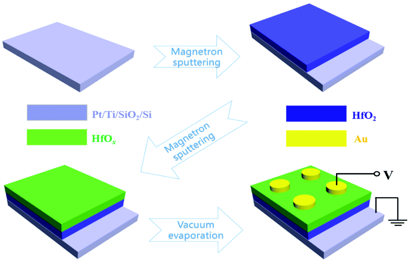
In this experiment, the schematics diagram of fabrication process for the HfOx/HfO2 homo-bilayer structure is shown in Fig. 1, the Si/SiO2/Ti/Pt substrates were used as continuous bottom electrode, and then 15 nm-thick stoichiometric HfO2 films were deposited on pre-cleaned Pt substrates by radio frequency (RF) magnetron sputtering at room temperature (RT). Afterwards, the ∼15 nm-thick oxygen-deficient HfOx films were grown on HfO2 films by RF reactive magnetron sputtering at RT in a gaseous mixture under different Ar/O2 ratios, which was 12:1 (“Device 1”), 12:2 (“Device 2”) and 12:3 (“Device 3”) respectively. The RF power of 70 W and the working pressure of 0.3 Pa were utilized. Finally, the Au top electrodes with a diameter of 2 mm were deposited by thermal evaporation using a shadow mask. The thicknesses of HfOx and HfO2 films were measured by the spectroscopic ellipsometer. The chemical bonding states and chemical composition of HfOx films in the HfOx/HfO2 heterostructure was examined via X-ray photoelectron spectroscopy (XPS). The conventional electrical properties were tested using an Agilent B1500 semiconductor parameter analyzer in voltage sweep mode. During the measurement, the bias voltage was applied to the Au top electrode while the Pt bottom electrode was always grounded, as shown in Fig. 1.
 | ||
| Fig. 1 Schematic diagram of fabrication process for the HfOx/HfO2 bilayer structure. | ||
Results and discussion
The chemical bonding states of the HfOx film in the homo-bilayer structure were investigated by XPS. Fig. 2 shows the Hf 4f and the O 1s spectra in oxygen-deficient HfOx films of the HfOx/HfO2 homo-bilayer structure, which were deposited under different Ar/O2 ratios. The Au top electrodes were not deposited for XPS analysis, the binding energy (Eb) was calibrated with the C–C binding energy of the adventitious C signal (284.6 eV). Fig. 2(a) presents the core level spectra of Hf 4f in the HfOx layer of the homo-bilayer with different Ar/O2 ratios. The position of Hf 4f spectra shift slightly to lower Eb as the O2 flow rate increase, which correspond to Hf–O binds. The result suggests that the concentration of oxygen vacancy (VO) decrease as the O2 flow rate increases, since the Eb of fully oxidized metal oxide is lower than that of oxygen deficient oxide.20 Fig. 2(b) shows the O 1s spectra of the HfOx layer in the homo-bilayer structure, the position of O 1s peak also shifted towards lower Eb direction, which corroborates the Hf 4f spectra. By calculating the area proportion of each peak, the atomic ratio of O/Hf in the HfOx film were 1.64, 1.81, 1.92 respectively.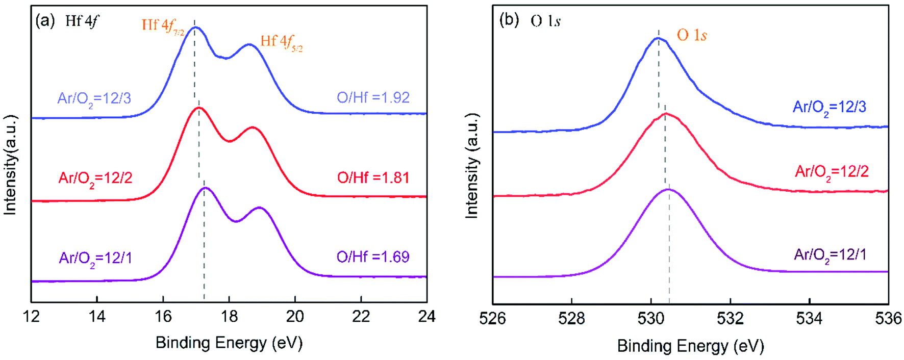 | ||
| Fig. 2 The XPS spectra of (a) Hf 4f and (b) O 1s of the HfOx films deposited under different Ar/O2 ratios in the HfOx/HfO2 bilayer structure. | ||
The electroforming process and subsequent resistive switching (RS) current–voltage (I–V) curves of the HfOx/HfO2 bilayer structure are plotted in Fig. 3. For the RRAM device, the large forming voltage (Vf) is needed to form the localized conductive filament (CF) before the electrical measurements.21 The forming process creates localized conducting paths whose formation/rupture plays a crucial role in the subsequent RS characteristics. Fig. 3(a) shows the Vf of different devices at RT, the Vf increases as the O2 flow rate increased, which can be attributed to the reduction of oxygen vacancies concentration.4,22,23 Fig. 3(b–d) depict the typical I–V curves of the different samples measured for 50 cycles. All the devices present bipolar resistive switching (BRS), i.e. it switches from high resistance state (HRS) to low resistance state (LRS) when positive voltage was applied and returned to HRS during negative voltage sweeping. A compliance current (Icc) of 1 mA was applied on the samples to avoid hard breakdown and to improve the RS performance.24 It is well known that the formation/rupture of VO CF is widely recognized as the switching mechanism in the transition metal oxides.4,25 Compared with Device 1 and Device 3, Device 2 exhibited good reproducibility, which may be correlated with the appropriate oxygen vacancy concentration in the HfOx layer.
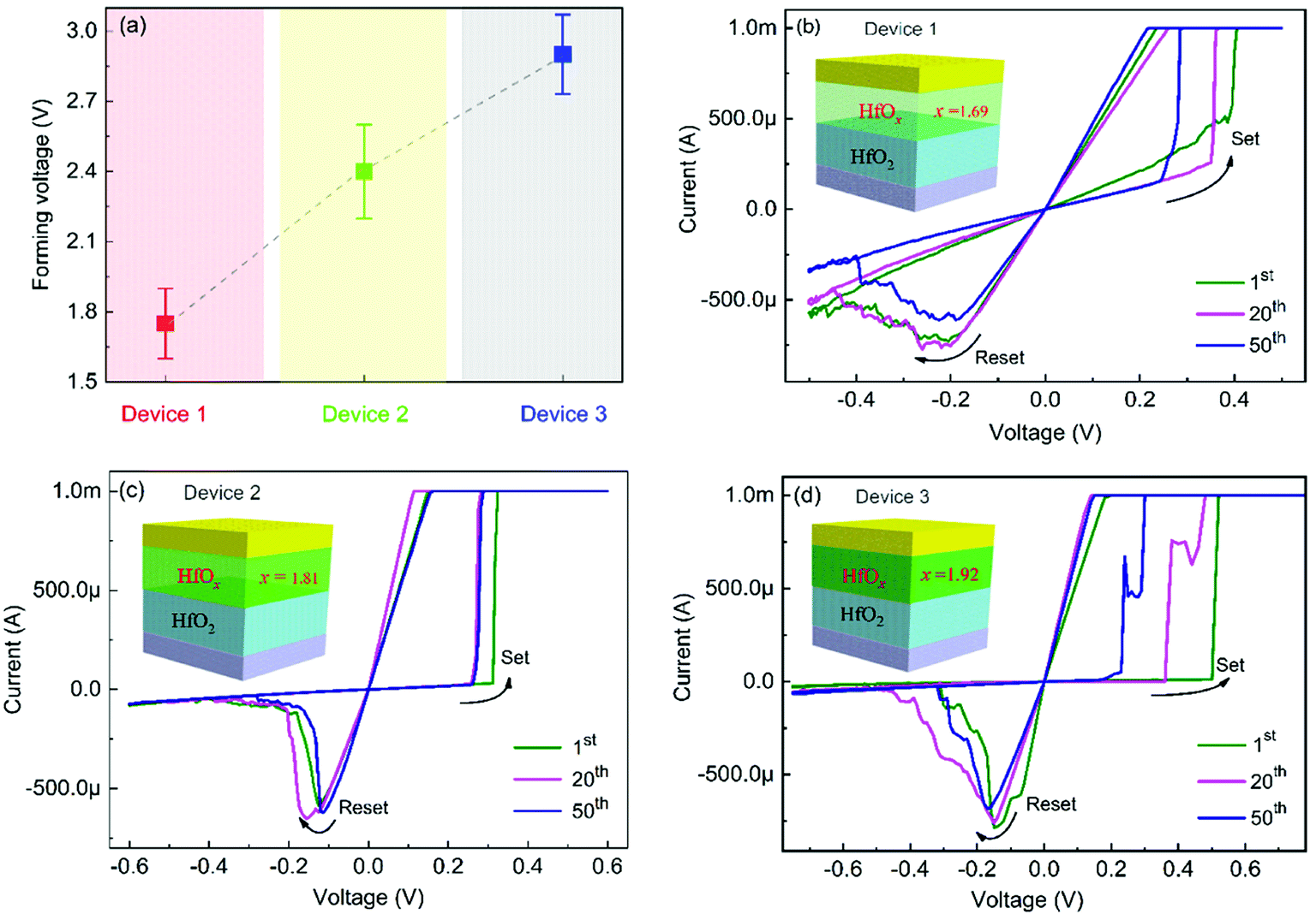 | ||
| Fig. 3 (a) The forming voltage of Device 1, Device 2 and Device 3. The typical bipolar resistive switching characteristics of (b) Device 1, (c) Device 2 and (d) Device 3. The inset of (b–d) show the schematic diagram for Au/HfOx/HfO2/Pt. | ||
Uniformity of RS parameters is very important for the memory application. Fig. 4 plots the statistical results of the distribution of the switching voltage and the resistance of three devices. Fig. 4(a) shows the statistical distribution of set voltage (VSet) and reset voltage (VReset) for different devices. Device 2 exhibits smaller VSet (average value) with relative localized distribution compared with other device (especially Device 3), this may be related to VO concentration in the oxygen-deficient HfOx layer. As can be seen, Device 3 presents higher and decentralized VSet, which may due to the number of RS layer in the Device 3. XPS results revealed that the O/Hf ratio of the HfOx film in the bilayer is 1.92, which indicates the size of CF in HfOx and HfO2 layer is similar. Namely, the resistance of the HfOx layer is close to that of the HfO2 layer. As a matter of fact, the RS occurs in the HfOx layer and the HfO2 layer simultaneously, which increases the complexity of RS process. Consequently, the VSet is relatively high and scattered. In addition, the distribution of the VSet shows more dispersed than that of the VReset. It has been reported that the formation of the CFs in the set process was more random than the rupture of the CFs in the reset process due to the formation process is determined by the competition among different filamentary paths.26 The variation of resistance in HRS (RHRS) and LRS (RLRS) are shown in Fig. 4(b). The RLRS and RHRS enhance with the increasing O2/Ar ratios, which is owing to the augment of insulator conductivity.
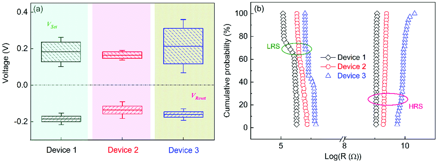 | ||
| Fig. 4 The statistical results of distribution of (a) the switching voltage and (b) the resistance for Device 1, Device 2 and Device 3. | ||
In principle, reliability is an important index to evaluate the function of memory in application. In order to investigate the reliability of the devices, the endurance and the retention properties were presented in Fig. 5. The endurance characteristics of the devices were performed under DC voltage sweeping mode, and the reading voltage was 0.1 V, as presented in Fig. 5(a). The RHRS and RLRS of the HfOx/HfO2 samples show no significant failure after 50 consecutive RS cycles. The retention stability of the HfOx/HfO2 sample was measured with a readout voltage of 0.1 V, as presented in Fig. 5(b). The current of Device 1 in the HRS had evident changes after cumulative waiting time of 104 s. In contrast, the currents of the Device 2 and Device 3 were relatively stable and can maintain 104 s without degradation. The higher VO concentration would lead to the unstabilized oxygen exchange layer.27 With regard to Device 1, the number of VO in the oxygen-deficient HfOx layer is too high. The VO would diffuse from the oxygen-deficient HfOx region to the HfO2 layer under the low electric stress,28 and repair the ruptured filaments or form other connected path due to the VO concentration gradient29 at HRS with the increasing retention time, hence the current of high resistance state increases at 8000 seconds. The moderate VO concentration gradient is a key factor for maintaining sufficient retention, hence the Device 2 exhibited the good retention characteristics, which may be due to the appropriate concentration of VO in the oxygen-defect HfOx layer.
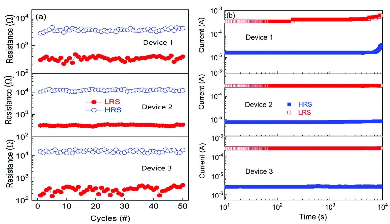 | ||
| Fig. 5 (a) The endurance and (b) the retention characteristics of the Device 1, Device 2 and Device 3. | ||
In the light of above results, the Device 2 presents favorable RS behaviors and gradual reset process, thus it has potential to emulate the nonlinear transmission characteristics of the synapse. Fig. 6 shows the nonlinear transmission characteristics of the Device 2. The potentiation of four cycles is presented in Fig. 6(a), the applied positive DC sweeping voltage ranges from 0 to 0.18 V, which is lower than the VSet to avoid the abrupt set process. For the synaptic response, the gradually enhancing of current level after each sweep suggests that the gradual growth of the filament,30 which can imitate the “learning” process in the biological synapse. The depression of four cycles is presented in Fig. 6(b), the applied negative DC voltage sweeps range from 0 to −0.10 V. The damping current level after each sweep indicates that the oxygen ions can be recombined with the vacancies during the gradual reset process, which can imitate the “forgetting” process. There is no fluctuation or an abrupt change in I–V curves during the sweeping process, which implies the continuous distribution of resistance states could be realized by applying suitable sweeping voltage. In the set and reset process, the conductance of the device can be viewed as the potentiation and the depression in biological synapses, respectively. The conductance continuously increases with the increasing number of positive voltage sweep, and then the device shows the potentiation of the synapses. While the conductance continuously decreases with the increasing number of negative voltage sweep, and then the device shows the inhibition of the synapses. The above phenomena present a close similarity to the nonlinear transmission characteristics of the biological synapses.
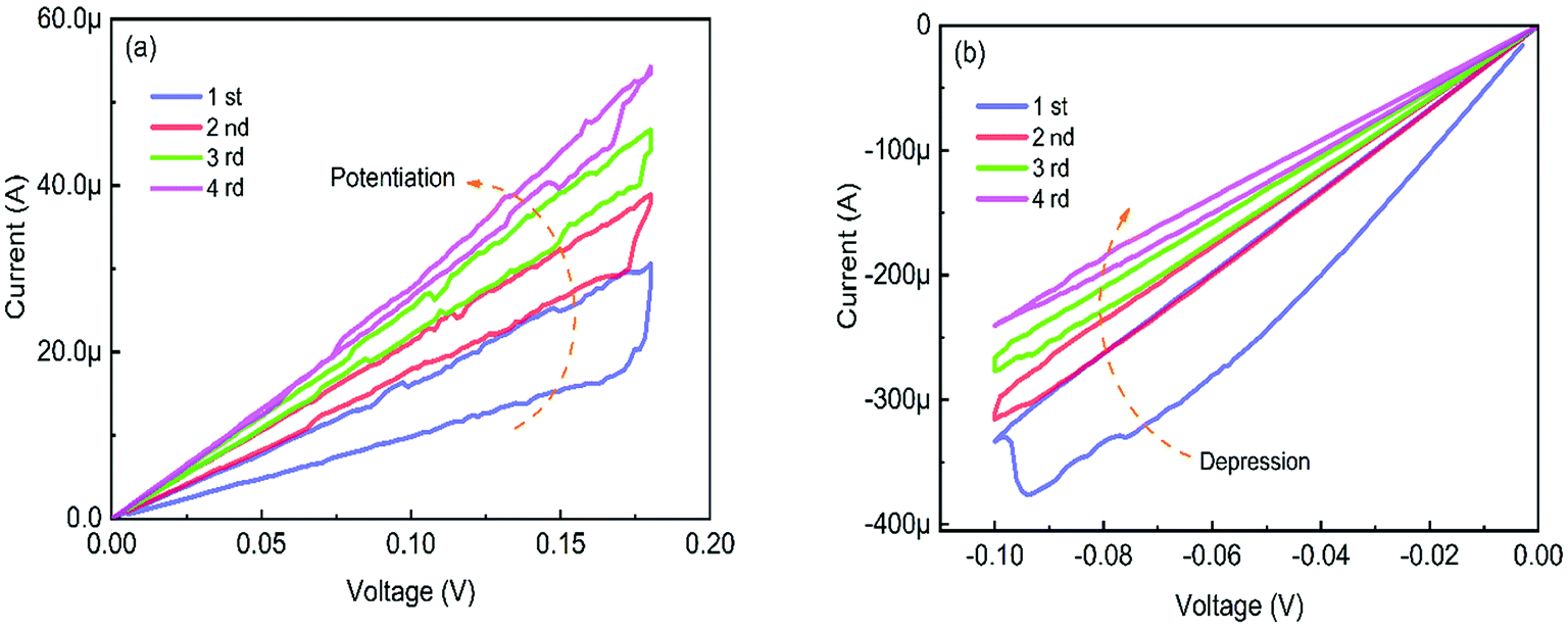 | ||
| Fig. 6 The nonlinear transmission characteristics of the HfOx/HfO2 RRAM. (a) Potentiation behaviors of the Device 2 under positive DC voltage. (b) Depression behaviors of the Device 2 under negative DC voltage. | ||
According to the previous studies, the pulse programming is a more effective method for the practical application due to its high energy efficiency and high operational speed.31 The multiple resistance levels of the Device 2 under the sequential applications of 50 identical positive and negative pulses are shown in Fig. 7(a) and (b), respectively. The resistance changes monotonously along with the voltage pulses, which is related to the charge flowing through the device.32 The current of the device continuously increases (decreases) in accordance with the number of positive (negative) voltage pulses during the potentiation (depression) process, which is in agreement with the results of the DC voltage sweep. If the conductance of the device is viewed as the synaptic weight, the phenomena show a close similarity to the transmission characteristics of biological.
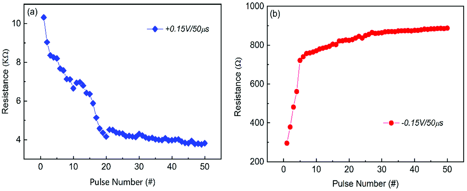 | ||
| Fig. 7 The resistance of Device 2 vs. biasing pulse number: (a) set and (b) reset process. | ||
Multilevel ability is one of the key characteristics for the synaptic application.33,34 Some studies have suggested that partial formation/rupture of filaments in the bilayer RRAM devices.35,36 According to the percolation theory,37 the gradual resistance change under the different number of pulses is due to the generation of oxygen vacancy. On the basis of previous investigation, the formation and rupture of the CFs probably take place at the Pt/HfO2 interface for the bilayer HfOx/HfO2 structures.38,39 Fig. 8 illustrates the multiple resistance levels of Device 2 during the sequential application of identical pulses. Before initiating the resistive switching, an electrical forming process is needed to activate the fresh memory cell into a high conductive state, as shown in Fig. 8(a). During the subsequent reset process, the CFs near the cathode (Pt) are ruptured and forming a tunneling gap region, as illustrated in Fig. 8(b). It is noteworthy that the pulse voltage is lower than the set voltage, and then the CFs are not fully formed. When applying the positive pulse voltage on the Au top electrode, the oxygen anions (O2−) with negative charges are repelled from the HfO2 layer to oxygen-defect HfOx layer, which reserved in the HfOx layer during the positive polarity. The resistance of tunneling gap decreases with the VO accumulated the filament tip40 under sequential application of 50 identical positive pulses, as presented in Fig. 8(c). Hence, the equivalent resistance of the bilayer HfOx/HfO2 heterostructure is reduced, which corresponds to the long-term potentiation (LTP) of the Device 2. Applying the negative pulses on the Au top electrode immediately, the oxygen ions migrate from the oxygen-defect HfOx layer (oxygen reservoir) to the Pt bottom electrode and recombined with the VO accumulated the filament tip under sequential application of 50 identical negative pulses, resulting in the narrowed tunneling gap,41 as shown in Fig. 8(d). Therefore, the equivalent resistance of the bilayer HfOx/HfO2 heterostructure is increased, which corresponds to the long-term depression (LTD) of the Device 2.
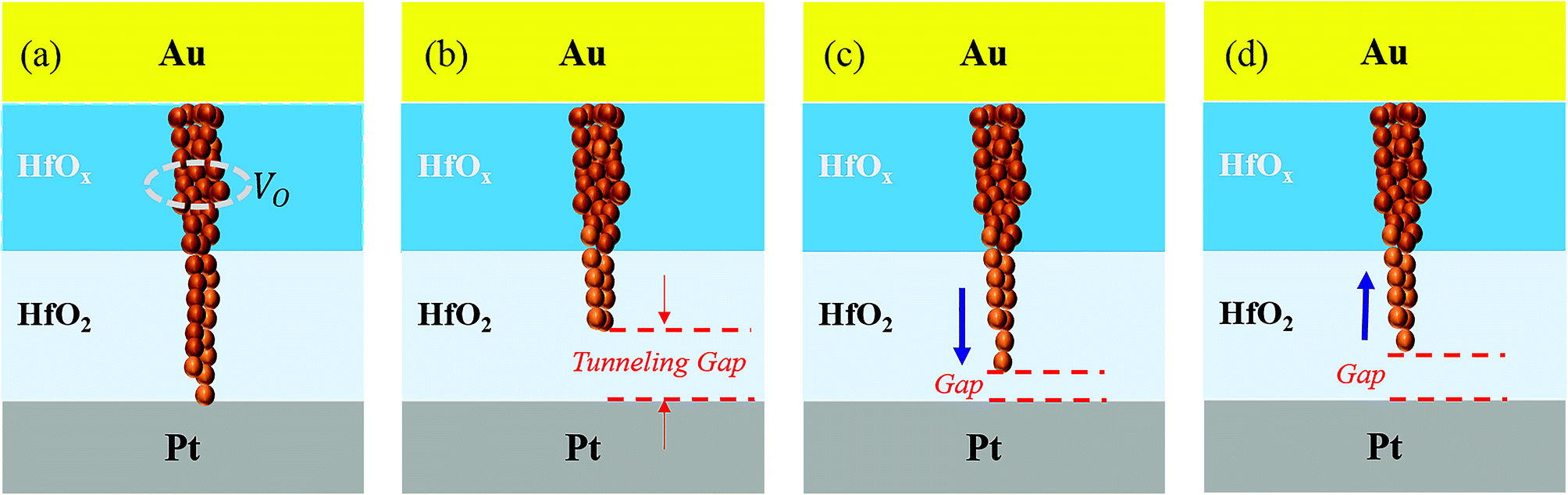 | ||
| Fig. 8 Schematic view of the possible mechanism of the multiple resistance level. (a) Forming process. (b) Reset process. (c) Positive pulse train. (d) Negative pulse train. | ||
The device conductivity can be regulated by tuning the duty cycle of identical pulse (or pulse width) of the applied voltage pulses.42 The relationship between the device current and the duty cycle is depicted in Fig. 9. The duty cycle of identical pulses with 50 μs pulse width are set to 10 μs/50 μs, 20 μs/50 μs and 40 μs/50 μs with identical positive voltage (+0.12 V) and negative voltage (−0.12 V). The current increases (or decreases) with the increasing duty cycle, as shown in Fig. 9(a) and (b). Based on the aforementioned results, the HfOx/HfO2 homo-bilayer structure can be continuously and reversibly varied from dielectric to conductor by modulating the oxygen content, which is appropriate for the dynamic response to input signals. Fig. 9(c) shows the current response to a series of 50 positive voltage pulses (+0.15 V, 20 μs) immediately followed by 50 negative voltage pulses (−0.15 V, 20 μs). The current increase under the stimulation of consecutive positive voltage pulses, conversely, the current decrease under the stimulation of consecutive negative voltage pulses, which can imitate the LTP and LTD function of the biological synapse. Such behavior can be attributed to the accumulation and annihilation process of VO.43 It is noted that the gap emerged between the final state of the positive pulses and the initial state of the negative pulses, which is related to the identical directions of the oxygen ion diffusion and migration.19 The amount of drifting VO increases with the pulse number,44 therefore the steadily accumulated VO gradually form the CFs (incomplete filament) before the abrupt set process when applying the positive pulse voltage. Hence, the resistance of the device can gradually decrease with the increased pulse number. In virtue of the gradual reset process in the HfOx/HfO2 homo-bilayer structure, the resistance of the device depends on the proportion of filament that dissociates under negative pulse voltage. Therefore, the resistance gradually increases with the increased pulse number when the negative voltages pulses were applied on the device, which corresponds to the depression process.
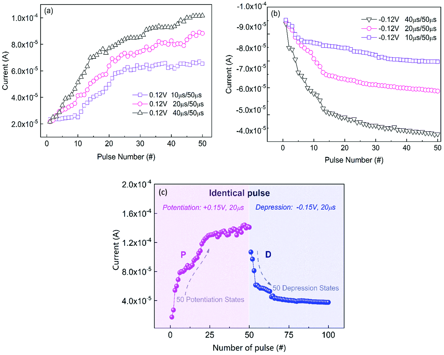 | ||
| Fig. 9 (a) Conductance enhancement and (b) conductance attenuation by consecutive 50 pulse trains in the positive and negative direction under different duty cycle. (c) Potentiation and depression properties under identical positive and negative pulses. | ||
Conclusions
In summary, the resistive switching characteristics of the HfOx/HfO2 bilayer heterostructure were investigated, in which the oxygen content in HfOx layer was modified by varying the Ar/O2 ratios during the deposition process. Stoichiometric ratios of the HfOx layer were estimated by the XPS analysis. Compared with other samples, the HfOx layer deposited under Ar/O2 ratio of 12:2 in the HfOx/HfO2 bilayer heterostructure showed the improved switching performance, which is pretty important to the nonvolatile application. The nonlinear transmission characteristics of the device were investigated, and the modulation of conductance is owing to the result of the motion of oxygen vacancies between oxygen-rich and oxygen-deficient layers. In the simulation process of the biological synapse, multiple resistance levels of the device were obtained in the continuous pulse number, which indicates that the Au/HfOx/HfO2/Pt can dynamically response to the change caused by input signals and have the basic transmission characteristics of the synapse.
Conflicts of interest
There are no conflicts to declare.Acknowledgements
This work was financially supported by the Research Fund of the State Key Laboratory of Solidification Processing (NWPU), China (Grant No. 155-QP-2016), the Fundamental Research Funds for the Central Universities (No. 3102018gxc017) and the Natural Science Basic Research Plan in Shaanxi Province of China (No. 2018JM5059).Notes and references
- R. Waser and M. Aono, Nat. Mater., 2007, 6, 833–840 CrossRef CAS PubMed.
- Y. S. Fan, P. T. Liu, L. F. Teng and C. H. Hsu, Appl. Phys. Lett., 2012, 101, 052901 CrossRef.
- X. Zhu, W. Su, Y. Liu, B. Hu, L. Pan, W. Lu, J. Zhang and R. W. Li, Adv. Mater., 2012, 24, 3941–3946 CrossRef CAS PubMed.
- K. Park and J. S. Lee, RSC Adv., 2016, 6, 21736–21741 RSC.
- G. Niu, M. A. Schubert, S. U. Sharath, P. Zaumseil, S. Vogel, C. Wenger, E. Hildebrandt, S. Bhupathi, E. Perez, L. Alff, M. Lehmann, T. Schroeder and T. Niermann, Nanotechnology, 2017, 28, 215702 CrossRef CAS PubMed.
- J. H. Yoon, K. M. Kim, S. J. Song, J. Y. Seok, K. J. Yoon, D. E. Kwon, T. H. Park, Y. J. Kwon, X. L. Shao and C. S. Hwang, Adv. Mater., 2015, 27, 3811–3816 CrossRef CAS PubMed.
- W. Banerjee, X. Zhang, Q. Luo, H. Lv, Q. Liu, S. Long and M. Liu, Adv. Electron. Mater., 2018, 4, 1700561 CrossRef.
- Y. D. Lin, P. S. Chen, H. Y. Lee, Y. S. Chen, S. Z. Rahaman, K. H. Tsai, C. H. Hus, W. S. Chen, P. H. Wang, Y. C. King and C. J. Lin, Nanoscale Res. Lett., 2017, 12, 407 CrossRef PubMed.
- S. Lee, D. Lee, J. Woo, E. Cha, J. Park and H. Hwang, IEEE Electron Device Lett., 2014, 35, 1022–1024 CAS.
- C. H. Huang, T. S. Chou, J. S. Huang, S. M. Lin and Y. L. Chueh, Sci. Rep., 2017, 7, 2066 CrossRef PubMed.
- Y. C. Chen, C. Y. Lin, H. C. Huang, S. Kim, B. Fowler, Y. F. Chang, X. H. Wu, G. B. Xu, T.-C. Chang and J. C. Lee, J. Phys. D: Appl. Phys., 2018, 51, 055108 CrossRef.
- J. Woo, K. Moon, J. Song, S. Lee, M. Kwak and J. Park, IEEE Electron Device Lett., 2016, 37, 994–997 CAS.
- S. H. Jo, T. Chang, I. Ebong, B. B. Bhadviya, P. Mazumder and W. Lu, Nano Lett., 2010, 10, 1297–1301 CrossRef CAS PubMed.
- G. S. Snider, Nanotechnology, 2007, 18, 365202–365213 CrossRef.
- K. Seo, I. Kim, S. Jung, M. Jo, S. Park and J. Park, Nanotechnology, 2011, 22, 254023 CrossRef PubMed.
- S. Ambrogio, S. Balatti, F. Nardi, S. Facchinetti and D. Ielmini, Nanotechnology, 2013, 24, 384012 CrossRef CAS PubMed.
- T. Ohno, T. Hasegawa, T. Tsuruoka, K. Terabe, J. K. Gimzewski and M. Aono, Nat. Mater., 2011, 10, 591–595 CrossRef CAS PubMed.
- F. Zeng, S. Li, J. Yang, F. Pan and D. Guo, RSC Adv., 2014, 4, 14822–14828 RSC.
- Q. W. Zhong, Y. X. Hai, H. L. Xing, Y. Hao, C. L. Yi and J. Z. Xiao, Adv. Funct. Mater., 2012, 22, 2759–2765 CrossRef.
- S. Q. Wang and J. W. Mayer, J. Appl. Phys., 1988, 64, 4711–4716 CrossRef CAS.
- W. Zhang, J. Z. Kong, Z. Y. Cao, A. D. Li, L. G. Wang and L. Zhu, Nanoscale Res. Lett., 2017, 12, 393 CrossRef PubMed.
- A. Padovani, L. Larcher, O. Pirrotta, L. Vandelli and G. Bersuker, IEEE Trans. Electron Devices, 2015, 62, 1998–2006 CAS.
- K. G. Young-Fisher, G. Bersuker, B. Butcher, A. Padovani, L. Larcher and D. Veksler, IEEE Electron Device Lett., 2013, 34, 750–752 CAS.
- X. Y. Li, X. L. Shao, Y. C. Wang, H. Jiang, C. S. Hwang and J. S. Zhao, Nanoscale, 2017, 9, 2358 RSC.
- M. Akbari, M. K. Kim, D. Kim and J. S. Lee, RSC Adv., 2017, 7, 16704–16708 RSC.
- Z. Wang, P. B. Griffin, J. Mcvittie, S. Wong, P. C. Mcintyre and Y. Nishi, IEEE Electron Device Lett., 2006, 28, 14–16 Search PubMed.
- Y. C. Chen, C. Y. Lin, H. C. Huang, S. Kim, B. Fowler, Y. F. Chang, X. H. Wu, G. B. Xu, T.-C. Chang and J. C. Lee, J. Phys. D: Appl. Phys., 2018, 51, 055108 CrossRef.
- B. Gao, J. F. Kang, H. W. Zhang, B. Sun, B. Chen, L. F. Liu, R. Q. Han and Y. Y. Wang. Solid-state Device Research Conference. IEEE, 2010, pp. 392–395 Search PubMed.
- T. Ninomiya, T. Takagi, Z. Wei, S. Muraoka, R. Yasuhara, K. Katayama, Y. Ikeda, K. Kawai, Y. Kato, Y. Kawashima, S. Ito, T. Mikawa, K. Shimakawa and K. Aono, VLSI Technology. IEEE, 2012, pp. 73–74 Search PubMed.
- H. Tian, W. Mi and H. Zhao, Nanoscale, 2017, 9, 9275–9283 RSC.
- L. Zhao, H. Y. Chen, S. C. Wu, Z. Jiang, S. Yu, T. H. Hou, H. S. P. Wong and Y. Nishi, Nanoscale, 2014, 6, 5698 RSC.
- Y. Matveyev, R. Kirtaev, A. Fetisova, S. Zakharchenko, D. Negrov and A. Zenkevich, Nanoscale Res. Lett., 2016, 11, 147 CrossRef PubMed.
- D. Kuzum, S. Yu and H. S. P. Wong, Nanotechnology, 2015, 24, 382001 CrossRef.
- B. Gao, L. Liu and J. Kang, Prog. Nat. Sci.: Mater. Int., 2015, 25, 47–50 CrossRef CAS.
- M. Akbari, M. K. Kim, D. Kim and J. S. Lee, RSC Adv., 2017, 7, 16704–16708 RSC.
- H. Lv, H. Wan and T. Tang, IEEE Electron Device Lett., 2010, 31, 978–980 CAS.
- B. Gao, H. W. Zhang, S. Yu, B. Sun, L. F. Liu, X. Y. Liu, Y. Wang, R. Q. Han, J. F. Kang, B. Yu and Y. Y. Wang, VLSI Symp., IEEE, 2009, pp. 30–31 Search PubMed.
- J. Woo, K. Moon, J. Song, M. Kwak, J. Park and H. Hwang, IEEE Trans. Electron Devices, 2016, 63, 5064–5067 CAS.
- G. Niu, M. A. Schubert, S. U. Sharath, P. Zaumseil, S. Vogel, C. Wenger, E. Hildebrandt, S. Bhupathi, E. Perez, L. Alff, M. Lehmann, T. Schroeder and T. Niermann, Nanotechnology, 2017, 28, 215702 CrossRef CAS PubMed.
- F. Nardi, S. Larentis, S. Balatti, D. C. Gilmer and D. Ielmini, IEEE Trans. Electron Devices, 2012, 59, 2461–2467 CAS.
- G. Sassine, S. L. Barbera, N. Najjari, M. Minvielle, C. Dubourdieu and F. Alibart, J. Vac. Sci. Technol., B: Nanotechnol. Microelectron.: Mater., Process., Meas., Phenom., 2016, 34, 012202 Search PubMed.
- B. Gao, B. Chen, Y. Chen, L. Liu, X. Liu and R. Han, Pulse voltage dependent resistive switching behaviors of HfO-based RRAM, IEEE, 2010 Search PubMed.
- Y. Matveyev, K. Egorov, A. Markeev and A. Zenkevich, J. Appl. Phys., 2015, 117, 382001–382083 CrossRef.
- J. Woo, K. Moon, J. Song, S. Lee, M. Kwak and J. Park, IEEE Electron Device Lett., 2016, 37, 994–997 CAS.
| This journal is © The Royal Society of Chemistry 2018 |