
 Open Access Article
 This Open Access Article is licensed under a Creative Commons Attribution-Non Commercial 3.0 Unported Licence
Enhanced photoresponse of a high-performance self-powered UV photodetector based on ZnO nanorods and a novel electrolyte by the piezo-phototronic effect†
Xiaoli Penga,
Weihao Wanga,
Yiyu Zenga,
Xinhua Pan *a,
Zhizhen Ye*a and
Yujia Zengb
*a,
Zhizhen Ye*a and
Yujia Zengb
aState Key Laboratory of Silicon Materials, Cyrus Tang Center for Sensor Materials and Applications, School of Materials Science and Engineering, Zhejiang University, Hangzhou 310027, People's Republic of China. E-mail: panxinhua@zju.edu.cn; yezz@zju.edu.cn; Fax: +86 571 87952124; Tel: + 86 571 87952187
bShenzhen Key Laboratory of Laser Engineering, College of Optoelectronic Engineering, Shenzhen University, Shenzhen 518060, People's Republic of China
First published on 26th September 2018
Abstract
A flexible self-powered ultraviolet (UV) photodetector based on ZnO nanorods (NRs) and a novel iodine-free quasi solid-state electrolyte was fabricated. The obtained device has a fast and high response to UV light illumination at zero bias and also shows long-term stability. The responsivity is 50.5 mA W−1 and the response time is less than 0.2 s. Strain-induced piezo-phototronic potential within wurtzite-structured ZnO can optimize the performance of corresponding optoelectronic devices since it could effectively tune the charge carriers' separation and transport. The photoresponse performances of the photodetector under different upward angles (tensile strain) and downward angles (compressive strain) at 0 V bias were studied in detail. A 163% change of responsivity was obtained when the downward angle reached 60°. The enhancement could be interpreted by the piezo-phototronic effect. The piezoelectric potential (piezopotential) at the ZnO NRs/electrolyte interface can expand the built-in field, and as a result, it is easier for charge carriers to separate and transport.
Introduction
Over the past few years, nanostructured materials have been extensively investigated for their promising applications in the optoelectronics field. Zinc oxide (ZnO) is a good candidate for optoelectronic applications, due to its wide direct bandgap (∼3.37 eV), large exciton binding energy (∼60 meV), high carrier mobility, environmental friendliness and high resistance irradiation.1–3 Especially, ZnO nanorods (NRs) have a high aspect ratio for carrier transport and diffusion, providing a pathway for light absorption in the near ultraviolet (UV) regions, which is suitable to be used as a UV photodetector without extra filters.4–6 Until now, various types of UV photodetectors based on ZnO NRs have been researched such as p–n junction, metal-semiconductor-metal, Schottky junction and so on.7–13 Among them, Schottky junction type UV photodetectors based on a ZnO NRs/electrolyte shows practical performance without a complex epitaxial process.11 When ZnO NRs contact with the electrolyte, a built-in electric field, in other words, the Schottky barrier is formed. The Schottky barrier acts as the driving force to separate the generated electron–hole pairs, which makes the device operate in harsh environments without external power.As for electrolytes, various electrolytes have been investigated. Traditionally, organic liquid electrolyte containing I−/I3− is favored because of its high conductivity.14 While the liquid electrolyte is incline to leak out and evaporate, which results in low long-term stability and difficulty in sealing. Besides, the iodine in the electrolyte is easy to corrode the electrode and sublimate, which has a negative effect on the device. Thus, iodine-free ionic quasi solid-state electrolytes have drawn researchers' interest, since they can simultaneously hinder cohesive property of a solid and diffusive property of a liquid, and also they are environment friendly.15,16 A proper metal salt is usually added into the quasi solid-state electrolytes to improve the photoelectric performance and to coordinate with polymeric ionic liquid electrolyte to improve the solubility of solvent.17 Nevertheless, ZnO NRs/iodine-free ionic quasi solid-state electrolyte photodetector has seldom been investigated, in particular the flexible photodetector, which has great potential using in wearable devices.
In recent years, piezo-phototronic effect in ZnO has been utilized to enhance the performance of optoelectronic devices.18–23 Since ZnO is a non-central symmetric wurtzite, a piezopotential is created inside the crystal, when applying strain along the c-axis. Taking advantage of the strain induced piezo-phototronic effect, the charge carrier transport behavior across a Schottky junction could be effectively tuned. Zhang et al. reported a UV photodetector which shows an enhanced UV sensing capability on externally applying tensile strains, unfortunately, the UV sensing performance was still poor; the responsivity was only 0.8 mA W−1 at 0 V on a 0.753% tensile strain.11
In this work, a flexible self-powered UV photodetector was successfully fabricated based on the ZnO NRs and an iodine-free quasi solid-state electrolyte containing potassium iodide (KI), polyethylene oxide (PEO) and 1-methyl-3-propylimidazolium iodide (PMII). The photodetector shows large photocurrent, fast photoresponse speed and high responsivity at zero bias. Besides, the photoresponse performances of the photodetector under different upward angles (tensile strains) and downward angles (compressive strains) at 0 V bias were studied in detail. We used the energy band diagrams of the device with and without strain to interpret the strain-modulated mechanism.
Experimental
Synthesize ZnO NRs on polyethylene terephthalate (PET) substrate
All the chemicals in this work were of analytical grade and used directly without any further purification. Commercial flexible indium-doped tin oxide (ITO) coated PET (sheet resistance is 6 ohm sq−1 and the thickness is 125 μm) was used as the substrate. The flexible substrate was cleaned with acetone, ethanol and deionized water in sequence each for 30 minutes. Before the deposition process, the flexible substrate was cleaned by N2 and part of the substrate was covered by the Kapton tape to serve as the electrode. A ZnO seed layer was deposited on the ITO coated PET substrate by pulsed laser deposition (PLD) for 10–15 minutes at room temperature. The oxygen pressure and energy of the laser are 1 Pa and 300 mJ, respectively. Then, ZnO NRs were prepared by a simple hydrothermal method.24–26 The coated substrate with the coating side upside-down was immersed in a growth solution including 20 mM zinc nitrate and 20 mM hexamethylenetetramine (C6H12N4, HMT) loaded in a Teflon liner stainless-steel autoclave at 85 °C for 4–5 h. After the reaction was complete, the as-grown ZnO NRs were thoroughly rinsed with ethanol and deionized water carefully followed by a drying step in an oven at 60 °C overnight.Preparation of quasi solid-state electrolytes
The iodine-free quasi solid-state electrolyte was prepared by dissolving 50 mg of PMII in 2.5 ml acetonitrile, and stirred for about 30 min. 0.03 g KI was added into the above solution under stirring. Afterwards, 0.2 g PEO was added and stirred overnight to obtain the desired homogeneous electrolyte. The electrolyte solutions were kept under stirring for about 1 h before each measurement to assure the electrolyte homogeneous.17Device fabrication and characterization
30 μl of the PMII-based quasi solid-state electrolyte was dropped onto the as-grown ZnO NRs and spun at a rate of 3000 rpm for 30 s, repeating three times. A 20 nm thick Pt film was then deposited on the ITO-PET substrate by electron beam evaporation, serving as the counter electrode. A PET-based sealant material was used to bind the two electrodes together. The active area of the UV device was 1 × 1 cm2. The schematic diagram of the device structure is presented in Fig. S1 in the ESI.† All the measuring procedures are under the same testing condition. The morphology and structure of the samples were characterized by a field emission scanning electron microscopy (FE-SEM Hitachi S-4800). The temporal response of the UV detector was measured by illuminating the devices with a UVA-LED. The UV-vis absorption spectra were recorded with a spectrophotometer (UV-3600). The current–voltage (I–V) characteristics were measured using an Agilent E5270B parameter analyzer under ambient conditions.Results and discussion
Fig. 1(a) shows the SEM image of ZnO seed layer on ITO coated PET substrate. ZnO seed particles are uniform and dense, which is beneficial for obtaining uniform ZnO NRs. The typical top-view SEM image and cross-sectional view of ZnO NRs are shown in Fig. 1(b) and (c), respectively. The ZnO NRs show typical hexagonal morphology and grow epitaxially on the PET substrate with preferred c-orientation due to the existence of the pre-deposition of the ZnO seed layer. The ZnO NRs exhibit vertical and uniform with an average length of ∼0.81 μm and a diameter of ∼60 to 130 nm. It can be seen that gaps are well distributed between the ZnO NRs, which facilitate the penetration of the electrolyte. The UV-vis absorbance spectrum of ZnO NR is shown in Fig. 1(d), which clearly shows that it has a significant absorption below a wavelength of 400 nm. As for a direct band gap material, the absorption coefficient α as a function of photon energy hυ can be determined as:| (αhυ)2 = A(hυ − Eg) | (1) |
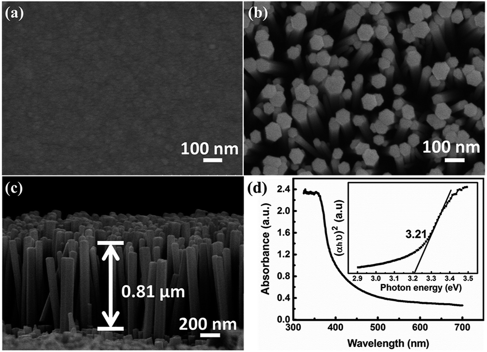 | ||
| Fig. 1 (a) SEM image of ZnO seed layer on ITO coated PET substrate, (b) the top-view SEM image of ZnO NRs, (c) the cross-sectional view of ZnO NRs, (d) the UV-vis absorbance spectrum of ZnO NRs. The inset is the corresponding band gap values derived from extrapolating the graph of (αhυ)2 vs. (hυ − Eg). | ||
The XRD pattern of ZnO NRs is presented in Fig. S2 in the ESI.† In addition to the substrate diffraction peaks, there is a sharp diffraction peak at 34.4°, corresponding to the (002) crystal plane of wurtzite ZnO phase (JCPDS No. 36-1451), indicating that ZnO NRs have a good c-axis preferred orientation, which further confirms the results of SEM.
To further investigate the photoelectric properties of the UV detector, the I–V characteristics curves both in dark conditions and the illumination of UV light with a power density of 60 μW cm−2 (λ = 365 nm) are shown in Fig. 2(a). I–V curves of the device both in darkness and illumination display a Schottky barrier like behavior, reflecting that the heterojunction structure has been successfully obtained. At 0 V, there is an obvious difference between dark current and photocurrent, indicating its self-powered mode of operation. The Schottky barrier acts as the driving force to separate the generated electron–hole pairs. The responsivity (R) is used to indicate the photocurrent efficiency. It is determined as:
 | (2) |
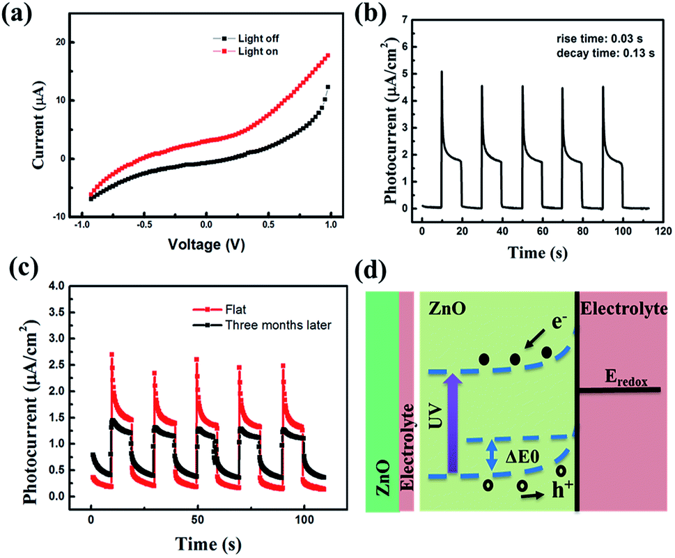 | ||
| Fig. 2 (a) I–V characteristics of the as-fabricated UV detector under dark conditions and the illumination of UV light. The power of the UV light used in all the experiments is 60 μW cm−2 (λ = 365 nm). (b) The photocurrent response of the device at the zero bias. Five repeated cycles of switching UV light on (10 s) and off (10 s) were recorded. (c) Photocurrent response of a UV detector three months later. (d) Energy band bending of the device and the self-powered sensing mechanism at the zero bias. | ||
Fig. 2(b) shows photocurrent response of the UV detector, which was measured at 0 V under an intermittent irradiation of 365 nm UV light. Five repeated cycles of switching the 60 μW cm−2 UV light on (10 s) and off (10 s) were recorded. Interestingly, there are two stages in each cycle of the curves. In the first stage, a sharp current peak emerged as soon as the UV light turned on. In the second stage, the photocurrent decreased quickly at first and then reached a steady plateau until turned off the light. We have demonstrated that this phenomenon had little to do with the stability of UV light (the photoresponse of covering sample and uncovering sample are presented in Fig. S3 in the ESI†). We designed a comparative experiment including two groups to illustrate this. For group 1, we just switched the light on (10 s) and off (10 s) and recorded the photocurrent response. For group 2, at first, we turned on the light and at the same time used a black board to block the light until the light was stable. Then we removed the black board and recorded the photocurrent response. We could see that there was no difference between the two curves, reflecting that this “two-stages phenomenon” might mainly origin from the material. From a previous report, owing to the non-central symmetric crystal structures of wurtzite ZnO, temperature changes will induce pyroelectric potentials across ZnO.32,33 The sharp peaks might stem from the combination of photovoltaic and pyroelectric effect under the UV light. While in the second stage, the photocurrent reached steady because the pyroelectric potential disappeared as the temperature stayed constant. Noting that the photocurrent of the first and the second stage are 4.55 × 10⁻⁶ A cm−2 and 2.05 × 10⁻⁶ A cm−2, respectively, indicating 220% increasing on photocurrent by pyroelectric effect. In each cycle, the photocurrent had no distinct degradation and the response process was fast. In fact, the response time is a critical parameter for the practical application of a UV photodetector. Correspondingly, the rise and decay time are 0.03 and 0.13 s, respectively, which is shorter than the values published previously, indicating a rapid photo response behavior at 0 V bias.34,35 To illustrate the stability of the device, Fig. 2(c) depicts photoresponse curves of a sample and the same sample three months later. In each cycle, there is no apparent decay on photoresponse. The rise and decay time are 0.04 s and 0.14 s, respectively. Three months later, the rise and decay time are 0.34 s and 0.60 s, which suggest no distinct difference, indicating good time stability. Nevertheless, the photocurrent is ∼1.25 × 10⁻⁶ A cm−2, which is slightly smaller than the value (∼1.55 × 10⁻⁶ A cm−2) three months ago. This is because part of the solvent has volatilized inevitably, resulting in the decrease of charge carrier in the electrolyte. In the electrolyte, PEO is used to solidify the liquid electrolyte to obtain the quasi solid-state electrolyte. Thus, the electrolyte is hard to volatilize and easy to be sealed. Anyhow, the quasi solid-state electrolyte is comparably stable. Compared with liquid electrolyte, it is easier to seal and harder to leak out. It should be noted that pyroelectric effect measured three months later is negligible compared with that measured three months ago. This phenomenon attributes to the environment temperature, since the environment temperature has a great impact on pyroelectric effect, the higher the temperature, the lower the pyroelectric effect.
The potential mechanism of UV photodetector at 0 V is shown in the Fig. 2(d). The Fermi level (Ef) of ZnO is higher than the redox potential of the electrolyte (Eredox). When ZnO NRs contact with electrolyte in the dark, electrons diffuse from ZnO NRs to electrolyte and holes diffuse in the opposite direction. As a result, a built-in electric field orienting from ZnO NRs to electrolyte is formed, and the band bending at the interface between ZnO NRs and the electrolyte. When the UV light (365 nm) illuminates on the device, electron is excited from valence band (VB) to conduction band (CB), leaving behind a hole. Subsequently, the generated electron–hole pairs are forced to separate by the built-in electric field. On one hand, the holes migrate to the ZnO NRs/electrolyte interface and get captured by the I− in the electrolyte (h+ + I− → I3−). On the other hand, the electrons travel along the ZnO NRs to FTO, and then transfer to the Pt layer of counter electrode through the external circuit. The I3− is reduced to I− at the counter electrode by the electrons (I3− + e− → I−). In this process, the circuit can keep running without any external bias. Besides, compared with the traditional electrolyte, the device can work smoothly without I2 avoiding the corrosiveness and sublimate of I2. What's more, the photocurrent can be generated repeatedly (due to the photovoltaic effect).
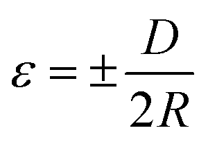
As has been reported in previous works, piezo-phototronic polarization at the interface could tune the band structure and change transport properties without changing the interface structure.36–38 Here, the strain effect on the UV photodetector was further investigated. By applying different bending curvatures, the strain can be calculated as39
 | (3) |
The photocurrent response curves of the device under varying downward angles (compressive strains) at zero bias are shown in Fig. 3(a). The photocurrent increases step by step with the increasing of the downward angles, namely, the compressive strains. To further investigate the strain modulation on the performance of the UV photodetector, we plotted the curves of the responsivity versus angles in Fig. 3(b). The responsivity increases monotonically with the increase of the curving angles, and about 63% enhanced responsivity can be got when the curving angles up to 60°. The response time is another key parameter for a UV photodetector. We can see from Fig. 3(a) that there is no obvious decay in response time when increasing the angles. That is, increasing the angles can increase the responsivity of the device owing to the piezo-phototronic effect, while does not harm the response time. To reveal the mechanism of the strain-enhanced performance of the device, we test the I–V characteristics of the device under different angles, as shown in Fig. 3(c) (inset), exhibiting Schottky barrier behavior. The threshold voltage increases with the increased angles. We also calculated the change of Schottky barrier height (SBH) through thermionic emission model. According to the thermionic emission model, the reverse saturation current I0 can be expressed40
 | (4) |
 | (5) |
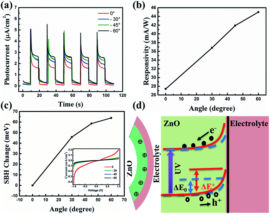 | ||
| Fig. 3 (a) Photocurrent response curves of the device under varying angles (compressive strains) at zero bias. (b) The responsivity as a function of angles. (c) Derived SBH change with variable angles; (inset) I–V characteristics under different angles. (d) Schematic energy band structure of the device with and without the presence of a negative piezopotential, as shown in solid red and dotted blue lines, respectively. | ||
The SHB change with variable angles is plotted in Fig. 3(c), revealing that the SHB change increases with the increased angles, which promotes the separation and extraction of the photo generated electro–hole pairs and thus increases the photocurrent of the device. The schematic energy band structure of the device with and without the presence of a negative piezopotential is shown in Fig. 3(d). Owing to the preferred +c-orientation growth of ZnO NRs, a negative piezopotential will be induced at the interface, repelling electrons away from the interface and consequently further depleting the interface and raising the barrier height from ΔE0 to ΔE+. The increased barrier height broadens the depletion region and strengthens the built in electric field. As a result, more carriers can be separated more effectively, leading to the enhanced responsivity.
Furthermore, since the polarity of the piezopotential relies on the relationship between direction of c-axis of ZnO NRs and applied strain, when applying tensile strain on ZnO NRs, a positive piezopotential will be created at the interface of the ZnO NRs and the electrolyte. To investigate this phenomenon, we changed the angles upward and measured the photocurrent response at zero bias with the UV light switching on and off, as shown in Fig. 4(a). As shown in Fig. 4(b), the responsivity decreased with the increasing of the upward angles. The SBH is plotted in Fig. 4(c), and it declined as the decreasing of the upward angles. We use the schematic of energy band structure to explain this phenomenon, as presented in Fig. 4(d). A positive piezopotential will be created at the interface under upward angles, which causes electrons to accumulate at the interface, resulting in a narrower depletion layer and a lower barrier height from ΔE0 to ΔE−. The decreased barrier height weakened the built in electric field. Thus, the recombination of the generated electron–hole pairs could be increased, resulting in the decreased responsivity. Electron–hole pairs could be increased, resulting in the decreased responsivity.
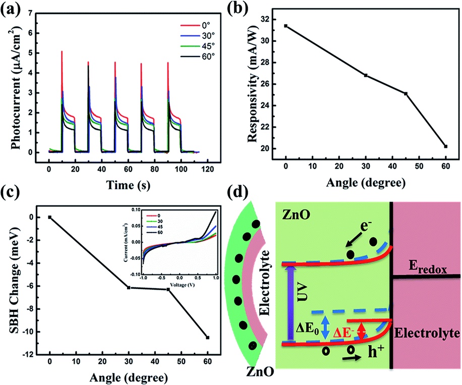 | ||
| Fig. 4 (a) Photocurrent response curves of the device under varying angles (tensile strains) at zero bias. (b) The responsivity as a function of angles. (c) Derived SBH change with variable angles; (inset) I–V characteristics under different angles. (d) Schematic energy band structure of the device with and without the presence of a positive piezopotential, as shown in solid red and dotted blue lines, respectively. | ||
Conclusions
In summary, we successfully prepared the ZnO NRs on ITO coated PET substrate by a facile hydrothermal method. A flexible, stable, low-cost and self-powered UV photodetector is fabricated based on ZnO NRs and a novel iodine-free quasi solid-state electrolyte, which shows fast and high response to UV light at 0 V. The rise and decay time are 0.03 and 0.13 s, respectively. The responsivity is 50.5 mA W−1. The stain-induced piezopotential on the performance of the ZnO NRs/electrolyte was investigated in detail. About 63% enhanced responsivity could be achieved when the downward angles up to 60°. The enhancement mechanism is attributed to more favorable separation and transport of photogenerated electron–hole pairs, which is a result of the modification effect of the negative piezopotential on the band structure at the interface between the ZnO NRs and the electrolyte. Moreover, the device exhibits good stability, and the performance has no obvious decay three months later. This work provides a guideline to further optimize the performance of a self-powered UV photodetector based on ZnO NRs and an iodine-free quasi solid-state electrolyte via strain engineering.Conflicts of interest
There are no conflicts to declare.Acknowledgements
This work was supported by National Natural Science Foundation of China under Grant No. 51302244 and 91333203, and Zhejiang Provincial Natural Science Foundation of China under Grant No. LY17E020005.References
- U. Ozgur, Y. I. Alivov, C. Liu, A. Teke, M. A. Reshchikov, S. Dogan, V. Avrutin, S. J. Cho and H. Morkoc, J. Appl. Phys., 2005, 98, 041301 CrossRef.
- Z. L. Wang, J. Phys.: Condens. Matter, 2004, 16, R829–R858 CrossRef CAS.
- C. Klingshirn, ChemPhysChem, 2007, 8, 782–803 CrossRef CAS PubMed.
- A. B. Djurišić and Y. H. Leung, Small, 2006, 2, 944–961 CrossRef PubMed.
- Y. K. Su, S. M. Peng, L. W. Ji, C. Z. Wu, W. B. Cheng and C. H. Liu, Langmuir, 2010, 26, 603–606 CrossRef CAS PubMed.
- A. B. Djurišić, A. M. C. Ng and X. Y. Chen, Prog. Quantum Electron., 2010, 34, 191–259 CrossRef.
- S. M. Hatch, J. Briscoe and S. Dunn, Adv. Mater., 2013, 25, 867–871 CrossRef CAS PubMed.
- P. Lin, X. Chen, X. Yan, Z. Zhang, H. Yuan, P. Li, Y. Zhao and Y. Zhang, Nano Res., 2014, 7, 860–868 CrossRef CAS.
- S. I. Inamdar and K. Y. Rajpure, J. Alloys Compd., 2014, 595, 55–59 CrossRef CAS.
- W. Dai, X. Pan, S. Chen, C. Chen, Z. Wen, H. Zhang and Z. Ye, J. Mater. Chem. C, 2014, 2, 4606 RSC.
- Y. W. Shen, X. Q. Yan, H. N. Si, P. Lin, Y. C. Liu, Y. H. Sun and Y. Zhang, ACS Appl. Mater. Interfaces, 2016, 8, 6137–6143 CrossRef CAS PubMed.
- Z. Gao, W. Jin, Y. Zhou, Y. Dai, B. Yu, C. Liu, W. Xu, Y. Li, H. Peng, Z. Liu and L. Dai, Nanoscale, 2013, 5, 5576 RSC.
- P. Ni, C. Shan, S. Wang, X. Liu and D. Shen, J. Mater. Chem. C, 2013, 1, 4445–4449 RSC.
- A. Berendjchi, R. Khajavi, A. A. Yousefi and M. E. Yazdanshenas, J. Cleaner Prod., 2017, 149, 521–527 CrossRef CAS.
- W. Cho, Y. R. Kim, D. Song, H. W. Choi and Y. S. Kang, J. Mater. Chem. A, 2014, 2, 17746–17750 RSC.
- N. Sharifi, F. Tajabadi and N. Taghavinia, ChemPhysChem, 2014, 15, 3902–3927 CrossRef CAS PubMed.
- X. Peng, Y. Zeng, X. Pan, W. Wang, Y. Zhou, F. Wang, Q. Lu and Z. Ye, RSC Adv., 2017, 7, 29440–29445 RSC.
- S. Jeong, M. W. Kim, Y. Jo, Y. Leem, W. Hong, B. Kim and S. Park, Nano Energy, 2016, 30, 208–216 CrossRef CAS.
- X. Wang, J. Zhou, J. Song, J. Liu, N. Xu and Z. L. Wang, Nano Lett., 2006, 6, 2768–2772 CrossRef CAS PubMed.
- Z. L. Wang, Nano Today, 2010, 5, 540–552 CrossRef CAS.
- Z. L. Wang, J. Phys. Chem. Lett., 2010, 1, 1388–1393 CrossRef CAS.
- Z. L. Wang, Adv. Mater., 2012, 24, 4632–4646 CrossRef CAS PubMed.
- Y. Zhang, X. Yan, Y. Yang, Y. Huang, Q. Liao and J. Qi, Adv. Mater., 2012, 24, 4647–4655 CrossRef CAS PubMed.
- Y. Zeng, Z. Ye, B. Lu, W. Dai and X. Pan, Appl. Phys. A, 2016, 122, 296 CrossRef.
- L. Vayssieres, Adv. Mater., 2003, 15, 464–466 CrossRef CAS.
- S. Xu and Z. L. Wang, Nano Res., 2011, 4, 1013–1098 CrossRef CAS.
- B. Zhao, F. Wang, H. Chen, L. Zheng, L. Su, D. Zhao and X. Fang, Adv. Funct. Mater., 2017, 27, 1700264 CrossRef.
- B. Deka Boruah and A. Misra, ACS Appl. Mater. Interfaces, 2016, 8, 18182–18188 CrossRef CAS PubMed.
- H. Chen, K. Liu, X. Chen, Z. Zhang, M. Fan, M. Jiang, X. Xie, H. Zhao and D. Shen, J. Mater. Chem. C, 2014, 2, 9689–9694 RSC.
- Q. Li, L. Wei, Y. Xie, K. Zhang, L. Liu, D. Zhu, J. Jiao, Y. Chen, S. Yan, G. Liu and L. Mei, Nanoscale Res. Lett., 2013, 8, 415 CrossRef PubMed.
- O. Game, U. Singh, T. Kumari, A. Banpurkar and S. Ogale, Nanoscale, 2014, 6, 503–513 RSC.
- W. Peng, X. Wang, R. Yu, Y. Dai, H. Zou, A. C. Wang, Y. He and Z. L. Wang, Adv. Mater., 2017, 29, 1606698 CrossRef PubMed.
- Z. Wang, R. Yu, C. Pan, Z. Li, J. Yang, F. Yi and Z. L. Wang, Nat. Commun., 2015, 6, 8401 CrossRef CAS PubMed.
- J. Li, X. Wu, M. M. Shirolkar, M. Li, C. Xu and H. Wang, RSC Adv., 2017, 7, 18987–18992 RSC.
- F. Yi, Q. Liao, Y. Huang, Y. Gu and Y. Zhang, Semicond. Sci. Technol., 2013, 28, 105023 CrossRef.
- P. Lin, X. Yan, Y. Liu, P. Li, S. Lu and Y. Zhang, Phys. Chem. Chem. Phys., 2014, 16, 26697–26700 RSC.
- S. Lu, J. Qi, S. Liu, Z. Zhang, Z. Wang, P. Lin, Q. Liao, Q. Liang and Y. Zhang, ACS Appl. Mater. Interfaces, 2014, 6, 14116–14122 CrossRef CAS PubMed.
- P. Lin, X. Yan, Z. Zhang, Y. Shen, Y. Zhao, Z. Bai and Y. Zhang, ACS Appl. Mater. Interfaces, 2013, 5, 3671–3676 CrossRef CAS PubMed.
- R. Yang, Y. Qin, L. Dai and Z. L. Wang, Nat. Nanotechnol., 2009, 4, 34–39 CrossRef CAS PubMed.
- B. K. Sharma, N. Khare and S. Ahmad, Solid State Commun., 2009, 149, 771–774 CrossRef CAS.
Footnote |
| † Electronic supplementary information (ESI) available. See DOI: 10.1039/c8ra05909h |
| This journal is © The Royal Society of Chemistry 2018 |