
 Open Access Article
 This Open Access Article is licensed under a Creative Commons Attribution-Non Commercial 3.0 Unported Licence
Flexible top-emitting organic light emitting diodes with a functional dielectric reflector on a metal foil substrate†
Kihyon Hong *a,
Hak Ki Yub,
Illhwan Leec,
Sungjun Kimc,
Youngho Kimb,
Kisoo Kimc and
Jong-Lam Lee*c
*a,
Hak Ki Yub,
Illhwan Leec,
Sungjun Kimc,
Youngho Kimb,
Kisoo Kimc and
Jong-Lam Lee*c
aDepartment of Materials Science and Engineering, Chungnam National University, Daejeon, Korea. E-mail: khong@cnu.ac.kr
bDepartment of Materials Science and Engineering, Department of Energy System Research, Ajou University, Suwon, Korea
cDepartment of Materials Science and Engineering, Pohang University of Science and Technology, Korea. E-mail: jllee@postech.ac.kr
First published on 20th July 2018
Abstract
For flexible organic light emitting diodes (OLEDs), roll-to-roll production enables low-cost fabrication and wide-ranging applications. Choosing an appropriate substrate material is one of the critical issues in the fabrication of flexible OLEDs. We demonstrated top-emitting OLEDs with a highly reflective distributed Bragg reflector (DBR) using a metal foil substrate. The DBR, made of seven pairs of SiO2/ZrO2, was formed by electron-beam evaporation on metal foil and showed high reflectivity of 90.5% at λ = 500 nm. The DBR served not only as the optical reflector, but also the substrate insulating layer which enabled the electrical isolation and prevented crosstalk. The OLEDs showed an operation voltage of 6.5 V at a current density of J = 10 mA cm−2 and maximum luminance of 17![[thin space (1/6-em)]](https://www.rsc.org/images/entities/char_2009.gif) 400 cd m−2 at J = 225 mA cm−2. The electroluminescence property of the device could be maintained under the tensile bending condition.
400 cd m−2 at J = 225 mA cm−2. The electroluminescence property of the device could be maintained under the tensile bending condition.
Introduction
Organic light emitting diodes (OLEDs) have gained widespread attention for application in optoelectronic devices because they can be applied over a large area, and are lightweight, transparent, and flexible.1,2 For display devices and general lighting, glass has been used as a substrate material of OLEDs because of its transparency, high-temperature processing capability, and smooth surface.3–5 Current studies on OLEDs have been motivated by the potential for low-cost manufacture with high throughput using roll-to-roll (R2R) techniques, for which the glass substrate is unfavourable because of its non-flexibility.6,7 Thus, the flexible substrate materials are an essential prerequisite for performance, reliability, and practical application of flexible OLEDs. Numerous attempts have been made to substitute glass, which is unlikely to be sustainable for flexible devices and the R2R process, including plastic film (e.g. PET, PEN, PI), polymer film (e.g. PDMS), and metal foil with varying success.8–10 Plastic or polymer films have the advantage of excellent flexibility. Thus, the materials can be employed in the R2R process for fabrication of flexible OLEDs and other electronic devices. However, these substrates have the disadvantage of a high water vapour transmission rate (>0.1 g m−2 per day), which limits the stability of OLEDs. In addition, the process temperature is limited. To ensure high-performance OLEDs, the backplane process must be performed at around 300 °C or above. Due to the low glass transition temperature of the materials, significant thermal shrinkage of plastic substrates can occur during the high-temperature process and can degrade the performance and stability of the device. Metal foil can be a good candidate on other substrates because of its various characteristics, including lower chemical sensitivity, lower oxygen and moisture permeability, and high-temperature stability. Thus, various kinds of OLEDs with metal foil substrates have been reported.11,12To employ metal foil for flexible OLEDs, the substrate has been carefully prepared and adjusted, including planarization to reduce surface roughness and electrical passivation to reduce capacitive coupling between the devices and the conductive metal foil. For this preparation, spin-on-glass (SOG) and polymer material have been used. A SOG is a silica particles suspended solution. The SOG can be converted to a SiO2 layer with a dielectric constant of ε = 3–5 during the coating process and it can perform the role of both planarization and electrical passivation. However, the material requires an additional curing process at high temperature (>300 °C) for a long period of time (>60 min) in order to drive out the solvent and achieve the desired property.13,14 Polymer materials such as polyimide and benzocyclobutene are low-k dielectric (ε = 2–3) resins that can be spun on and cured at relatively low temperature (<200 °C). Thus, the coating of these materials can reduce the surface roughness by up to 0.1 μm (peak to peak roughness) and can be used for substrate preparation of OLED and thin film transistors (TFT) backplane. However, the curing process still require a long period (>60 min) and a multi-step coating sequence. Another issue in OLEDs with metal foil substrate is the bottom reflective electrode.15,16 Due to the opaque nature of metal foil, the OLEDs require a top-emitting structure that has a reflective bottom anode. Ag can be used as a bottom reflective electrode material due to its high reflectivity and excellent conductivity.17–19 However, the Ag is not suitable for low voltage operation devices because of its relatively low work function (WF = 4.3 eV) as an anode. Therefore, to achieve R2R processed flexible OLEDs on metal foil, the development of simple and cost effective substrate coating (electrical passivation) materials and bottom reflective electrode materials should be considered.
Here, we demonstrate flexible top-emitting OLEDs (TOLEDs) with highly reflective distributed Bragg reflector (DBR) on a metal foil substrate. The novelty of this work, with respect to the previous reports, is that we demonstrated flexible OLEDs with DBR on a metal foil substrate. The highly reflective DBR formed on metal foil resulted in enhancement of optical property of OLEDs. At the same time, the DBR served as a substrate insulating layer; thus, the fabrication process can be simple when compared with that of OLEDs on metal foil substrate prepared with additional surface planarization and electrical passivation process. The optimal DBR structure was designed by optical simulation and the DBR based on seven pairs of SiO2/ZrO2 multilayer fabricated by an electron beam (e-beam) evaporation process showed a high reflectivity value of 90.5% at λ = 500 nm. Because this DBR is composed of a dielectric multilayer, devices can be directly fabricated on the substrate without an additional insulating process such as an insulating layer coating and high temperature curing process. Thus, in the presented work, the DBR films played dual roles of electrical passivation and reflective mirror. The TOLEDs with DBR mirror showed an operation voltage of 6.5 V at current density of J = 10 mA cm−2 and maximum luminance of 17400 cd m−2 at J = 225 mA cm−2. We also evaluated the mechanical stability of the device and the electroluminescent property of TOLEDs could be maintained under the tensile bending condition (bending radius, r = 5 cm).
Experiments
Materials
The materials used were as follows: indium tin oxide (ITO) sputtering target (99.9%) and e-beam evaporation source for SiO2 (99.9%) and ZrO2 (99.99%), Tasco; organic materials for thermal evaporation, tris-(8-hydroxyquinolinato) (Alq3), 4,4′-[N-(1-naphthyl)-N-phenyl-amino]biphenyl (α-NPD), and coumarin 545 tetramethyl (C545T), Sigma-Aldrich; metal foil substrate, POSCO Inc. (SUS 034).OLED fabrication
The surface of metal foil was cleaned with acetone, iso-propyl alcohol, and deionized water (DI) in sequence, then dried with high-purity N2 gas. To fabricate highly reflective DBR, seven pairs of SiO2/ZrO2 (85 nm/65 nm) multilayers were deposited on a metal foil substrate at room temperature by e-beam evaporation. The films were grown at 1 Å s−1 at a base pressure of ∼10−6 torr. The ITO anode contact was deposited by sputtering technique from an ITO target in an argon atmosphere, under a total pressure of 4 × 10⁻³ torr, with an RF power of 125 W, and at a substrate temperature of 300 °C. For comparison, OLEDs with Ag and Ag/ITO bottom electrodes were also fabricated on a SOG coated metal foil substrate. Then, the organic layers and the Ca/Ag cathode for the devices were deposited under high vacuum (10−6 torr) by thermal evaporation onto all samples at the same time to ensure consistent results. The structure of the TOLEDs consisted of, α-NPD (70 nm), C545T doped Alq3 (5%-C545T, 60 nm), LiF (1 nm), and Ca/Ag (10 nm/10 nm). The active area of the device was 3 × 3 mm2.Optical simulation
Commercial software (The Essential Macleod, Thin Film Center, Inc.) based on the characteristic matrix method was employed for optical analysis of the DBR films. The optical parameters (e.g. refractive index, extinction coefficient) were measured using spectroscopic ellipsometry.Characterization and measurement
The reflectance of the DBR multilayer was measured using a tungsten–halogen lamp and a monochromator. The current density–voltage (J–V) characteristics and luminance (L) of the device were measured using an HP-4156A semiconductor parameter analyzer and Yokogawa 3298F in nitrogen ambient.Results and discussion
Fig. 1(a) shows the schematic device structure of TOLED with the DBR multilayer on a metal foil substrate. To fabricate highly reflective DBR, seven pairs of SiO2/ZrO2 (85 nm/65 nm) multilayers were deposited on a metal foil substrate by e-beam evaporation (Fig. 1(b)). The ITO anode contact was deposited on a DBR surface from an ITO target using RF sputtering. The organic layer and transparent top cathode for TOLEDs were deposited by thermal evaporation. For comparison, the TOLEDs with Ag and an Ag/ITO bottom electrode were also fabricated on a SOG coated metal foil substrate. | ||
| Fig. 1 (a) Three-dimensional schematic illustration of TOLEDs with DBR on metal foil substrate. (b) Cross-sectional scanning electron microscopy (SEM) image of DBR used in this study. (c) Schematic explanation of the mechanism for high reflectance DBR composed of a SiO2/ZrO2 multilayer. Diagram is not to scale. (d) Electrical measurement of the bare metal foil substrate (top panel) and DBR coated substrate (bottom panel). | ||
To form a highly reflective DBR structure, we choose ZrO2 as a high refractive index (n) material (n = 1.9) and SiO2 as a low n material (n = 1.5). For multilayers of alternating materials with varying refractive indexes, each layer boundary causes a partial reflection of an optical wave. When a light wave of which the wavelength is close to four times the optical thickness of the individual layers is incident to the film, the many reflections combine with constructive interference, resulting in high reflectance of DBR films (Fig. 1(c)). In the case of the metal foil substrate for OLEDs, substrate insulating is a very important issue in term of electrical isolation and preventing crosstalk. Because the DBR consists of electrically insulating multilayers, it can also play a role of a substrate insulating layer (Fig. 1(d)). Thus, due to its high reflectance and electrically insulating property, DBR can serve both as an optical reflector and electrical passivation, enabling the realization of highly efficient flexible TOLEDs on metal foil substrate. The DBR structure was optimized using a commercial optical simulation program based on thin film optics and the characterization matrix method. The optical constants of SiO2 and ZrO2 were measured as a function of wavelength by spectroscopic ellipsometry (Fig. 2(a)). The refractive indices of low-n materials, SiO2 were measured in the range of 1.4–1.58 at the visible region and this result agrees well with the previously reported value.20 For ZrO2, the ideal refractive index value is n = 2.15 and the measured refractive index value is n = 1.9. This low refractive index of ZrO2 resulted from the low density of the film due to insufficient adatom mobility during low-temperature (300 K) deposition.21
 | ||
| Fig. 2 (a) Optical constants (refractive index, extinction coefficient) of SiO2 and ZrO2 used for optical simulation. (b) Calculated (dots) and measured (line) reflectance of 7-pairs SiO2/ZrO2 DBR multilayer. (c) XRD spectra of 1, 3, 5, and 7 pairs of DBR. (d) XRR spectra of single SiO2 and ZrO2 films. (e) Measurement of the breakdown voltages of 4 DBR samples. The compliance current is 10 mA. | ||
Fig. 2(b) shows a comparison of the measured reflectance spectrum and the simulation result for the 7-pair SiO2/ZrO2 (85 nm/65 nm) DBR multilayer. For optical simulation, the thickness of each layer can be calculated by the following equation, d = λ/4n, where d is the film thickness and λ is the emission wavelength (λ = 500 nm) of the light emitting organic layer (Alq3).22 The calculated result indicates that a reflectance spectrum centered at 500 nm with a high reflectance value of over 90% can be expected for SiO2/ZrO2-based DBR layers. The measured result also showed reflectance value of 90.5% and the spectrum is in good agreement with the calculated value, confirming the accuracy of our simulation. From these results, we can verify that highly reflective SiO2/ZrO2-based DBR is suitable for the bottom reflector for TOLEDs on a metal foil substrate.
To investigate the microstructure of DBR, we conducted X-ray diffraction (XRD) analysis on SiO2/ZrO2 multilayers. The crystalline phases of SiO2/ZrO2 are shown in Fig. 2(c) for the 1-, 3-, 5-, and 7-pairs DBR. The XRD patterns did not show any characteristic diffraction peaks of SiO2 or ZrO2, indicating the structures were amorphous in all cases. The Si (400) peak is deduced to be from a substrate material. No additional peaks or secondary phases were observed, which confirms that the lattice diffusion does not occur during the e-beam evaporation process. Because we deposited the multilayer films on a room temperature substrate, each layer and DBR structure exhibited amorphous phase. This amorphous structure might be advantageous in practical applications since any microcrystalline formation could lead to non-uniform device-to-device characteristic deviations, especially when the device size is scaled down. The deposited film thicknesses of SiO2 and ZrO2 were confirmed by X-ray reflectivity (XRR) measurements (Fig. 2(d)). The average film thickness extracted from the XRR data was 65 nm for ZrO2 and 85 nm for SiO2. Because these values are close to the calculated thickness (T) for the DBR structure, T = λ/4n; TSiO2 = 88 nm and TZrO2 = 68 nm, our multilayer film could show high reflectance DBR property.
In the device, the DBR film serves not only as an optical reflector but also as a substrate insulating layer for electrical isolation. Thus, we evaluate the breakdown field of the SiO2/ZrO2 multilayers, shown in Fig. 2(e). For the 1-pair SiO2/ZrO2 film, the I–V curve showed an ohmic characteristic, indicating the existence of a direct current pathway through the thickness direction where defects and pinholes in the film might contribute to an electrical short. Increasing the number of pairs, the current slightly decreased, but still exhibited ohmic curves. For 7-pairs of SiO2/ZrO2, however, the current level drastically reduced to a few micro-amperes at 5 V which is acceptable, as this is lower by more than five orders of magnitude than the on-state current of OLED devices.
The device performances of TOLEDs with DBR on metal foil are shown in Fig. 3. For comparison, the TOLEDs with the Ag and Ag/ITO electrodes were also fabricated on a SOG coated metal foil substrate. Our objective of this work is to demonstrate flexible TOLED using DBR that is compatible with commonly used reflective metal (Ag) or ITO electrode. To minimize extrinsic effects (e.g. light absorption, resistance, exciton quenching, etc.), we used simple device structure with emissive layer and hole transport layer. Thus, the driving voltage is relatively high compared to other reports.3,4,8 Both devices with DBR/ITO and Ag/ITO showed similar operation voltages (V = 6.5 V at current density, J = 10 mA cm−2) and current densities level. However, when Ag was employed as a contact anode instead of ITO, the operation voltage increased to 7.4 V. This change in operation voltage can be explained by charge injection efficiency. Because the work function of ITO (>4.8 eV) is larger than that of Ag (∼4.3 eV), the ITO is more effective in the injection of holes, promoting the internal quantum efficiency of the devices.23 Similarly, the maximum luminance of TOLEDs was improved by about 10% when the DRB/ITO was used instead of the Ag anode. Meanwhile, the Ag/ITO TOLEDs showed lower luminance than that of other devices. This degradation originates from the decrease of optical reflectance of the Ag film induced by agglomeration during ITO deposition with substrate heating (Fig. 3(b) inset). The plots of power efficiency versus current density for the devices are shown in Fig. 3(c). This figure indicates that TOLEDs with DBR/ITO have higher power efficiency than that of the device with the Ag anode contact over a current density range from 1 mA cm−2 to higher than 150 mA cm−2. The Ag gave a power efficiency of 2.65 lm W−1 (J = 10 mA cm−2) and DBR/ITO gave 3.46 lm W−1. The TOLEDs with the Ag/ITO showed poor power efficiency (1.90 lm W−1) due to the low luminance value of the devices. Fig. 3(d) exhibits the electroluminescent (EL) spectra of OLED devices. All the devices showed maximum intensity at λ = 525 nm. Although the full-width at half-maximum (FWHM) of the DBR/ITO (48 nm) is slightly smaller than that of the Ag (54 nm), there is no significant difference in EL spectra results between the TOLEDs. Because the total thickness of organic layers was not tuned for the optical resonance condition, microcavity effect was not observed.
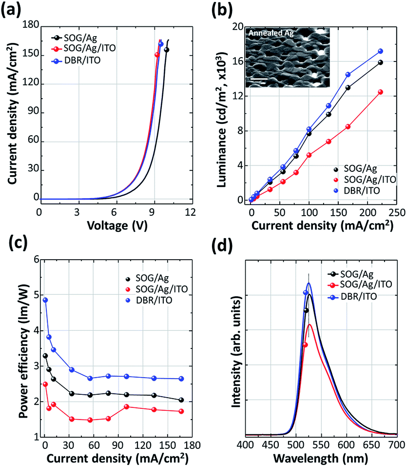 | ||
| Fig. 3 (a) Current density–voltage (J–V), (b) luminance–current density (L–J), (c) current density–power efficiency and (d) EL spectra characteristics of TOLEDs with three types of reflector/anode structures: Ag, Ag/ITO, and DBR/ITO. Inset: top-view of SEM image for 100 nm-Ag film annealed at 300 °C. | ||
Mechanical robustness is an important characteristic for the application of the metal foil substrate in flexible OLEDs. To investigate the operational stability of TOLEDs under mechanical bending stress, we measured the L–J–V characteristics with tensile bending strain (Fig. 4). Compared with the device without bending, the J–V characteristic of the device essentially showed no change with tensile bending strain (r = 5 cm, 0.5% tensile strain). For optical property, only 11% changes in maximum luminance were observed with the bending strain. When the bending radius decreased to 3 cm (0.8% strain), however, the operation voltage of the device drastically increased (ESI, Fig. S1†). It is known that the critical fracture strain for ZrO2 (0.5–0.8%) is smaller than that of other materials used for OLEDs (2.5% for SiO2, >1.4% for organic semiconductors).24,25 Thus, it is conceivable that repeated bendings at 0.5% strains induced cracks in the ZrO2 layer, resulting in a degradation of the devices. This situation can be improved by employing high index polymer film instead of ZrO2.
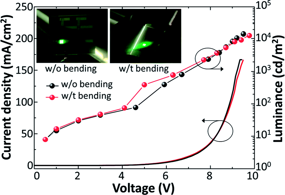 | ||
| Fig. 4 L–J–V characteristics of TOLEDs with DBR under mechanical bending strain (r = 5 cm). Inset: photographs of operating TOLEDs before and after the bending. | ||
Conclusions
In conclusion, high efficiency TOLEDs with a highly reflective DBR was demonstrated on a flexible steel foil substrate. We optimized the suitable multilayer structure of the DBR by optical simulation using the characteristic matrix method. Based on the theoretical simulation result, we deposited seven pairs of SiO2/ZrO2 by e-beam evaporation, and this DBR showed a high reflectance value of 90.5% at λ = 500 nm. The DBR served not only as the optical reflector, but also as the substrate insulating layer which enables electrical isolation and prevents crosstalk. The TOLEDs with DBR showed an operation voltage of 6.5 V at J = 10 mA cm−2 and a maximum luminance of 17400 cd m−2 at J = 225 mA cm−2. Furthermore, the electroluminescence property of TOLEDs was almost unchanged under a tensile bending condition (r = 5 cm). This work can be an innovative approach to overcome the reflective anode and substrate insulating difficulties for flexible TOLEDs on metal foil substrates. The aim of ongoing work is to investigate the possibility of using the microcavity effect to improve color purity and realize light magnification of flexible OLEDs. The driving voltage of the device can be reduced by incorporating functional buffer layers, e.g. hole injection layer, electron transport layer, and charge blocking layer.
Conflicts of interest
There are no conflicts to declare.Acknowledgements
This research was financially supported in part by the Basic Science Research Program through the National Research Foundation of Korea (NRF) funded by the Ministry of Education (NRF-2016R1D1A1B03932231).References
- J. Lee, K. An, P. Won, Y. Ka, H. Hwang, H. Moon, Y. Kwon, S. Hong, C. Kim, C. Lee and S. H. Ko, Nanoscale, 2017, 9, 1978–1985 RSC.
- L. Zhou, M. Yu, X. Chen, S. Nie, W.-Y. Lai, W. Su, Z. Cui and W. Huang, Adv. Funct. Mater., 2018, 28, 1705955 CrossRef.
- H.-H. Kuo, Y.-T. Chen, L. R. Devereux, C.-C. Wu, M. A. Fox, C.-Y. Kuei, Y. Chi and G.-H. Lee, Adv. Mater., 2017, 29, 1702464 CrossRef PubMed.
- A. Salehi, S. Ho, Y. Chen, C. Peng, H. Yersin and F. So, Adv. Opt. Mater., 2017, 5, 1700197 CrossRef.
- K. T. Ly, R.-W. Chen-Cheng, H.-W. Lin, Y.-J. Shiau, S.-H. Liu, P.-T. Chou, C.-S. Tsao, Y.-C. Huang and Y. Chi, Nat. Photonics, 2017, 11, 63–68 CrossRef.
- S. J. Lee, Y.-H. Kim, J. K. Kim, H. Baik, J. H. Park, J. Lee, J. Nam, J. H. Park, T.-W. Lee, R.-G. Yi and J. H. Cho, Nanoscale, 2014, 6, 11828–11834 RSC.
- T. Tsujimura, T. Hakii, T. Nakayama, H. Ishidai, T. Kinoshita, S. Furukawa, K. Yoshida and K. Osawa, J. Soc. Inf. Disp., 2016, 24, 262–269 CrossRef.
- H.-Y. Xiang, Y.-Q. Li, L. Zhou, H.-J. Xie, C. Li, Q.-D. Ou, L.-S. Chen, C.-S. Lee, S.-T. Lee and J.-X. Tang, ACS Nano, 2015, 9, 7553–7562 CrossRef PubMed.
- K.-H. Ok, J. Kim, S.-R. Park, Y. Kim, C.-J. Lee, S.-J. Hong, M.-G. Kwak, N. Kim, C. J. Han and J.-W. Kim, Sci. Rep., 2015, 5, 9464 CrossRef PubMed.
- R.-P. Xu, Y.-Q. Li and J.-X. Tang, J. Mater. Chem. C, 2016, 4, 9116–9142 RSC.
- J. K. Jeong, D. U. Jin, H. S. Shin, H. J. Lee, M. Kim, T. K. Ahn, J. Lee, Y. G. Mo and H. K. Chung, IEEE Electron Device Lett., 2007, 28, 389–391 Search PubMed.
- J. H. Cheon, J. H. Choi, J. H. Hur, J. Jang, S. S. Shin, J. K. Jeong, Y. G. Mo and H. K. Chung, IEEE Trans. Electron Devices, 2006, 53, 1273–1276 Search PubMed.
- Y. Choi, M. S. Park, J. H. Kwon and J. S. Gwag, J. Appl. Phys., 2012, 112, 074513 CrossRef.
- A. D. L. Bugallo, L. Rigutti, G. Jacopin, F. H. Julien, C. Durand, X. J. Chen, D. Salomon, J. Eymery and M. Tchernycheva, Appl. Phys. Lett., 2011, 98, 233107 CrossRef.
- S. H. Kim, J. H. Cheon, E. B. Kim, J. H. Bae, J. H. Hur and J. Jang, J. Non-Cryst. Solids, 2008, 354, 2529–2533 CrossRef.
- S. Chung, J.-H. Lee, J. Jeong, J.-J. Kim and Y. Hong, Appl. Phys. Lett., 2009, 94, 253302 CrossRef.
- Y.-F. Liu, J. Feng, D. Yin, Y.-G. Bi, J.-F. Song, Q.-D. Chen and H.-B. Sun, Opt. Lett., 2012, 37, 1796–1798 CrossRef PubMed.
- Y.-F. Liu, J. Feng, Y.-F. Zhang, H.-F. Cui, D. Yin, Y.-G. Bi, J.-F. Song, Q.-D. Chen and H.-B. Sun, Org. Electron., 2014, 15, 2661–2666 CrossRef.
- Y. Qu, C. Coburn, D. Fan and S. R. Forrest, ACS Photonics, 2017, 4, 363–368 CrossRef.
- F. Chi, L. Yan, H. Yan, B. Jiang, H. Lv and X. Yuan, Opt. Lett., 2012, 36, 1406 CrossRef PubMed.
- S. Kim, H. K. Yu, K. Hong, K. Kim, J. H. Son, I. Lee, K.-B. Kim, T.-Y. Kim and J.-L. Lee, Opt. Express, 2012, 20, 845–853 CrossRef PubMed.
- T. Mitsunari, T. Tanikawa, Y. Honda, M. Yamaguchi and H. Amano, J. Cryst. Growth, 2013, 370, 16–21 CrossRef.
- W. C. Tien, A. K. Chu, J. A. Lu, M. Y. Chang, M. J. Chuang, W. J. Zheng, C. M. Chao and W. Y. Huang, Org. Electron., 2012, 13, 2264–2271 CrossRef.
- M. Matsui, T. Soma and I. Oda, J. Am. Ceram. Soc., 1986, 69, 198–202 CrossRef.
- K. Hong, S. H. Kim, K. H. Lee and C. D. Frisbie, Adv. Mater., 2013, 25, 3413–3418 CrossRef PubMed.
Footnote |
| † Electronic supplementary information (ESI) available. See DOI: 10.1039/c8ra05759a |
| This journal is © The Royal Society of Chemistry 2018 |