
 Open Access Article
 This Open Access Article is licensed under a Creative Commons Attribution-Non Commercial 3.0 Unported Licence
Band offset and an ultra-fast response UV-VIS photodetector in γ-In2Se3/p-Si heterojunction heterostructures
Y. X. Fanga,
H. Zhanga,
F. Azadb,
S. P. Wangc,
F. C. C. Lingd and
S. C. Su *ad
*ad
aInstitute of Optoelectronic Material and Technology, South China Normal University, Guangzhou 510631, P. R. China. E-mail: shichensu@scnu.edu.cn
bSchool of Natural Sciences (SNS), National University of Sciences and Technology (NUST), H-12 Islamabad, Pakistan
cInstitute of Applied Physics and Materials Engineering, University of Macau, Macau 999078, China
dDepartment of Physics, The University of Hong Kong, Pokfulam Road, Hong Kong, People's Republic of China
First published on 21st August 2018
Abstract
High-quality γ-In2Se3 thin films and a γ-In2Se3/p-Si heterojunction were prepared using pulse laser deposition (PLD). The band offset of this heterojunction was studied by XPS and the band structure was found to be type II structure. The valence band offset (ΔEv) and the conduction band offset (ΔEc) of the heterojunction were determined to be 1.2 ± 0.1 eV and 0.27 ± 0.1 eV, respectively. The γ-In2Se3/p-Si heterojunction photodetector has high responsivity under UV to visible light illumination. The heterojunction exhibits highly stable photodetection characteristics with an ultrafast response/recovery time of 15/366 μs. The ultrafast response time was attributed to type II structure band alignment, which was good for the separation of electron–hole pairs and it can quickly reduce recombination. These excellent properties make γ-In2Se3/p-Si heterojunctions a promising candidate for photodetector applications.
1 Introduction
Two-dimensional layered semiconductors exhibit unique physical and chemical properties compared to their bulk counterparts. They have great application prospects in the field of nano-optoelectronic devices and have attracted widespread attention.1–4 However, stable high-performance of these two-dimensional layered semiconductor materials based devices has yet to be further explored. In the past decade, layered materials such as metal dichalcogenides (MoS2,5–7 MoSe2,8–10 WSe2,11–13 WS2 (ref. 14–17)), III–VI semiconductors (GaSe,18,19 GaS,20,21 InSe,22,23 In2Se3 (ref. 24 and 25)), V–VI semiconductors (Bi2Te3 (ref. 26 and 27)) and elemental semiconductors (black phosphorus28) have found useful applications in nanoelectronics and optoelectronics. Of the various chalcogenides, In2Se3 is an interesting III–VI n-type semiconductor due to its multiphase and excellent optical properties. It is also known to have at least five crystal forms (α, β, γ, δ and κ). At different temperatures with a specific stoichiometric ratio, different phases and crystal structures can coexist in case of In2Se3.24,29,30Generally, In2Se3 is a direct narrow bandgap semiconductor. Multilayered (ML) indium selenide exhibits high electron mobility, remarkable light absorption efficiency and sensitivity, and good stability which makes it one of the most promising materials for photodetection purposes. Because silicon is a general-purpose substrate for photovoltaic applications, combining In2Se3 with mature silicon technology has great potential for the preparation of photoelectric sensors with high detection performance. Current photodetection technology targets multi-spectral (wideband or dual-band) photodetectors for sensing, imaging under atmospheric conditions, object discrimination and optical communication applications.31
Up to now, various synthetic approaches have been used to prepare different In2Se3 heterostructures. Zhang et al. prepared the In2Se3/ZnO heterojunction and studied its offset structure.32 Chen et al. developed an effective colloidal process involving thermal injection to synthesize uniform nanoflowers consisting of 2D γ-In2Se3 nanosheets.33 Zheng et al. prepared a self-assembled broadband β-In2Se3/Si photodetector array for weak signal detection.34 Yang et al. Prepared the In2Se3/Pi nanosheets and studied its photoresponsivity.35 γ-In2Se3/Si has emerged as one of the most promising materials for visible photodetection due to its remarkable responsivity and detectivity in a wide range of wavelengths. In this work, a high-quality n type γ-In2Se3 thin film was successfully prepared by pulsed laser deposition (PLD). And we studied the valence band offset (ΔEv) and the conduction band offset (ΔEc) of the heterojunction.
The γ-In2Se3/p-Si heterojunction was prepared by depositing In2Se3 on p-Si substrate. The band offset of this heterojunction was studied by XPS. The γ-In2Se3/p-Si heterojunction exhibits significant responsivity and detectability over a wide range of wavelength. This heterojunction photodiode exhibits excellent response characteristics as an optoelectronic device.
2 Experimental
The In2Se3 was grown on Si substrate using the PLD method with solid targets of In2Se3 (99.99%). The deposition rate was calculated by using thickness of the grown films and deposition time and found to be 0.12 nm s−1. Background vacuum pressure was kept at 1 × 10⁻⁴ Pa. 248 nm pulsed line from a Coherent COMPexPro 102 excimer laser was used as laser source. The pulse energy and working frequency were maintained at 200 mJ and 2 Hz, respectively. The substrate temperature was kept at 600 °C during growth. At the end of growth, the samples were naturally cooled to room temperature and the sample was taken out to obtain In2Se3/p-Si heterojunction. X-ray photoelectron spectroscopy in this experiment was tested by the Kratos Axis Ultra XPS system. Al Kα (hν = 1486.6 eV) wavelength was used as an X-ray source which can accurately calibrate the work function and Fermi level.A typical XRD spectrum shown in Fig. 1 is a well-defined set of diffraction peaks for In2Se3. The XRD standard alignment card confirms that these peaks are assigned to the hexagonal phase of In2Se3 with lattice parameters: a = 0.71, c = 1.93 nm (JCPDS card, no. 71-0250) which means that it has a gamma phase structure.36 The Raman spectrum of gamma phase In2Se3 is shown in the inset of Fig. 1. It exhibits vibration mode at 123.8, 150.2, 173.9, and 241.0 cm−1, which are consistent with previously reported results.30The vibration mode at 302.0 cm−1 is consistent with reported of SiO2. The XRD pattern did not show any peak for impurity phases.
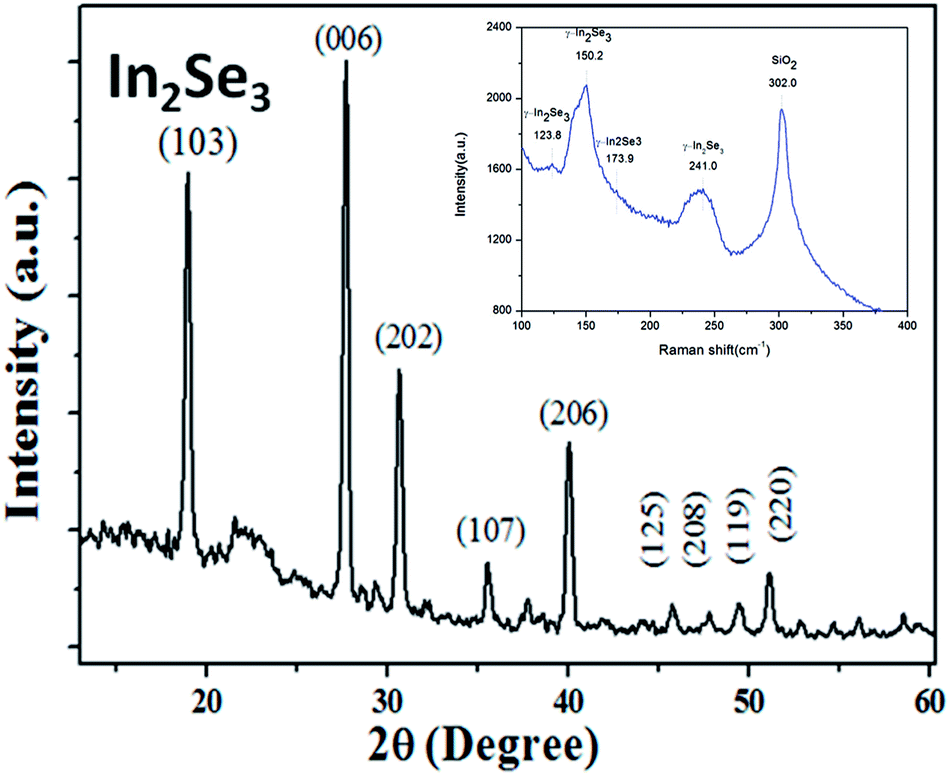 | ||
| Fig. 1 The XRD patterns and the Raman spectrum of the In2Se3. | ||
The characteristics of the band alignment of heterojunction is very important for the application of In2Se3/Si heterojunction as photodetector. There are many situations for which energy band structure diagram can be simulated by using the Anderson–Shockley model. However, in this paper, experimental methods are used to study the energy band offset of the In2Se3/Si heterojunction interface.
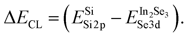
Fig. 2 shows Se3d core level peak from the top In2Se3 layer and Si2p core level peak originating from the underlying Si, and the difference in the core binding energy (ΔECL) for In2Se3/Si heterojunction. The valence band maximum (VBM) was determined by using linear extrapolation. The valence band offset (ΔEv) in terms of a binding energy difference ΔECL between core levels from each side of the interface is:
 | (1) |
 | (2) |
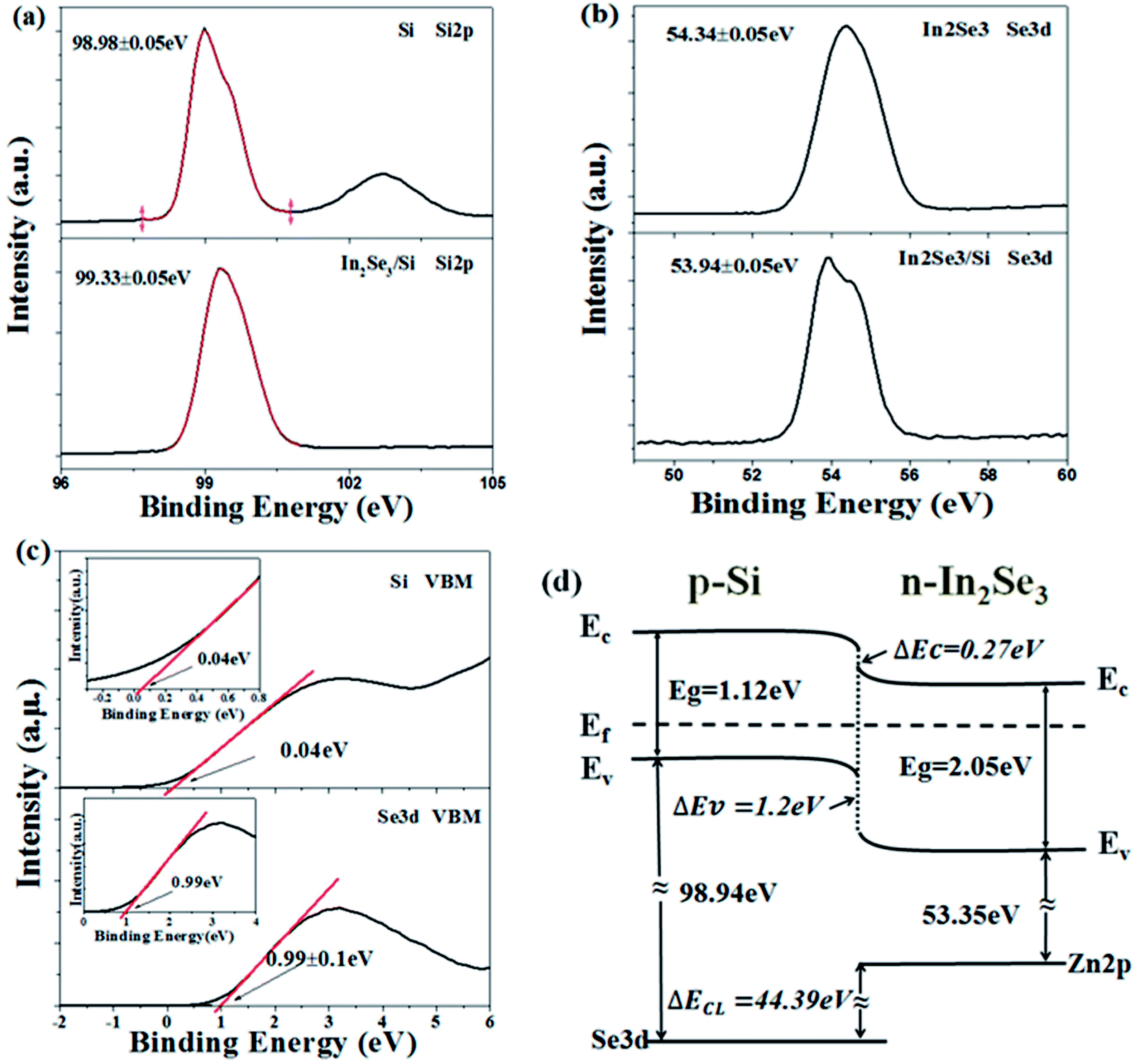 | ||
| Fig. 2 (a) The XPS CL spectra of the Zn2p state measured from the Si sample and In2Se3/Si heterojunction, (b) the XPS CL spectra of the Se3d state measured from the In2Se3 films and In2Se3/Si heterojunction, (c) the valence-band XPS spectrum of Si and In2Se3 films, and (d) energy band diagram of type-II band alignment of the In2Se3/Si heterojunction. | ||
The peak position of Si2p-core level in Si and In2Se3/Si found to be 98.98 ± 0.05 eV and 99.33 ± 0.05 eV, respectively (as shown in Fig. 2a). The CL of Se3d in In2Se3 was at 54.34 ± 0.05 eV, and in In2Se3/Si heterojunction at approximately 53.94 ± 0.05 eV (as shown in Fig. 2b). The valence band edge shown in Fig. 2c was used to measure the position of the VBM. The VBMs of Si and In2Se3 were determined to be 0.04 eV and 0.99 ± 0.1 eV, respectively. The Fig. 2c illustrates fitting of the low energy portion of the spectrum.
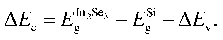
After the above data is substituted into eqn (1), the value of VBO (ΔEv) is calculated to be 1.2 eV. Since γ-In2Se3 is a direct bandgap semiconductor, the band gap of In2Se3 can be extrapolated to 2.05 eV.32 This is consistent with the previously reported data that band gap of layered γ-In2Se3 lies at 2–2.5 eV.37 As an indirect bandgap semiconductor, Si has a band gap of 1.12 eV at room temperature.
 | (3) |
Therefore, the conduction band offset (CBO) value is calculated to be −0.27 eV by eqn (3). The energy band diagram of γ-In2Se3/Si heterojunction is shown in Fig. 2d. Analyzing the band structure, it can be concluded that this heterojunction has a type II aligned structure.
The typical structure of γ-In2Se3/p-Si heterojunction photodetector is shown in the inset of Fig. 3. Fig. 3 shows a typical current–voltage (I–V) characteristic of different metal semiconductor contacts. The result shows that all the three contacts: Si–In2Se3, In–Si, Au–In2Se3 are Schottky contacts, the influence of contact between Au and In2Se3 and between In and Si can be neglected; the rectification behavior of this device mainly comes from the Schottky contact of the In2Se3/Si heterojunction. And the rectification ratio is calculated 76 from the figure. Therefore, the γ-In2Se3-ML/Si heterojunction appears to be a well-defined diode with a turn-on voltage of approximately 0.7 V.
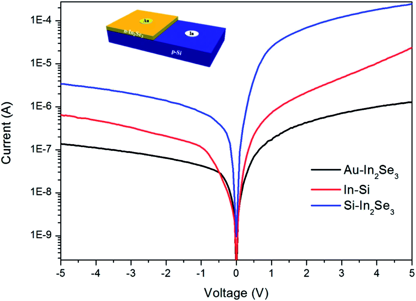 | ||
| Fig. 3 A typical plots of current voltage characteristics in different metal–semiconductor contacts and In2Se3/Si heterojunction. (Inset: schematic diagram of the γ-In2Se3-ML/Si heterojunction photodetector). | ||
Fig. 4a–d shows reverse biased portion of the I–V curve of γ-In2Se3/p-Si heterojunction in the dark, and at different light intensities using LED point light sources of 365, 420, and 500 nm for illumination (IK3301R-G). The reverse bias characteristics also confirms the rectifying behavior of the γ-In2Se3-ML/Si heterojunction. During forward bias condition, the current increases exponentially with voltage, whereas at larger reverse voltages, the increase in current tends to saturate. The reverse biased IV characteristics of γ-In2Se3/Si heterojunction in the dark and presence of light also confirms its photodiode behavior. As shown by the reverse biased I–V curves, the dark current is about −0.98 nA. Under the illumination of the LED spot light source, a notable increase in the current in the reverse biased region was observed. With three different light sources, the photoresponse was tested at different light intensities and wavelengths. Fig. 4d shows the strong photoresponse dependence on light intensity. The photocurrent increases significantly with increase in light intensity. These characteristics demonstrate high photosensitivity of the device under ultraviolet to visible light irradiation.
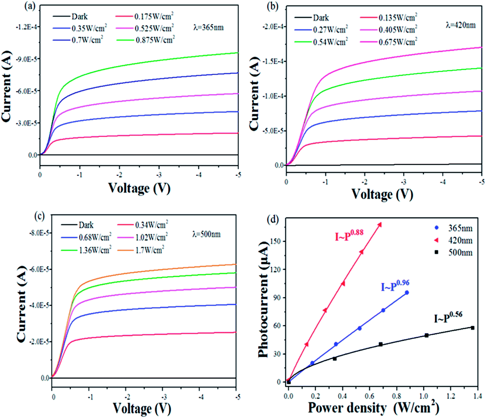 | ||
| Fig. 4 Photoelectric characteristics of In2Se3-ML/Si heterojunction in the dark, and their photoresponse at various wavelengths and different illumination intensities: (a) 360, (b) 420, and (c) 500 nm and; (d) photocurrent as a function of light intensity under the reverse bias voltage of −5 V. | ||
Using the power law function to fit the three curves in Fig. 4d, it was found that there is almost a linear relationship between the photocurrent and optical power density. The power law function: Iph = APα, where Iph stands for photocurrent (Iillumination − Idark); A is a constant at a specific wavelength; P is the power density of the incident light; and α is a power law index. The fitted curves show that α is 0.96, 0.86 and 0.56 for wavelengths of 365, 420 and 500 nm, respectively.
Since the heterojunction is formed by two materials with different lattice constants and lattice structures, the energy band at the interface is discontinuous and there are potential barriers and potential wells. Different lattice constants introduce defects and interface states heterojunction interface. First of all, at 500 nm, α is only 0.56. This sub-linear response is a result of complex process of electron–hole generation, trapping, and recombination in the semiconductors. At wavelengths of light of 365 and 420 nm, the alpha factor is close to the ideal state one, particularly at 365 nm, which indicates that the losses caused by recombination in the process of photoexcitation of carriers are relatively low. Both the trap states in In2Se3 and at the interface between In2Se3 and Si substrates may have recombination centers, which has also been confirmed in other photodetector materials.37,38 It can also be seen from Fig. 4d that the photocurrent increases more slowly as the light intensity increases at a wavelength of 365 nm as compared to 420 nm incident light at the bias voltage of −5 V. In contrast, the photocurrent from 420 nm light intensity increases faster.
The responsivity (Rres) is a useful figure-of-merit for a photodetector, which can be calculated from:
| Rres = Iph/IirrA | (4) |
The other important figure-of-merit is the external quantum efficiency (η), which can be calculated from:
| η = (Iph/e)/(IirrA/hν) | (5) |
The detectivity (D) can be calculated from:
| D = Rres/(2qJd)1/2 | (6) |
A time-resolved photo-response diagram under illumination of 365 nm light source with a reverse bias of −3 V is shown in Fig. 5a. Under the bias of −3 V, the current increases significantly from −1.5 μA (light off) to −192 μA (light on). Switch “on/off” ratio was found up to 128. The consistency of the seven switching cycles in Fig. 5a shows that the optical response has good stability and repeatability.
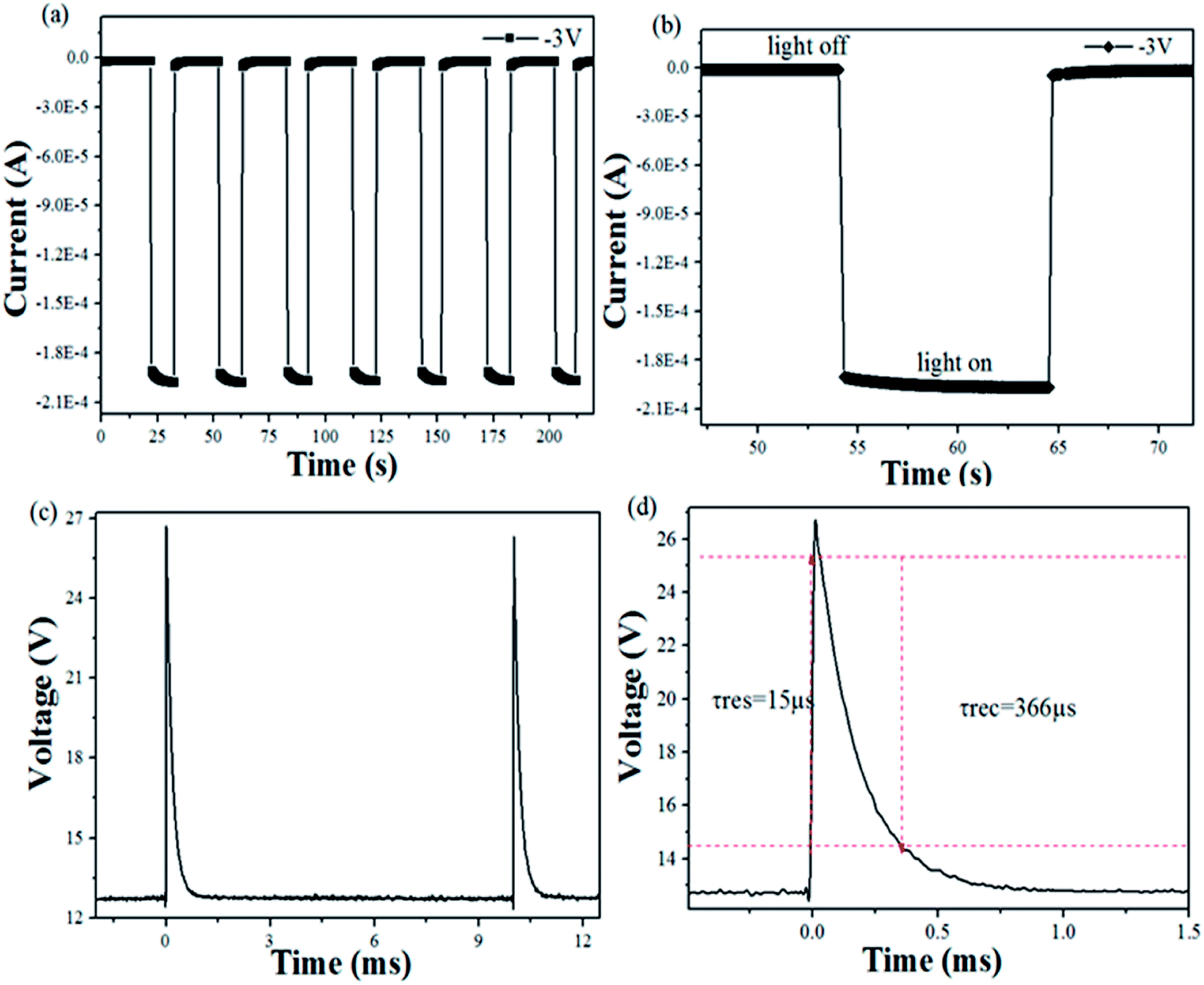 | ||
| Fig. 5 Optoelectronic performance of In2Se3-ML/Si heterojunction: (a) the seven-cycle time-resolved photoresponse under a bias of −3 V at 365 nm light illumination, (b) a single–period plot of the time-resolved photoresponse, (c) photoresponse of the photodetector at 266 nm laser by a Q-switch Nd:YAG and (d) photoresponse of single period in (c). | ||
Fig. 5c shows typical time response characteristics of γ-In2Se3/p-Si heterojunction photodiode. The response speed of the photodetector is usually characterized by the response time (τres)and the recovery time τrec. Whereas, response time is defined as the time required to increase 10% of its peak value to 90%, and the recovery time is the time taken to decay from 90% to 10% of its peak value. In order to extract an accurate response time, an enlarged response cycle is shown in Fig. 5d. The short response time (15 μs) and recovery time (366 μs) were observed in this work, which are much smaller than other heterojunction (such as α-In2Se3 (6 ms/12 ms), γ-In2Se3 (175 μs/226 μs), ZnO (104/-), MoS2 (31 μs/72 μs)).26,39,41,42 The ultrafast response attributed to II structure band alignment was good at the separation of electrons–hole pairs, and can fastly reduce their recombination.
3 Conclusions
In this paper, high quality γ-In2Se3/p-Si heterojunction were prepared using PLD. The band alignment of In2Se3/Si heterojunction was measured by XPS. The valence band offset (ΔEv) and the conduction band offset (ΔEc) of the heterojunction were determined to be 1.2 ± 0.1 eV and 0.27 ± 0.1 eV, respectively. Analysis of the band structure indicates that the γ-In2Se3/p-Si heterojunction has a type II band alignment structure. The γ-In2Se3/p-Si heterojunction photodiodes exhibit excellent rectification characteristics in the dark and at different incident optical powers, and have a broad spectral response ranging from UV to VIS with high responsivity and stability. And the ultrafast response time (15 μs) and recovery time (366 μs) indicate that the heterojunction has a fast response and detection performance.Conflicts of interest
There are no conflicts to declare.Acknowledgements
This work is supported by National Natural Science Foundation of China (Grant No. 61574063); Science and Technology Program of Guangdong Province, China (Grant No. 2017A050506047, 2017B030311013); Guangzhou Science and Technology Project (Grant No. 2016201604030047); Science and Technology Development Fund (FDCT 084/2016/A2) from Macau SAR; Multi-Year Research Grants (MYRG-00149-FST) from University of Macau.References
- K. S. Novoselov, et al., Two-dimensional atomic crystals, Proc. Natl. Acad. Sci. U. S. A., 2005, 102, 10451–10453, DOI:10.1073/pnas.0502848102.
- Q. H. Wang, K. Kalantar-Zadeh, A. Kis, J. N. Coleman and M. S. Strano, Electronics and optoelectronics of two-dimensional transition metal dichalcogenides, Nat. Nanotechnol., 2012, 7, 699–712, DOI:10.1038/nnano.2012.193.
- M. Shanmugam, R. Jacobsgedrim, E. S. Song and B. Yu, Two-dimensional layered semiconductor/graphene heterostructures for solar photovoltaic applications, Nanoscale, 2014, 6, 12682–12689 RSC.
- X. Duan, et al., Lateral epitaxial growth of two-dimensional layered semiconductor heterojunctions, Nat. Nanotechnol., 2014, 9, 1024 CrossRef PubMed.
- S. Yang, et al., Self-Driven Photodetector and Ambipolar Transistor in Atomically Thin GaTe-MoS2 p–n vdW Heterostructure, ACS Appl. Mater. Interfaces, 2016, 8, 2533–2539, DOI:10.1021/acsami.5b10001.
- H. Li, et al., Fabrication of single- and multilayer MoS2 film-based field-effect transistors for sensing NO at room temperature, Small, 2012, 8, 63–67, DOI:10.1002/smll.201101016.
- Z. Yin, et al., Single-layer MoS2 phototransistors, ACS Nano, 2012, 6, 74–80 CrossRef PubMed.
- C. Huang, et al., Lateral heterojunctions within monolayer MoSe2-WSe2 semiconductors, Nat. Mater., 2014, 13, 1096–1101, DOI:10.1038/nmat4064.
- D. Kong, et al., Synthesis of MoS2 and MoSe2 Films with Vertically Aligned Layers, Nano Lett., 2013, 13, 1341–1347 CrossRef PubMed.
- S. Larentis, B. Fallahazad and E. Tutuc, Field-effect transistors and intrinsic mobility in ultra-thin MoSe2 layers, Appl. Phys. Lett., 2012, 101, 193 CrossRef.
- Z. Zheng, et al., Flexible, transparent and ultra-broadband photodetector based on large-area WSe2 film for wearable devices, Nanotechnology, 2016, 27, 225501, DOI:10.1088/0957-4484/27/22/225501.
- W. Zhao, et al., Evolution of Electronic Structure in Atomically Thin Sheets of WS2 and WSe2, ACS Nano, 2013, 7, 791–797 CrossRef PubMed.
- W. Liu, et al., Role of Metal Contacts in Designing High-Performance Monolayer n-Type WSe2 Field Effect Transistors, Nano Lett., 2013, 13, 1983–1990 CrossRef PubMed.
- H. R. Gutierrez, et al., Extraordinary room-temperature photoluminescence in triangular WS2 monolayers, Nano Lett., 2013, 13, 3447–3454, DOI:10.1021/nl3026357.
- Y. Gong, et al., Vertical and in-plane heterostructures from WS2/MoS2 monolayers, Nat. Mater., 2014, 13, 1135–1142 CrossRef PubMed.
- T. Georgiou, et al., Vertical field-effect transistor based on graphene-WS2 heterostructures for flexible and transparent electronics, Nat. Nanotechnol., 2013, 8, 100–103 CrossRef PubMed.
- J. D. Yao and Z. Q. Zheng, et al., Stable, highly-responsive and broadband photodetection based on large-area multilayered WS2 films grown by pulsed-laser deposition, Nanoscale, 2015, 7, 14974, 10.1039/c5nr03361f.
- P. A. Hu, Z. Wen, L. Wang, P. Tan and K. Xiao, Synthesis of Few-Layer GaSe Nanosheets for High Performance Photodetectors, ACS Nano, 2012, 6, 5988 CrossRef PubMed.
- Y. Zhou, et al., Epitaxy and Photoresponse of Two-Dimensional GaSe Crystals on Flexible Transparent Mica Sheets, ACS Nano, 2014, 8, 1485 CrossRef PubMed.
- S. Yang, et al., High performance few-layer GaS photodetector and its unique photo-response in different gas environments, Nanoscale, 2014, 6, 2582–2587, 10.1039/c3nr05965k.
- P. Hu, et al., Highly responsive ultrathin GaS nanosheet photodetectors on rigid and flexible substrates, Nano Lett., 2013, 13, 1649–1654, DOI:10.1021/nl400107k.
- N. M. Gasanly, B. M. Yavadov, V. I. Tagirov and E. A. Vinogradov, Infrared and Raman Spectra of Layer InSe Single Crystals, Phys. Status Solidi B, 2010, 89, K43–K48 CrossRef.
- Z. Chen, J. Biscaras and A. Shukla, A high performance graphene/few-layer InSe photo-detector, Nanoscale, 2015, 7, 5981–5986 RSC.
- X. Tao and Y. Gu, Crystalline-crystalline phase transformation in two-dimensional In2Se3 thin layers, Nano Lett., 2013, 13, 3501–3505 CrossRef PubMed.
- J. Zhou, et al., Controlled Synthesis of High-Quality Monolayered α-In2Se3 via Physical Vapor Deposition, Nano Lett., 2015, 15, 6400–6405 CrossRef PubMed.
- J. D. Yao, et al., Polarization dependent photocurrent in the Bi2Te3 topological insulator film for multifunctional photodetection, Sci. Rep., 2015, 5, 14184 CrossRef PubMed.
- J. D. Yao and G. W. Yang, Flexible and High-Performance All-2D Photodetector for Wearable Devices, Small, 2018, 14, 1704524 CrossRef PubMed.
- X. Yu, S. Zhang, H. Zeng and Q. J. Wang, Lateral black phosphorene P–N junctions formed via chemical doping for high performance near-infrared photodetector, Nano Energy, 2016, 25, 34–41 CrossRef.
- Z. Zheng, J. Yao, J. Xiao and G. Yang, Synthesis of High-Quality Monolayered alpha-In2Se3 via Physical Vapor Deposition, Nano Lett., 2015, 15, 6400–6405, DOI:10.1021/acs.nanolett.5b01590.
- K. Kambas, C. Julien, M. Jouanne, A. Likforman and M. Guittard, Raman Spectra of α- and γ-In2Se3, Phys. Status Solidi B, 1984, 124, K105–K108 CrossRef.
- G. Ariyawansa, et al., Bias-selectable tricolor tunneling quantum dot infrared photodetector for atmospheric windows, Appl. Phys. Lett., 2008, 92, 111104 CrossRef.
- H. Zhang, S. S. Yan, S. T. Li and S. C. Su, Band alignment of In2Se3 multilayers/ZnO heterojunction measured by X-ray photoelectron spectroscopy, J. Mater. Sci.: Mater. Electron., 2018, 29, 6434–6438, DOI:10.1007/s10854-018-8624-0.
- S. Chen, et al., Facile Synthesis of gamma-In2 Se3 Nanoflowers toward High Performance Self-Powered Broadband gamma-In2 Se3/Si Heterojunction Photodiode, Small, 2017, 13 DOI:10.1002/smll.201604033.
- Z. Zheng, et al., Self-Assembly High-Performance UV-vis-NIR Broadband beta-In2Se3/Si Photodetector Array for Weak Signal Detection, ACS Appl. Mater. Interfaces, 2017, 9, 43830–43837, DOI:10.1021/acsami.7b16329.
- Z. Q. Zheng, J. D. Yao and G. W. Yang, Growth of centimeter-scale high-quality In2Se3 films for transparent, flexible and high performance photodetectors, J. Mater. Chem. C, 2016, 4(34), 8094–8103, 10.1039/c6tc02296k.
- A. Pfitzner and H. D. Lutz, Redetermination of the Crystal Structure of γ-In 2 Se 3 by Twin Crystal X-Ray Method, J. Solid State Chem., 1996, 124, 305–308 CrossRef.
- C.-H. Ho, Y.-C. Chen and C.-C. Pan, Structural phase transition and erasable optically memorized effect in layered γ-In2Se3 crystals, J. Appl. Phys., 2014, 115, 033501, DOI:10.1063/1.4862184.
- X. Zhou, et al., Ultrathin SnSe2 Flakes Grown by Chemical Vapor Deposition for High-Performance Photodetectors, Adv. Mater., 2015, 27, 8035–8041, DOI:10.1002/adma.201503873.
- S. Chen, et al., Facile Synthesis of γ-In2Se3 Nanoflowers toward High Performance Self-Powered Broadband γ-In2Se3/Si Heterojunction Photodiode, Small, 2017, 13, 1604033 CrossRef PubMed.
- Q. Hong, et al., Self-powered ultrafast broadband photodetector based on p–n heterojunctions of CuO/Si nanowire array, ACS Appl. Mater. Interfaces, 2014, 6, 20887–20894, DOI:10.1021/am5054338.
- K. C. Pradel, W. Jevasuwan and J. Suwardy, et al., Solution derived p-ZnO/n-Si nanowire heterojunctions for photodetection, Chem. Phys. Lett., 2016, 658, 158–161 CrossRef.
- J. Lu, J. H. Lu and H. Liu, et al., Improved photoelectrical properties of MoS2 films after laser micromachining, ACS Nano, 2014, 8, 6334–6343 CrossRef PubMed.
| This journal is © The Royal Society of Chemistry 2018 |