
 Open Access Article
 This Open Access Article is licensed under a Creative Commons Attribution-Non Commercial 3.0 Unported Licence
Light trapping and power conversion efficiency of P3HT![[thin space (1/6-em)]](https://www.rsc.org/images/entities/h2_char_2009.gif) :nano Si hybrid solar cells
:nano Si hybrid solar cells
Murugan Vinotha,
Sundaramoorthy Arunmethaa,
Mathu Sridharpandaya,
Subramani Karthika and
Venkatachalam Rajendran *ab
*ab
aCentre for Nano Science and Technology, K. S. Rangasamy College of Technology, Tiruchengode-637215, Tamil Nadu, India
bCentre for Nano Science and Technology, Dr. N. G. P. Arts and Science College, Dr. N. G. P. Kalapatti Road, Coimbatore-641048, Tamil Nadu, India. E-mail: veerajendran@gmail.com; vrajendran@drngpasc.ac.in
First published on 15th October 2018
Abstract
In this study, the hybrid solar cells (HSCs) were fabricated with high-purity nano Si from nano SiO2 precursor extracted from natural minerals, that is, quartz sand. The prepared nano Si was used as an electron transport material to prepare an active layer material mixture with poly(3-hexylthiophene) (P3HT) by mixing it in two composition ratios, namely 1![[thin space (1/6-em)]](https://www.rsc.org/images/entities/char_2009.gif) :1 and 1:0.8. The blended active layer solutions (ALSs) were prepared by using solvents such as 1,2-dichlorobenzene (DCB), chlorobenzene (CB), and chloroform (CF). The HSCs were fabricated using six blended ALSs, namely ALS1, ALS2, ALS3, ALS4, ALS5, and ALS6. The current density–voltage characteristics of the fabricated HSCs were studied using a simulated AM 1.5G illumination having light density power of 100 mW cm−2. The characterization properties such as short circuit current density (Jsc) and power conversion efficiency (PCE) were studied and compared with those of all six HSCs fabricated with six blended ALSs. At the outset, the P3HT:nano-Si (1:0.8) blended ALS in CB solvent shows 2.37% PCE, and 46% of external quantum efficiency (EQE) absorption which is higher than the other fabricated solar cells. This study discusses the possibilities of preparation of nano Si from natural mineral sand, as an effective electron transport material to fabricate HSCs with enhanced PCE.
:1 and 1:0.8. The blended active layer solutions (ALSs) were prepared by using solvents such as 1,2-dichlorobenzene (DCB), chlorobenzene (CB), and chloroform (CF). The HSCs were fabricated using six blended ALSs, namely ALS1, ALS2, ALS3, ALS4, ALS5, and ALS6. The current density–voltage characteristics of the fabricated HSCs were studied using a simulated AM 1.5G illumination having light density power of 100 mW cm−2. The characterization properties such as short circuit current density (Jsc) and power conversion efficiency (PCE) were studied and compared with those of all six HSCs fabricated with six blended ALSs. At the outset, the P3HT:nano-Si (1:0.8) blended ALS in CB solvent shows 2.37% PCE, and 46% of external quantum efficiency (EQE) absorption which is higher than the other fabricated solar cells. This study discusses the possibilities of preparation of nano Si from natural mineral sand, as an effective electron transport material to fabricate HSCs with enhanced PCE.
Introduction
Silicon solar cells are currently dominating the photovoltaic (PV) market, due to their high-power conversion efficiency (PCE), excellent charge transport properties, high purity, and environmental stability. Currently, the methods used to manufacture high-efficiency silicon wafer solar cells are expensive in terms of material preparation and fabrication. The possible alternative method to the fabrication of silicon wafer solar cells is bulk heterojunction (BHJ) polymer solar cells.1,2 Recently, preparation of bulk BHJ photovoltaic devices by different solutions has been reported using p-type conjugated polymers, in combination with n-type polymers3 or fullerenes.4 The main drawbacks of BHJ polymer solar cells are high hole mobility and low electron mobility. The intrinsic imbalances in carrier mobility and thermal stability present in BHJ polymer solar cells are overcome through HSCs based on a combination of polymer/organic/inorganic/nanocrystal (NC) materials.5–8The hybrid polymers and inorganic nanostructured materials are blended to form BHJ solar cells by considering the conducting properties of both type of materials such as solution processing of polymer semiconductors and high electron mobility of inorganic semiconductors. In an HSC, the active layer is formed by the direct interfacial connection between organic materials, such as small molecules and conducting polymers, and inorganic semiconductors such as Nc Si, TiO2, ZnO, PbS, CdSe, and CdS, as a nanostructured bilayered configuration.9–14 The inorganic electron acceptor material can provide more advantages to the system while maintaining a low fabrication cost and high electron mobility.
Although many studies devoted to applications of semiconductor nanocrystals in solar cells have been published,15–17 the improvement in the surface modification procedure and shell composition enhances the functionalities, such as charge transport and electron mobilities, of the solar cells. The physical origin of the impact of the surface modification procedure on charge separation, electron and hole mobilities process is still limited in BHJ solar cells. However, such an analysis provides a deeper insight into the elementary process occurring in the hybrid blends and, therefore, promotes the development of strategies to improve the PCE of an HSC.
In recent years, organic polymer as the donor material and inorganic semiconductor as the acceptor material are efficiently used to fabricate HSCs.18 The PCE of HSCs while using CdS,14 ZnO,11 and Si19 nanoparticles as an acceptor in HSCs are 2.17%,14 2%,11 and 1.06%,19 respectively. The nano Si shows low HOMO–LUMO level, which in turn enhances electron mobilities and PCE compared to other acceptor materials. The strategies such as deposition of donor and acceptor materials,20 substrate heating during deposition,21 ratio combinations,22 solubilization of small molecules to enable material blending via solution processing,23 and improvement of PCE are efficiently implemented.
In solution-processing method, solvents are mainly shown with a packed chain of donor and acceptor materials through blending.23 Photoactive layer solvents are used to improve the optical absorption, morphology and electron mobility. The choice of solvent on a photoactive layer increases its tuning absorption and the interface spectral region of the HSC.18,24 The exciton of electron in acceptor material in the HSC is limited due to its percentage weight ratio and hence, its affects the generation of photocurrent density.18 The current density of the HSC generally depends on the weight ratio of acceptor material. Although limited studies are carried out on the selection of solvent and solution concentration, a comprehensive knowledge on the performance of the HSC device is essentially required.
Nano Si-based HSCs are intensively studied due to their unique advantages such as easy fabrication, high electron mobility, and higher efficiency compared with traditional solar cells.24,25 In our recent study, cost-effective fabrication of HSC with high-purity nano Si as an acceptor material revealed the PCE to be 1.06%.19 The magnesiothermic reduction process19 for preparing nano Si is a chemical-free and cost-effective method in which a natural raw material (quartz sand) is used.26,27 The quartz sand, which contains high amounts of silicon dioxide, is the most useful source to prepare high-purity silicon for solar cell applications.19,27 The magnesiothermic reduction process is one of the best conversion methods to obtain silicon from silicon dioxide with enhanced purity without changing the original morphology.28 The use of nano Si in the HSC opens up a new dimension in research to increase its light-trapping ability, that is, tunable absorption and PCE.
In this study, we aimed to produce nanostructured Si particles from quartz sand by magnesiothermic reduction reaction technique. The bilayered HSC solar cells were fabricated with ITO/PEDOT:PSS/P3HT:nano-Si/Al configuration. The blended (ALS) of P3HT:nano Si with two composition ratios, namely 1:1 and 1:0.8, were prepared using three organic solvents, namely 1,2-dichlorobenzene (DCB), chlorobenzene (CB), and chloroform (CF). The characterization properties such as PCE and tunable absorption were explored and compared among the various HSCs fabricated using two active-layer composition blends in three solvents.
Materials and methods
Nano Si from quartz sand
Quartz sand was collected from southern part of Indian Peninsula (i.e., Tuticorin, Tamil Nadu, India). The collected sand was washed with 50 ml of 10% HCl for 2 h to remove the metal ions. The leached quartz sand was filtrated and washed with double-distilled (DD) water, and then dried at 100 °C. The dried residue and sodium hydroxide pellets were mixed in a ratio of 1:1 and then fused at 400 °C for 3 h. The fused mixture was leached with DD water. The obtained mixture was filtered and then titrated with 10 N of H2SO4 to get a gel. The obtained gel was washed with DD water several times and then dried at 200 °C for 8 h in a hot-air oven to attain silica particles. The obtained silica particles were blended with Mg powder in a ratio of 1:1 using high-energy ball mill (PM100; Resteh, Germany) without losing their structure. Further, the mixture was heated at 600 °C at a rate of 10 °C min−1 for up to 4 h in Ar (95 vol%)/H2 (5 vol%) atmosphere. The heat-treated mixture was immersed in 1 M of HCl solution for 5 h and then immersed in a 10 wt% HF solution for 10 min. The obtained mixture was vacuum-dried at 100 °C for 3 h, to get the nanostructured Si particles.
Active layer solution
The HSC structure consists of an active layer sandwiched between a transparent indium tin oxide (ITO) anode and metal cathode aluminum (Al), as shown in Fig. 1. The active layer was prepared by mixing P3HT (poly(3-hexylthiophene)) and nano Si powders in two ratios, namely 1:1 and 1:0.8. The powders were dissolved in three different solvents, namely DCB, CB, and CF. Initially, P3HT (regioregularity of 96.6%; Ossila Ltd.) (25 mg ml−1) and nano Si (25 mg ml−1) powders at a stoichiometric ratio of 1:1 were dissolved in the DCB solvent separately. The dissolved solution was stirred for 5 h at 50 °C in N2 atmosphere inside a glove box to avoid unwanted molecule formation in the solution. The dissolved solutions were mixed and stirred for 12 h at 50 °C inside the glove box. The obtained blended active-layer solution was termed as ALS1. Then, the solution was spun-coated onto quartz substrate surface to record ultraviolet-visible (UV-Vis) absorption of ALS1. A similar procedure was used to get uniform P3HT:nano-Si blended ALS in solvents CB and CF, termed as ALS2 and ALS3, respectively. The above experimental procedure was repeated to prepare the uniformly blended ALS with P3HT (25 mg ml−1) and nano-Si (20 mg ml−1) powders in 1:0.8 ratio in the three solvents. The obtained blended ALS in solvents DCB, CB, and CF were termed as ALS4, ALS5, and ALS6, respectively.
 | ||
| Fig. 1 Basic Structure of HSC. | ||
Device fabrication
Using nano Si obtained from quartz sand, the HSCs were fabricated employing four steps. In step 1, the ITO-coated substrate with a sheet resistance of ∼10 Ω cm−2 was cut into 12.5 cm × 12.5 cm plates. These plates were first cleaned sequentially with DD water, acetone, and isopropyl in an ultrasonic bath for 10 min each. The cleaned plates were dried in N2 gas and subsequently placed under vacuum treated with oxygen (O2) plasma for 10 min with 150 W power. This resulted in an increased porosity and hydrophilic nature of the coating surface. In step 2, the poly(3,4-ethylenedioxythiophene)/poly(styrenesulfonate) (PEDOT:PSS; Aldrich) solution was initially filtered through a 0.45 μm filter.The filtered solution was spun-coated (∼40 nm thickness) onto the surface of the ITO at 3000 rpm for 60 s. Then, the substrate was heat-treated at 150 °C for 10 min in N2 atmosphere to obtain uniform coating. Step 3 involved the coating of the prepared active layer solution on the surface of the prepared PEDOT:PSS. The blended active layer solution, that is, ALS1 was initially filtered through a 0.45 μm filter. Then, the filtered solution was spun onto the PEDOT:PSS surface at 1000 rpm for 50 s and left to baking at 120 °C. Step 4 included the process of completion of fabrication of the HSC device. An aluminum layer (∼100 nm) was coated on the top surface of the active layer to provide contacts by using a vacuum evaporator (∼10−5 mbar) through a shadow mask and monitoring its thickness (SQM-310). The fabricated HSC device with an active area of 0.045 cm2 was termed as D1. Similar procedures were used to fabricate the HSC devices, namely D2, D3, D4, D5, and D6, by using the blended active layer solutions, namely ALS2, ALS3, ALS4, ALS5, and ALS6.
Characterization
The structures of the prepared nano SiO2 and Si particles were analyzed through an X-ray diffractometer (XRD; X'Pert PRO; PANalytical, he Netherlands). The XRD patterns were obtained using CuKα as a radiation source (λ = 1.54060 Å) with an applied constant current and voltage 30 mA and 40 kV, respectively, at a scan range of 10–80°. The particle size distribution measurement was carried out with a submicrometer particle size analyzer (Nanophox; Sympatec, Zellerfeld, Germany) using dynamic light-scattering technique. The average particle size d90 (i.e. d90, average diameter of 90 particles) of the nano SiO2 and Si particles were measured at a scattering angle of 90°.The samples were characterized by an X-ray photoelectron spectroscope (XPS, PHOIBOS HSA3500; SPECS, Germany) to reveal the chemical composition and the relative concentration of nano Si particles. The XPS spectra were recorded using a (VG Microtech) at a base pressure ∼10−10 mbar. The XPS setup used in this study was incorporated with a dual-anode Mg–Al X-ray source with a hemispherical analyzer and a Channeltron detector with a resolution of 1.3 eV.
The morphology, microstructure, and composition of the prepared nano SiO2 and nano Si particles were measured using a field emission scanning electron microscope (FESEM, Ultra 55; Zeiss, Gemini, Australia) coupled with energy-dispersive spectroscopy (EDS).
The absorption spectra of the nano Si particles were obtained using a UV-Vis spectrometer (Cary 8454; Agilent, Singapore) over a wide range (180–800 nm) at a step size of 5 Å. Thereafter, 0.1 mg nano Si was dispersed in ethanol and then transferred to a 2 ml cuvette for UV-Vis analysis. The bandgap energy (Eg) of the nano Si particles was obtained using the following equation:
 | (1) |
During the J–V characterization in forward bias measurement, the ITO electrode was used as a positive electrode whereas the coated Al was used as a negative electrode. The J–V characteristics of all the fabricated HSC devices were studied with a computer-controlled source meter (2400 SourceMeter; Keithley) along with a solar simulator (CT 100 AAA; Oriel Sol3A, Newport Corporation) with an AM 1.5G spectral correction filter with 100 mW cm−2 light intensity.
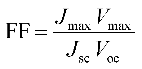
The fill factor (FF) and the overall incident light power to electrical power conversion efficiency of the solar cell was calculated using the following equations:
 | (2) |
 | (3) |
Results and discussion
The XRD patterns for nano SiO2 and Si particles are shown in Fig. 2. The observed hump in the XRD pattern in the 2θ range from 15 to 30 indicates the disorder structure of nano SiO2, due to its amorphous nature.29 The XRD pattern for the nano Si reveals its crystalline nature. The major peaks observed at θ = 28, 47, 56, 69, and 76 correspond to the planes (111), (220), (311), (400), and (331), respectively. The average crystallite size measured from the full-width at half maximum of the corresponding peaks using the Scherrer formula30 was 54 nm. All the peaks revealed the formation of face-centered cubic structure of Si (JCPDs file no. 27-1402, 1999), which is more suitable for energy conversion applications.31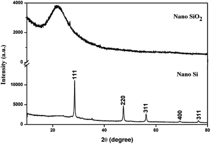 | ||
| Fig. 2 XRD pattern of nano SiO2 and nano Si. | ||
Fig. 3 shows the particle size distribution of nano SiO2 and Si particles. The particle size distribution for nano SiO2 shows a broad range distribution, that is, in the range of 8–79 nm. The average particle size of nano SiO2 (i.e., d90) is 26 nm. After magnesiothermic reduction process, a larger shift in particle size distribution of the obtained nano Si particles was observed. A narrow particle size distribution in the range of 5–47 nm was noticed in nano Si compared with nano SiO2 particles. The average particle size distribution for nano Si was 15 nm.
 | ||
| Fig. 3 PSD of nano SiO2 and nano Si. | ||
The FESEM image and EDS pattern for the nano SiO2 particles are shown in Fig. 4a. The FESEM image of nano SiO2 particles (Fig. 4a(i)) clearly indicates that the particles are agglomerated and have spherical morphology. The EDS pattern shows the presence of silicon and oxygen atoms, and also confirms the formation of nano SiO2 particles. Fig. 4a(ii) shows that the elemental composition oxygen-to-silicon ratio in nano SiO2 is 64:36. The surface morphology of nano Si shown in the SEM image in Fig. 4b(i) illustrates its spherical morphology with the absence of interfacial gaps. The absence of interfacial gaps helps to enhance the conductivity32 of the nano Si particles. The elemental composition of nano Si is 92%, as shown in Fig. 4b(ii). The structures of nano Si and SiO2 are same due to modified magnesiothermic reduction process.
 | ||
| Fig. 4 FESEM images of (a) nano SiO2 and (b) nano Si. | ||
The XPS measurement shows the high purity of the prepared nano Si particles. As shown in Fig. 5a, two main peaks, Si2p and Si2s, are observed. The binding energy of nano Si at Si2p and Si2s is 99.0 and 154 eV, respectively (Fig. 5b and c). The peak position of Si2p exhibits a stronger and higher energy region of Si. The weak peak observed at 103 eV shows the existence of a small amount of amorphous SiO2, as reported earlier.33 In contrast, the Si2p spectrum of completely reduced silicon nanoparticle formed by using the modified magnesiothermic reduction process contains mainly a peak for Si–Si bonds at 99 eV. The high purity of nano Si particles shows that they can be used in electronic and energy conversion applications.34
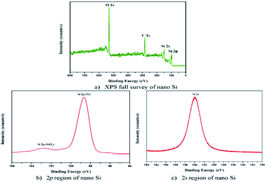 | ||
| Fig. 5 XPS binding energy of nano Si particles (a) Full survey of nano Si, (b) 2p region of nano Si and (c) 2s region of nano Si. | ||
The UV-Vis absorption spectra for the nano Si are shown in Fig. 6. The absorption takes place at 480 nm in the visible region. The energy bandgap is obtained using the following relation:
| αhv = A(hv − Eg)n/2 | (4) |
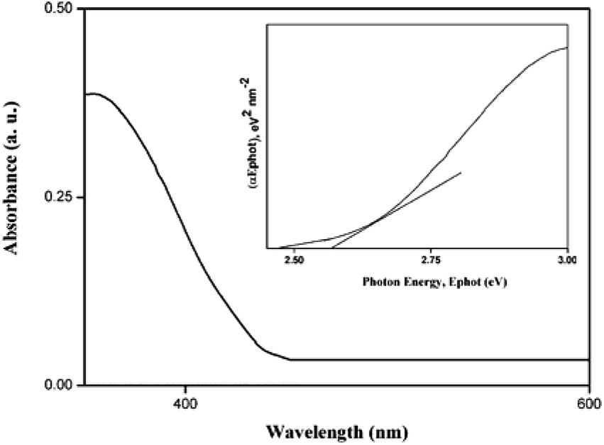 | ||
| Fig. 6 UV-Visible absorption for nano Si and inset photon energy. | ||
The absorption spectra of P3HT:nano-Si active layer in two weight ratios (1:1 and 1:0.8) blended in three solvents after coating on quartz substrate are shown in Fig. 7. The absorption spectra for the P3HT:nano-Si (1:1) active layer in ALS1 (DCB), ALS2 (CB), and ALS3 (CF) solvents are shown in Fig. 7. In all three solvents, the absorption peak is observed in UV-Vis spectra region between 300 and 550 nm. The absorption spectrum for P3HT:nano Si active layer in CF (ALS3) solvent shows a weak absorbance in the range of 300–550 nm due to absence of a conjugated double bond of the solvent.36 The existence of polymer–solvent disorder in the ALS may strongly lead to reduction in the absorption intensity. A high peak intensity is observed in ALS2 with CB as a solvent at 350 and 550 nm with relatively high interactions of chain molecules in the active layer materials.37 A small but noticeable intensity peak is observed in ALS1 in DCB solvent, which shows the presence of λmax with a conjugated double bond.38 The DCB solvent shows higher absorption intensity peak compare with other two solvents (CB and CF), which supports photon excitons and electron transfer between donor and electrode. The absorption spectra for P3HT:nano Si active layer with 1:0.8 ratio in three solvents, that is, ALS4 (DCB), ALS5 (CB), and ALS6 (CF), are shown in Fig. 7.
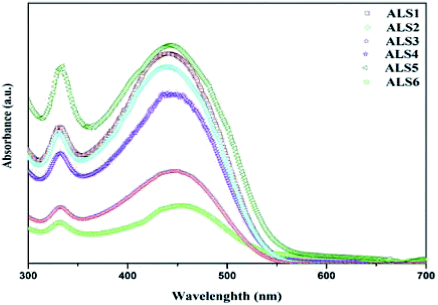 | ||
| Fig. 7 Effect of UV absorption on different ratios and solvents. | ||
ALS6 shows a broad absorption peak with low intensity between 350 and 550 nm, which affects the interaction between donor and acceptor in active layer. ALS4 shows a higher intensity peak at 350 and 550 nm in DCB solvent. The observed peak can be attributed to the (π–π*) transitions of the ALS4 active layer.39,40 ALS5 in CB solvent shows higher absorption than ALS4 and ALS6, which in turn helps to enhance the generation of exciton and interaction of molecules. The knowledge on the UV-Vis absorption spectra of the active layer is key to fabricate the polymer HSC with higher conductivity pathways, improved hole and electron mobility using different stoichiometric compositions of active layer materials and solvents. Among all six ALSs, a significant enhancement in the UV-Vis absorption spectra for ALS1 (DCB solvent, 1:1) and ALS5 (CB solvent, 1:0.8) can be noticed from Fig. 7. The observed higher absorption intensity in DCB (ALS1) and CB (ALS5) solvents may attribute to enhanced photon harvesting and hence leads to higher exciton generation. This in turn reflects on Jsc, which depends on the absorption coefficient of the active layer, the exciton-dissociation rate, and electron transport property.24 The magnitude of the absorption of P3HT:nano Si blends improved the light harvesting from visible region. The obtained higher Jsc and PCE by improving the optical absorption in the visible region, dissociation of excitons, and the electron transport then already reported standard HSCs.25,41
The nanoscale morphology of P3HT:nano Si thin films is studied using tapping-mode AFM. Variation in the surface morphology and RMS surface roughness of P3HT:nano Si active layer in three different solvents and two different ratios (1:1 and 1:0.8) coated in thin films as shown in Fig. 8. The 1:1 ratio of DCB(ALS1) solvent coated film reveals a smooth surface with rms roughness of 2.33 nm.42 On the other hand, CB(ALS2) and CF(ALS3) solvents coated films shows higher surface roughness with rms values of 2.73 nm and 3.24 nm respectively. The ratio of 1:0.8 coated film revealed better distribution and diffusion of P3HT with nano Si matrix. The rms value for the DCB(ALS4), CB(ALS5) and CF(ALS6) solvent coated films is respectively 2.04 nm, 1.64 nm, and 2.89 nm. This variation in the surface roughness appears to have significant effect on the performance of devices. In general, ALS5 coated thin film reveals less rms value leading to an enhanced light absorption and the number of exciton generation.42 The distribution of active layer in ALS5 coated thin film may also facilitate the electron transportation as well as better diffusion results in good interpenetrating network which in turn supports to improved the performance solar cell.43
 | ||
| Fig. 8 AFM images of P3HT:nano Si thin films on tapping mode: (a) ALS1, (b) ALS2, (c) ALS3, (d) ALS4, (e) ALS5 and (f) ALS6. | ||
The current voltage characteristics (Jsc–Voc) of the fabricated HSC devices D1, D2, and D3 using the ALS1, ALS2, and ALS3, respectively, are shown in Fig. 9a. However, the Jsc–Voc characteristics of HSC devices, namely D4, D5, and D6, fabricated using ALS4, ALS5, and ALS6, respectively, are shown in Fig. 9b. A comprehensive analysis of Jsc–Voc characteristics of all the fabricated HSC devices helps in exploring the electron and hole mobility between P3HT and nano Si, as reported earlier.44,45 The current–voltage characteristics parameters, namely Jsc, Voc, FF, and PCE for all HSC devices are shown in Table 1. In any chosen active layer composition, that is, 1:1 or 1:0.8, the solvent is changed to explore the electron and hole mobility between P3HT and nano Si. The FESEM images of the fabricated architecture ITO (120 nm)/PEDOT:PSS (60 nm)/P3HT:nano-Si (160 nm)/Al (100 nm) for D5 are shown in Fig. 10. It can be seen that the overall active layer thickness remains constant and indicates a well-defined interaction between molecules in P3HT:nano Si in D5, as reported earlier.23
 | ||
| Fig. 9 Jsc–Voc characteristics of fabricated devices by using different ratio in different solvent. | ||
:nano Si active layer in different weight ratios and solvents
| Device name | Characteristics parameters | Jsc (calc.), (mA cm−2) | |||
|---|---|---|---|---|---|
| Jsc (mA cm−2) | Voc (V) | FF | PCE% | ||
P3HT:nano Si (1![[thin space (1/6-em)]](https://www.rsc.org/images/entities/b_char_2009.gif) :1) :1) |
|||||
| D1 | 9.84 | 0.49 | 0.43 | 2.12 | 9.45 |
| D2 | 8.86 | 0.45 | 0.42 | 1.71 | 8.23 |
| D3 | 6.13 | 0.39 | 0.41 | 0.97 | 5.84 |
|
|||||
| P3HT:nano Si (1:0.8) |
|||||
| D4 | 9.98 | 0.47 | 0.44 | 2.06 | 9.53 |
| D5 | 11.02 | 0.52 | 0.41 | 2.37 | 10.75 |
| D6 | 7.44 | 0.44 | 0.38 | 1.26 | 6.67 |
 | ||
| Fig. 10 FESEM of fabricated architecture of HSC. | ||
The Jsc and Voc of D1 show higher values than D3 whereas for D2, they lie in between. Further, the PCE of D1 is 75% higher than D2 (Table 1), which is ascribed to enhanced molecular interactions and electron transitions. The enhanced PCE is ascribed to absorption coefficient of the solvent and conjugated double bond as evident from UV-Vis results (Fig. 7). Similarly, the PCE of D1 is 40% higher than that of D2. The observed higher Jsc values for D1 (9.84 mA cm−2) than D2 (8.86 mA cm−2) and D3 (6.13 mA cm−2) reveal the enhanced electron mobility of nano Si used as an acceptor material. The above studies confirm that ALS1 in DCB solvent leads to generation of more excitons, which in turn separates the electron hole pairs of HSCs.44 Therefore, the interaction between P3HT:nano-Si ALSs in DCB solvent is higher than that of solvents CB and CF, resulting in an increased intermolecular excitons, as reported earlier.19,20,27
The current–voltage characteristics of D4 and D6 reveal similar behaviors as those of D1 and D2, whereas the current–voltage characteristics of D5 reveal a different behavior. The observed higher magnitude of Jsc for D5 in CB solvent can be due to the enhanced UV-Vis absorption of ALS5. This results in enhanced generation of photon excitons in the ALS5 and hence, may lead to a 2.37% increase in PCE (Table 1). The observed increase for D5 is due to improved absorption in ALS5s, as noticed from the spectra shown in Fig. 7. The PCE of the device D5 is two times higher than that of HSC obtained using nano Si (1.06%).19 The observed higher Voc value (0.52) in D5 than that in D1, D2, D3, D4, and D6 indicates an improvement in the energy level between the valence and conduction bands of the active layer, as reported earlier.24 The observed higher PCE (2.37%) in D5 is due to higher level of excitons of HOMO–LUMO. In case of D1, the possibility of HOMO–LUMO level is less because of the lower recombination rate resulting in lower Jsc (9.84 mA cm−2) of D1 than D5 (11.02 mA cm−2).46 The above observation shows that D5 fabricated with P3HT:nano-Si in the ratio 1:0.8 in CB solvent exhibits higher PCE (2.37%) than the previously reported PCE (1.06%).19 This clearly shows that the HSC can be fabricated using nano Si as a potential active material with enhanced PCE.
Fig. 11 shows a comparision of the EQE spectra of fabricated all six hybrid solar cells with different active layer. The higher absorption wavelengths ranging from 400 nm to 600 nm. The maximum EQE is 46% at 530 nm obtained by the device D5 with active layer ASL5 (CB solvent) this difference is due to the complex index of refraction of the active layer.47
 | ||
| Fig. 11 EQE spectra for fabricated HSCs using different ratio in different solvent. | ||
Conclusion
High-purity nano Si was extracted from natural mineral (quartz sand) by magnesiothermic reduction reaction method. The prepared nano Si was used as an acceptor material for the fabrication of HSC devices. The active layer with a mixture of materials P3HT and nano-Si in the ratios 1:1 and 1:0.8 was taken to obtain ALSs using solvents DCB, CB, and CF. The absorption spectra for all six ALSs reveal that ALS1 (DCB) and ALS5 (CB) show higher magnitude of absorption. Six HSC devices (i.e., D1, D2, D3, D4, D5, and D6) were fabricated using the prepared ALSs such as ALS1, ASL2, ALS3, ALS4, ALS5, and ALS6, respectively. Among six fabricated HSC devices, the PCE of ALS5 coated D5 (2.37%) is 11.79% higher than ALS1 coated device D1 (2.12%) and also exhibits better performance. Our best results, in this work are achieved 2.37% of PCE, 11.02 mA cm−2 of Jsc and 46% of EQE in a ratio of 1:0.8 in CB solvent devices its enhanced absorption coefficient and electron mobility while compare with other solvent devices. The EQE results higher absorption in this study reveals the possibilities of preparation of nano Si from natural mineral sand as an effective acceptor material to fabricate HSCs with enhanced PCE.
Conflicts of interest
Authors have no conflicts to declare.Acknowledgements
Authors are thankful to SERB, DST, New Delhi, India for their financial supports (File No. EMR/2014/000311) to carryout this project. The authors also acknowledge the support and efforts for the characterization, fabrication and testing of HSCs devices was carried out at the Center of Excellence in Nanoelectronics (CEN), Indian Institute of Technology (IIT), Bombay, under the Indian Nanoelectronics users' program.References
- S. Günes, H. Neugebauer and N. S. Sariciftci, Chem. Rev., 2007, 107, 1324–1338 CrossRef PubMed.
- G. Li, R. Zhu and Y. Yang, Nat. Photonics, 2012, 6, 153–161 CrossRef CAS.
- G. Li, V. Shrotriya, J. Huang, Y. Yao, T. Moriarty, K. Emery and Y. Yang, Nat. Mater., 2005, 4, 864–868 CrossRef CAS.
- J. P. Thomas and K. T. Leung, Adv. Funct. Mater., 2014, 24, 4978–4985 CrossRef CAS.
- Y. Zhou, M. Eck and M. Kruger, Energy Environ. Sci., 2010, 3, 1851–1864 RSC.
- T. Xu and Q. Qiao, Energy Environ. Sci., 2011, 4, 2700–2720 RSC.
- S. Thiyagu, T.-C. Lin, H.-J. Syu, C.-F. Lin, C.-C. Hsueh and C.-T. Liu, RSC Adv., 2015, 5, 13224–13233 RSC.
- X. Shen, B. Ma, L. Chen and J. Zhao, RSC Adv., 2017, 7, 688–693 RSC.
- C.-Y. Liu, Z. C. Holman and U. R. Kortshagen, Adv. Funct. Mater., 2010, 20, 2157–2164 CrossRef CAS.
- C. Y. Kuo, W. C. Tang, C. Gau, T. F. Guo and D. Z. Jeng, Appl. Phys. Lett., 2008, 93, 033303–033307 CrossRef.
- S. D. Oosterhout, M. M. Wienk, S. S. van Bavel, R. Thiedmann, L. Jan Anton Koster, J. Gilot, J. Loos, V. Schmidt and R. A. J. Janssen, Nat. Mater., 2009, 8, 818–824 CrossRef CAS PubMed.
- S. Gunes, K. P. Fritz, H. Neugebauer, N. S. Sariciftci, S. Kumar and G. D. Scholes, Sol. Energy Mater. Sol. Cells, 2007, 91, 420–423 CrossRef.
- N. Radychev, I. Lokteva, F. Witt, J. Kolny-Olesiak, H. Borchert and J. Parisi, J. Phys. Chem. C, 2011, 155, 14111–14122 CrossRef.
- S. Dowland, T. Lutz, A. Ward, S. P. King, A. Sudlow, M. S. Hill, K. C. Molloy and S. A. Haque, Adv. Mater., 2011, 23, 2739–2744 CrossRef CAS PubMed.
- S.-C. Shiu, J.-J. Chao, S.-C. Hung, C.-L. Yeh and C.-F. Lin, Chem. Mater., 2010, 22, 3108–3113 CrossRef CAS.
- S. Avasthi, S. Lee, Y. L. Loo and J. C. Sturm, Adv. Mater., 2011, 23, 5762–5766 CrossRef CAS PubMed.
- W.-C. Kwak, T. G. Kim, W. Lee, S.-H. Han and Y.-M. Sung, J. Phys. Chem. C, 2009, 113, 1615–1619 CrossRef CAS.
- I. Gonzalez-Valls and M. Lira-Cantu, Energy Environ. Sci., 2009, 2, 19–34 RSC.
- S. Arunmetha, M. Vinoth, S. R. Srither, A. Karthik, M. Sridharpanday, R. Suriyaprabha, P. Manivasakan and V. Rajendran, J. Electron. Mater., 2017, 47, 493–502 CrossRef.
- W. J. E. Beek, M. M. Wienk and R. A. J. Janssen, Adv. Mater., 2004, 16, 1009–1013 CrossRef CAS.
- O. Oklobia and T. S. Shafai, Solid-State Electron., 2013, 87, 64–68 CrossRef CAS.
- G. Wei, S. wang, K. Renshaw, M. E. Thompson and S. R. Forrest, ACS Nano, 2010, 4, 1927–1934 CrossRef CAS PubMed.
- J. G. Van Dijken, M. D. Fleischauer and M. J. Brett, Org. Electron., 2011, 12, 2111–2119 CrossRef CAS.
- C.-Y. Liu, Z. C. Holman and U. R. Kortshagen, Adv. Funct. Mater., 2010, 20, 2157–2164 CrossRef CAS.
- S.-H. Tsai, H.-C. Chang, H.-H. Wang, S.-Y. Chen, C.-A. Lin, S.-A. Chen, Y.-L. Chueh and J.-H. He, ACS Nano, 2011, 5, 9501–9510 CrossRef CAS PubMed.
- T. Nohira, K. Yasuda and Y. Ito, Nat. Mater., 2003, 2, 397–401 CrossRef CAS PubMed.
- W. Wang, J. C. Martin, R. Huang, W. Huang, A. Liu, A. Han and L. Sun, RSC Adv., 2012, 2, 9036 RSC.
- D. P. Wong, R. Suriyaprabha, R. Yuvakumar, V. Rajendran, Y.-T. Chen, B.-J. Hwang, L.-C. Chen and K.-H. Chen, J. Mater. Chem. A, 2014, 2, 13437–13441 RSC.
- S. Arunmetha, A. Karthik, S. R. Srither, M. Vinoth, R. Suriyaprabha, P. Manivasakan and V. Rajendran, RSC Adv., 2015, 5, 47390–47397 RSC.
- S. Karthik, P. Siva, K. S. Balu, R. Suriyaprabha, V. Rajendran and M. Maaza, Adv. Powder Technol., 2017, 28, 3184–3194 CrossRef CAS.
- R. Cisneros, H. Pfeiffer and C. Wang, Nanoscale Res. Lett., 2010, 5, 686–691 CrossRef CAS PubMed.
- S. Kemaloglu, G. Ozkoc and A. Aytac, Thermochim. Acta, 2010, 499, 40–47 CrossRef CAS.
- S. R. Bywalez, H. Karacuban, H. Nienhaus, C. Schulz and H. Wiggers, Nanoscale Res. Lett., 2012, 7, 76 CrossRef PubMed.
- D. S. Jensen, S. S. Kanyal, N. Madaan, M. A. Vail, A. E. Dadson, M. H. Engelhard and M. R. Linford, Surf. Sci. Spectra, 2013, 20, 36 CrossRef.
- D. Arun kumar, J. Merline Shyla and F. P. Xavier, Appl. Nanosci., 2012, 2, 429–436 CrossRef CAS.
- L. S. Hund and C. H. Chen, Mater. Sci. Eng., R, 2002, 39, 143–222 CrossRef.
- S.-Y. Chuang, H.-L. Chen, W.-H. Lee, Y.-C. Hunang, W.-F. Su, W.-M. Jen and C.-W. Chen, J. Mater. Chem., 2009, 19, 5554–5560 RSC.
- Y. B. Tiwari, S. Sharma and N. Bala, International Journal of Plastic and Polymer Technology, 2013, 3, 1–8 Search PubMed.
- W. J. E. Beek, M. M. Wienk and R. A. J. Janssen, Adv. Funct. Mater., 2006, 16, 1112 CrossRef CAS.
- S. L. W. Ji, W. S. Shih, T. H. Fang, C. Z. Wu, S. M. Peng and T. H. Meen, J. Mater. Sci., 2010, 45, 3266–3269 CrossRef.
- S. S. Li¢ and W. Robert Thurber, Solid-State Electron., 1977, 20, 609–616 CrossRef.
- S. Kundua and T. L. Kelly, Mater. Chem. Front., 2017, 2, 81–89 RSC.
- W. J. E. Beek, M. M. Wienk, M. Kamerink, X. Yang and R. A. J. Janseen, J. Phys. Chem. B, 2005, 109, 9505–9516 CrossRef CAS PubMed.
- D. Herrmann, S. Niesar, C. Scharsich, A. Kohler, M. Stutzmann and E. Riedle, J. Am. Chem. Soc., 2011, 133, 18220–18233 CrossRef CAS PubMed.
- J. Derr, K. Dunn, D. Riabinina, F. Martin, M. Chaker and F. Rosei, Physica E, 2009, 41, 668–670 CrossRef CAS.
- M. Wright and A. Uddin, Sol. Energy Mater. Sol. Cells, 2012, 107, 87–111 CrossRef CAS.
- L. A. A. Pettersson, L. S. Roman and O. Inganas, Appl. Phys. Lett., 1999, 86, 487 CAS.
| This journal is © The Royal Society of Chemistry 2018 |