
 Open Access Article
 This Open Access Article is licensed under a Creative Commons Attribution-Non Commercial 3.0 Unported Licence
Growth and properties of ZnO nanorods by RF-sputtering for detection of toxic gases†
Camilla Baratto
CNR-INO & University of Brescia, Sensor Lab, Via Branze 45, Brescia, Italy. E-mail: camilla.baratto@ino.it
First published on 14th September 2018
Abstract
There is a strong demand for nanostructured materials prepared by an industrially-scalable technique. The current work is devoted to the preparation of ZnO polycrystalline nanorods using RF sputtering at 400 °C and Sn droplets as a catalyzer layer, for highly sensitive gas sensors. Nanorods with diameters ranging from 100 to 200 nm can be tailored by changing the RF power and the deposition time. Raman and PL spectroscopy indicate that the material obtained is ZnO, with a characteristic emission spectrum in the UV region and in the visible. The functional properties of the ZnO nanorods were investigated by studying the response to CBRN (acetonitrile and DMMP), explosive (H2), and pollutant gases (H2S, acetone, and NO2) in the temperature range 200–500 °C. The sensors showed good response to reducing gases at higher temperatures (500 °C) and to NO2 at lower temperature (200 °C).
A Introduction
Nanoscale semiconductors with controlled morphology and structure are thoroughly investigated due to their promising potential applications in the fabrication of novel functional devices. Among nanostructured materials, one dimensional (1D) metal oxides have received enormous attention due to their high surface to volume ratio, that can be exploited to enhance surface reactions and gas adsorption.ZnO is a wide band gap semiconductor (Eg = 3.37 eV), with high exciton binging energy (60 meV), that shows interesting optical properties at room temperature.1,2 ZnO has been investigated for applications in light emitting diodes (LED),3–5 dye sensitized solar cells,6 biosensors,7 and piezoelectric nanogenerators.8
For gas sensing application, ZnO is one of the most interesting oxide that was used both for conductometric and optical transduction sensors.9,10 Detection principle is based on the interaction of gas molecules with ionized oxygen species of O−, O2− that are on the surface of ZnO in ambient air at a temperature in the range 250–500 °C. The reaction of a reducing gases with the ionized oxygen, releases an electron into the conduction band of ZnO, thus increasing carrier number. For conductometric sensors, the variation is observed by reading an increase in the current.11
ZnO 1D materials are usually synthesized as single crystalline nanowires by vapour phase growth technique12 and hydrothermal growth,13 while they are prepared as polycrystalline nanorods by plasma enhanced chemical vapour deposition (PECVD),14 electrochemical anodization15 and RF-sputtering.16–18
Among the cited techniques, sputtering deposition is a well-known, cost effective technology that can be used in large scale plants. Despite this, there are in literature few works that deal with ZnO nanorods prepared by sputtering: ZnO nanorods were grown at low temperature starting from rough Cu layer,16 Ga doped ZnO buffer layer,17 of FTO (Fluorine Tin Oxide) thin film.18 We recently demonstrated that ZnO nanorods were obtained by RF sputtering on magnetic Co/Sn layer:19 in this case the use of relatively low temperature during growth, allowed to maintain the magnetic properties of the Co layer.
To date, no extensive investigation is present on the growth of ZnO nanorods using a Sn catalyzer. The current paper aims to investigate the growth parameters of ZnO nanorods with Sn catalyzer on an insulating substrate (alumina), and to correlate the physical and morphological properties of the material with its functional properties. Among different gases that can be detected by ZnO gas sensor,20–22 the current work focuses on dangerous or poisonous gases: H2 is an explosive gas produced in industrial reactions, Dimethyl Methyl Phosphonate (DMMP) is a simulant of sarin nerve agent (concentration around ppm), NO2 is an air-pollutant, H2S is toxic and bad tolerated due to rotten-egg smell, acetonitrile is a simulant for hydrogen cyanide compounds.
B Experimental
Nanorods preparation by RF sputtering
ZnO nanorods were deposited by RF magnetron sputtering system onto 3 × 3 mm2 Al2O3 substrates. A seed layer of Sn was deposited from Sn target, maintaining the substrate at 400 °C: since the temperature is higher than Sn melting point, it grows as droplets on the alumina substrate. The droplets act as the catalyst for the subsequent growth of the ZnO nanorods. High pressure deposition (10−2 mbar) induced columnar growth resulting into ZnO nanorods. The RF power was varied from 100 to 150 W, while the deposition time was varied from 10 to 15 minutes, as resumed for clarity in Table 1 along with samples' names. The conformation of the obtained layer was very porous due to nanorods formation. The thickness was not measurable with conventional method like profilometer, yet a thicker layer of rods is expected for longer deposition times.| Sample name | Deposition power (W) | Deposition time (min) |
|---|---|---|
| ZNOS10 | 100 | 10 |
| ZNOS11 | 100 | 15 |
| ZNOS12 | 150 | 10 |
| ZNOS13 | 150 | 15 |
For functional tests with gases, Pt interdigitated electrodes and heater were deposited by RF magnetron sputtering. A Pt meander was deposited on the back-side of the substrate to provide heating by Joule effect. Before the tests, the sensing layers were aged on the TO-5 case by heating the sensors at 500 °C in ambient air for two weeks.
Electron microscopy characterization
The samples' morphology was investigated by scanning electron microscopy (SEM, Zeiss LEO 1525) in conventional mode (recording the secondary electrons with an InLens detector) with an accelerating voltage of 10 kV.Raman and photoluminescence spectroscopy
Photoluminescence (PL) and Raman spectra were collected using a modular micro-Raman confocal system from Horiba, equipped with a single monochromator and a Peltier-cooled charge-coupled device camera. A solid state laser at 325 nm (PL)/442 nm (Raman) wavelength was used as the excitation source, along with interference filters on the laser lines and edge filters on the signal. For Raman spectroscopy, a 100× objective and 1800 l mm−1 grating were used. For PL spectroscopy, a 40× UV objective and 600 l mm−1 grating were used.Functional characterization
Sensing tests were performed in a stainless steel test chamber (1000 cm3) at an ambient temperature of 20 °C, at atmospheric pressure, using a constant flux (300 cm3 min−1) with 30% relative humidity (RH). Gas species (acetone, DMMP, acetonitrile, H2, H2S, NO2) were diluted in dry air and contained in certified bottles. A constant bias (1 V direct-current) was applied to the sensing film and the electrical current was measured by a picoammeter (Keithley model 486).Sensor were tested at constant temperature [300 °C–400 °C–500 °C]. Relative response towards reducing gases (sensor response, R) was calculated as R = (IF − I0)/I0, where IF is the steady state current in gas and I0 is the steady state current in air. Relative response towards oxidizing gases was calculated as R = (I0 − IF)/I0. Response (recovery) times were calculated as the time needed to reach 90% (70%) steady state value in gas (air). Due to the physical constraint of the test chamber (flow 300 cm3 min−1 – and volume 1000 cm3) a complete exchange of the chamber atmosphere takes more than three minutes, so shorter response and recovery times cannot be evaluated in the present setup.
C Results and discussion
The morphology of the as-grown ZnO layer was characterized by SEM. Since the previous literature on ZnO nanorods showed that there is growth at room temperature from porous copper layer,17 Cu catalyzer deposited by sputtering was firstly tested; because of low porosity of Cu layer, no directional growth of ZnO was observed – Fig. 1(a).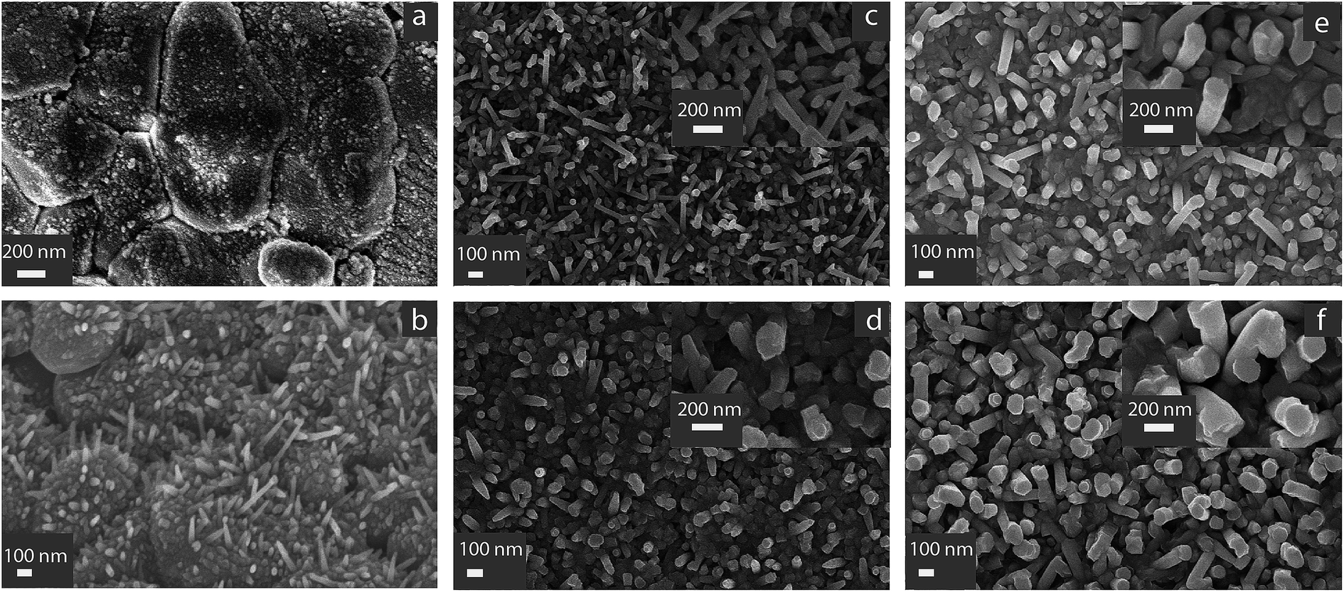 | ||
| Fig. 1 (a) Morphology of ZnO thin film deposited on Cu catalyzer: no nanorods formation can be observed. (b) High magnification images of early growth stage for ZNOS10 acquired with the sample tilted at 30°; (c–f) top view of ZnO nanorods obtained by different deposition conditions, along with high magnification image in the inset: (c) 100 W, 10 min (ZNOS10); (e) 100 W, 15 min (ZNOS11); (d) 150 W, 10 min (ZNOS12); (f) 150 W, 15 minutes (ZNOS13). | ||
Growth from FTO thin film at temperatures higher than 400 °C was reported in ref. 16 the authors postulated that the locally presence of SnO on FTO surface decomposed at the deposition temperature (400 °C) and the decomposed metallic Sn reacts with the sputtered Zn to form the liquid phase. The liquid droplets formed on FTO surface act as nucleation sites for ZnO nanorods during sputtering. Taking inspiration from the mechanism involving the liquid phase between Sn and ZnO at temperatures higher than 370 °C (Sn melting point), in the present work we used Sn as the starting seed.
The procedure followed was similar to that used to prepare SnO2 thin films sensors by RGTO (Reothaxial Growth and Thermal Oxidation) technique: in that case a Sn layer is deposited at 400 °C for about 2 minutes, resulting in droplet growth because substrate temperature is higher than 370 °C,23 followed by oxidation in oven. For ZnO nanorods formation, the need of much smaller tin droplets than those used for SnO2 RGTO thin films, suggested to use very short deposition time (5 s). We experimentally determined that increasing the deposition time of Sn to 10 s and 15 s Sn resulted in the growth of a continuous ZnO film without nanorods development (not shown). Fig. 1(b) shows early growth stages of the sample deposited at 100 W. The alumina substrate is covered by spherical agglomerates with dimension ranging around 50 nm; in some regions tapered nanorods are observable. The nanorods growth direction is randomized with respect to the vertical to the substrate.
As shown in Fig. 1(c) the thinnest rods were obtained by the lowest RF sputtering power (100 W) and 10 minutes deposition (Fig. 1(c)). In this case the diameter of the rod is around 80–100 nm as can be observed in the inset at higher magnification. Some rods are tapered towards the tip to a smaller diameter. Several rods have the longer axes tilted with respect to the normal to the substrate.
The diameter of the rod increased to 150 nm by increasing the deposition time to 15 minutes (Fig. 1(e)). When the deposition power increase to 150 W, the rod diameter increases to 140 nm for 10 minutes deposition – Fig. 1(d) – and 190 nm for 15 minutes deposition – Fig. 1(f). In case of Fig. 1(d), the presence of a compact layer between rods can also be observed at the bottom.
For 150 W deposition power, the rods are also more aligned along the vertical to the substrate, with respect to the 100 W condition.
Micro-Raman and micro-photoluminescence spectroscopy
The Raman spectroscopy was used to characterize the crystalline phase of the sensors (Fig. 2). Since the sensing material was deposited on an alumina substrate, the signal from alumina was also reported, as acquired from the substrate. A1(TO) mode of the substrate at 418 cm−1 was used for spectra normalization.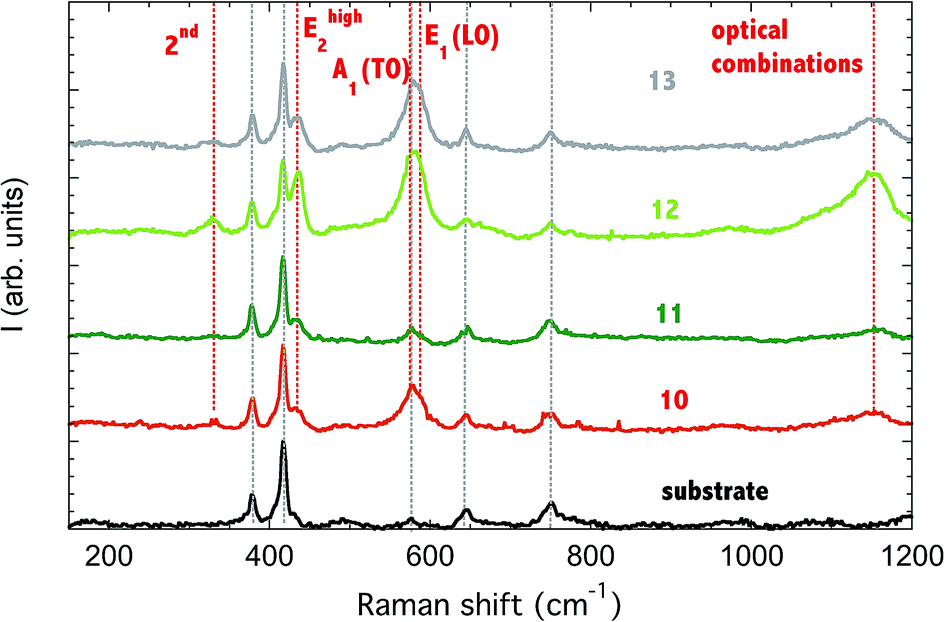 | ||
| Fig. 2 Raman spectra of ZnO nanorods sensors deposited on alumina substrate, compared to the substrate signal. Gray dotted lines correspond to substrate vibrations, red dotted lines to ZnO vibrations. | ||
All deposited ZnO nanorods showed the ZnO signature, namely the Ehigh2 mode at 436 cm−1 (437 cm−1 in ref. 24), E1 (LO) at 583 cm−1, the 2nd order multi-phonon combination of (Ehigh2–Elow2) at 328 cm−1 and the second order band at 1152 cm−1, due to optical combinations. A1(TO) mode at 574 cm−1 can also be observed, superposed to the substrate mode, with higher intensity for samples ZNO10, ZNO12 and ZNO13.
The Elow1 mode is outside the measurement range (99 cm−1). A1(TO) mode at 380 cm−1 is hidden by a substrate mode.
The samples ZNO12 and ZNOS13 shows higher intensity of ZnO vibrations if compared to the substrate signal. This is an indirect evidence that a thicker layer of nanorods is obtained at 150 W.
Photoluminescence spectroscopy allows to characterize the emission properties of ZnO nanorods. ZnO has a strong emission spectrum at room temperature, dominated by near-band-edge (NBE) emission in the UV range (around 380 nm) attributed to excitonic emission. Depending on the preparation condition, a broad band in the visible range can be observed from green to red, due to the presence of deep levels distributed in the band gap region. The origin of visible emission in ZnO nws is still debated: the defect involved could be a single ionized oxygen vacancy,25 an antisite oxygen,26 donor–acceptor complexes or interstitial Zn.27 The spectra in Fig. 3 shows typical NBE emission with a peak in the UV range and broad emission from 500 to 700 nm. The peak observed around 760 nm is the second order of the NBE peak.
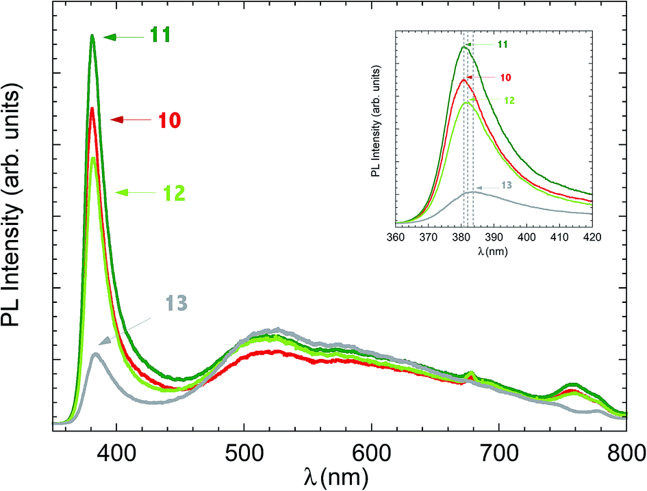 | ||
| Fig. 3 PL spectra of ZnO nanorods sensors acquired at room temperature. The ratio of the NBE emission over defect emission is considered a measure of the crystalline quality of the ZnO. (Inset) Detail of NBE emission: a blue shift in the peak position can be observed going from sample ZNOS13 to ZNOS10. Dotted lines are merely a guide for the eye. | ||
A close-up on NBE peak is presented in the inset of Fig. 3. The NBE peak position shifts from blue to red (380.8–381.3–381.5–383.8 nm)-going from sample ZNOS10 to ZNOS13, and this can be considered as an indication of the increased diameter of the nanorods,28 in agreement with SEM images (Fig. 1).
The ratio of the NBE to deep level emission (DLE) peak, measured under constant laser power conditions, can be used as an index of the quality of the nanostructures:29 in the present case it is higher for samples deposited at lower power (ZNOS10 and ZNOS11) and decreases for the samples deposited at 150 W (ZNOS12 and ZNOS13).
Gas sensing tests
The gas sensing tests were carried out to test the performances of ZnO nanorods as gas sensors and to test the influence of sample morphology on the sensing properties. The working temperature was varied from 200–500 °C by a 100 °C steps.Fig. 4 shows response to NO2 (1–1.5–2 ppm) for the best performing sensor ZnOS12. NO2 behave as an oxidizing gas, inducing a decrease in the current when the temperature ranged from 200 °C to 400 °C. The noise observed at 400 °C is due to a disturbance during the measurements. Response and recovery times at 200 and 300 °C are of the order of minutes, while they decrease at 400 °C at the expense of sensor response. At 500 °C no detection of NO2 was observed.
 | ||
| Fig. 4 Dynamic curves for sensor ZNOS12 when NO2 (1–1.5–2 ppm) was introduced. Gas carried wad humid air (30%) at room temperature. | ||
Hydrogen is an explosive gas, thus detection at concentration much below the Lower Explosion Limit (LEL, equal to 4%) is very important. The range of concentrations analysed here was [50–300 ppm]. Fig. 5(a) shows the sensing behaviour of the ZnO sensors towards H2 at 400°C: the analysis of the dynamic current variation, demonstrated a complete recovery of the baseline. ZnOS11 was the best performing sensor. ZNOS11 and ZNOS13 showed increased response and recovery times with respect to ZNOS11 and ZNOS12. Referring to SEM image (Fig. 1), we can observe that the slower sensors are the one with bigger nanorods – Fig. 1(e) and (f).
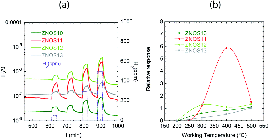 | ||
| Fig. 5 (a) Dynamic curve of the tested sensors at 400 °C towards 50–100–200 and 300 ppm of H2; (b) relative response to 100 ppm of H2 at different temperatures for all sensors; the lines between experimental point are a guide for the eyes. | ||
Fig. 5(b) reports the sensing behaviour of all sensors with H2 in the analysed temperature range. ZnO based sensors showed good relative responses to H2 at 400 and 500 °C. At 300 °C a detection was evident, but the sensor dynamic was too slow (not shown).
Fig. 6(a–d) shows relative responses of the tested sensors to low concentrations of H2S (3–5–7 ppm) from 300 °C to 500 °C. H2S behave as a reducing gas: an increase in sensor current was observed for ZnO based sensors. ZnO nanorods were sensible to H2S presence even at 300 °C but the relative response washigher at 500 °C. Response and recovery times decreased from 300 °C to 500 °C, being of the order few minutes at 500 °C.
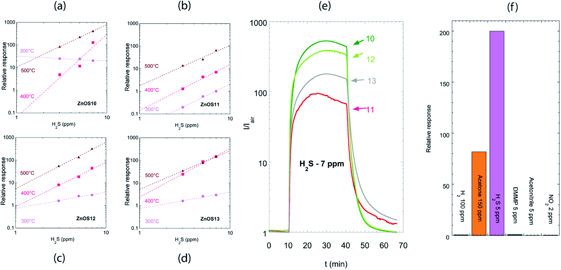 | ||
| Fig. 6 Relative response to 3–5–7 ppm of H2S in the temperature range [300 °C–500 °C] for (a) ZNOS10, (b) ZNOS11, (c) ZNOS12, (d) ZNOS13; the dotted line are the fit of the data with a power law. (e) Dynamic curve of sensors at 500 °C towards 7 ppm of H2S. (f) Selectivity to 6 gases measured for ZnOS10 sensor at 500 °C. | ||
The better sensors for H2S are ZNOS10 and ZNOS12, working at 500 °C; the data in Fig. 6(a) and (c) were fitted by a power law response = A × [concentration]B. Extrapolation of data fit to axis limit (ESI, see Fig. S1†) showed that the limit of detection for ZNOS10 is 0.1 ppm, while for ZNOS12 is 0.2 ppm.
At 500 °C the dynamic curves for the two sensors were comparable – Fig. 6(e) – while the worse response was observed for ZnOS11. ZNOS11 and ZNOS13 showed also slower recovery of the baseline value: these sensors were the ones with bigger rods diameter.
ZnO nanorods prepared by RF sputtering have performances much better compared to those obtained with ZnO single crystalline nanowires,30 being ΔR/R = 0.25 to 5 ppm for sensor analyzed in the reference, while in our case ΔR/R = 200 to the same concentration for ZNOS10 sensor.
There is debate in literature on the mechanism responsible for H2S detection with ZnO. Chen et al.31 claimed that the high sensing capabilities of 20–50 nm diameter ZnO nanowires to ppm level H2S was due to sulfuration reaction when H2S was introduced into test chamber. Instead, the reaction scheme usually associated with the detection of reducing gases in metal oxide semiconductors, takes into account the reaction of H2S with oxygen ionosorbed over the surface, with a consequent release of electrons into the conduction band.32 In the present work, the latter mechanism is more probable due to higher dimension of the nanorods used, and to the higher working temperature used. Moreover, in the conventional sensing mechanism, the calibration curve was described by a power law, while in the case of sulfuration reaction the calibration curve was fitted with a line.31
Fig. 6(f) shows the comparison of the sensor response towards six different species: five reducing gases (H2, acetone, H2S, DMMP and acetonitrile), and one oxidizing gas (NO2). At 500 °C, response to H2S is two orders of magnitude higher than response to H2 and DMMP (0.8 and 1 respectively), and three orders of magnitude higher than response to NO2 and to acetonitrile (0.3 and 0.2 respectively). The response is only one order of magnitude higher than the response to acetone, for which indeed the concentration is much higher (150 ppm versus 5 ppm).
We can thus observe partial selectivity towards H2S at 500 °C. At lower temperatures (200 °C), no response to reducing gases is observed, thus the sensors are partially selective to NO2 in this temperature range. A feasible approach to lower the cross-sensitivity of ZnO material in view of the sensor application, is the use of one ZnO sensor working at 500 °C and another ZnO sensor working at 200 °C in an array configuration: higher selectivity can be gained using pattern recognition.33
D Conclusions
In summary, ZnO polycrystalline nanorods was easily prepared by RF sputtering, starting from Sn catalyzer. The diameter of ZnO nanorods was controlled by changing the deposition power and the growth time. The rod diameter ranges from 100 nm to 150 nm for 100 W power and from 140 nm to 190 nm for 150 W power.PL and Raman spectroscopies showed that the material obtained is ZnO with the typical emission spectrum in the UV region and in the visible. The quality of UV emission is higher for samples deposited at lower power.
The analysis of the gas sensing properties of the ZnO nanorods showed that they are very promising for detection of CBRN (acetonitrile and DMMP), explosive (H2), and pollutant gases (H2S), with some selectivity towards H2S at high temperature. Selectivity to NO2 detection can be obtained working at lower temperatures (200 °C). A smaller diameter of the nanorods is in general useful to achieve better sensor response. The results obtained are highly relevant in view of the strong demand for nanostructured materials prepared using an industrially-scalable technique.
Conflicts of interest
There are no conflicts to declare.Acknowledgements
The current work was supported by project NANEOS, financed by NATO SPS Programme under grant no. 9085043.References
- J. M. Bao, M. A. Zimmler, F. Capasso, X. W. Wang and Z. F. Ren, Nano Lett., 2006, 6, 1719–1722 CrossRef PubMed.
- M. H. Huang, S. Mao, H. Feick, H. Q. Yan, Y. Y. Wu, H. Kind, E. Weber, R. Russo and P. D. Yang, Science, 2001, 292, 1897–1899 CrossRef PubMed.
- S. Xu, C. Xu, Y. Liu, Y. F. Hu, R. S. Yang, Q. Yang, J. H. Ryou, H. J. Kim, Z. Lochner, S. Choi, R. Dupuis and Z. L. Wang, Adv. Mater., 2010, 22, 4749–4753 CrossRef PubMed.
- X. M. Zhang, M. Y. Lu, Y. Zhang, L. J. Chen and Z. L. Wang, Adv. Mater., 2009, 21, 2767–2770 CrossRef.
- C. Baratto, R. Kumar, E. Comini, G. Faglia and G. Sberveglieri, Opt. Express, 2015, 23, 18937–18942 CrossRef PubMed.
- O. Lupan, V. M. Guerin, I. M. Tiginyanu, V. V. Ursaki, L. Chow, H. Heinrich and T. Pauporte, J. Photochem. Photobiol., A, 2010, 211, 65–73 CrossRef.
- D. Pradhan, F. Niroui and K. T. Leung, ACS Appl. Mater. Interfaces, 2010, 2, 2409–2412 CrossRef PubMed.
- J. W. Zhong, Q. Z. Zhong, F. R. Fan, Y. Zhang, S. H. Wang, B. Hu, Z. L. Wang and J. Zhou, Nano Energy, 2013, 2, 491–497 CrossRef.
- O. Lupan, L. Chow, T. Pauporte, L. K. Ono, B. R. Cuenya and G. Chai, Sens. Actuators, B, 2012, 173, 772–780 CrossRef.
- C. Baratto, S. Todros, G. Faglia, E. Comini, G. Sberveglieri, S. Lettieri, L. Santamaria and P. Maddalena, Sens. Actuators, B, 2009, 140, 461–466 CrossRef.
- N. Barsan, M. Schweizer-Berberich and W. Gopel, Fresenius' J. Anal. Chem., 1999, 365, 287–304 CrossRef.
- Z. M. Zhu, T. L. Chen, Y. Gu, J. Warren and R. M. Osgood, Chem. Mater., 2005, 17, 4227–4234 CrossRef.
- L. Vayssieres, Adv. Mater., 2003, 15, 464–466 CrossRef.
- X. Liu, X. H. Wu, H. Cao and R. P. H. Chang, J. Appl. Phys., 2004, 95, 3141–3147 CrossRef.
- V. Galstyan, E. Comini, C. Baratto, A. Ponzoni, E. Bontempi, M. Brisotto, G. Faglia and G. Sberveglieri, CrystEngComm, 2013, 15, 2881–2887 RSC.
- M. Yang, H. C. Kim and S. H. Hong, Thin Solid Films, 2014, 573, 79–83 CrossRef.
- M. T. Chen and J. M. Ting, Thin Solid Films, 2006, 494, 250–254 CrossRef.
- S. W. Kan, S. K. Mohanta, Y. Y. Kim and H. K. Cho, Cryst. Growth Des., 2008, 8, 1458–1460 CrossRef.
- R. Ciprian, C. Baratto, A. Giglia, K. Koshmak, G. Vinai, M. Donarelli, M. Ferroni, M. Campanini, E. Comini, A. Ponzoni and G. Sberveglieri, RSC Adv., 2016, 6, 42517–42521 RSC.
- E. Comini, C. Baratto, G. Faglia, M. Ferroni, A. Vomiero and G. Sberveglieri, Prog. Mater. Sci., 2009, 54, 1–67 CrossRef.
- S. Morandi, A. Fioravanti, G. Cerrato, S. Lettieri, M. Sacerdoti and M. C. Carotta, Sens. Actuators, B, 2017, 249, 581–589 CrossRef.
- M. Tonezzer, T. T. L. Dang, N. Bazzanella, V. H. Nguyen and S. Iannotta, Sens. Actuators, B, 2015, 220, 1152–1160 CrossRef.
- G. Sberveglieri, Sens. Actuators, B, 1992, 6, 239–247 CrossRef.
- V. Russo, M. Ghidelli, P. Gondoni, C. S. Casari and A. L. Bassi, J. Appl. Phys., 2014, 115, 073508 CrossRef.
- K. Vanheusden, W. L. Warren, C. H. Seager, D. R. Tallant, J. A. Voigt and B. E. Gnade, J. Appl. Phys., 1996, 79, 7983–7990 CrossRef.
- J. Q. Hu and Y. Bando, Appl. Phys. Lett., 2003, 82, 1401–1403 CrossRef.
- B. X. Lin, Z. X. Fu and Y. B. Jia, Appl. Phys. Lett., 2001, 79, 943–945 CrossRef.
- Y. H. Yang, X. Y. Chen, Y. Feng and G. W. Yang, Nano Lett., 2007, 7, 3879–3883 CrossRef PubMed.
- S. A. Studenikin and M. Cocivera, J. Appl. Phys., 2002, 91, 5060–5065 CrossRef.
- H. Y. Huang, P. C. Xu, D. Zheng, C. Z. Chen and X. X. Li, J. Mater. Chem. A, 2015, 3, 6330–6339 RSC.
- Y. Chen, P. C. Xu, T. Xu, D. Zheng and X. X. Li, Sens. Actuators, B, 2017, 240, 264–272 CrossRef.
- K. D. Diao, M. J. Zhou, J. C. Zhang, Y. J. Tang, S. X. Wang and X. D. Cui, Sens. Actuators, B, 2015, 219, 30–37 CrossRef.
- X. Liu, S. Cheng, H. Liu, S. Hu, D. Zhang and H. Nin, Sensors, 2012, 12, 9635–9665 CrossRef PubMed.
Footnote |
| † Electronic supplementary information (ESI) available. See DOI: 10.1039/c8ra05357j |
| This journal is © The Royal Society of Chemistry 2018 |