
 Open Access Article
 This Open Access Article is licensed under a Creative Commons Attribution-Non Commercial 3.0 Unported Licence
Microscopic investigations of switching phenomenon in memristive systems: a mini review
Adnan Younis
 * and
Sean Li
* and
Sean Li
School of Materials Science and Engineering, University of New South Wales, Sydney 2052, NSW, Australia. E-mail: a.younis@unsw.edu.au
First published on 13th August 2018
Abstract
Resistive switching memories have been regarded as one of the most up and coming memory systems and researchers have shown great interest in them because of their simple structure, high speed and low fabrication cost. These memory systems also have great potential for scaling, however, this has been difficult to achieve without detailed understanding of underlying switching mechanisms. Meanwhile, scaling down could also raise reliability concerns in its performance. This work provides an overview of various switching mechanisms and their investigations at nanoscale levels using high resolution microscopy techniques. In this mini review, the main focus was to understand the working mechanism derived from the so-called filament model. The high resolution conductive atomic force microscope, transmission electron microscope and scanning electron microscopes are the best tools available to investigate the dynamics of filamentary switching. Several issues with the existing techniques are also highlighted.
 Adnan Younis | Adnan Younis is currently a Lecturer in the School of Materials Science and Engineering, University of New South Wales, Sydney, Australia. He received his BSc and MSc degrees in physics and his PhD degree from the University of New South Wales Australia. His research focuses on nanoscale metal oxide semiconductor devices, memristors, energy storage devices and transparent electronic devices. |
 Sean Li | Sean Li is a Professor in the School of Materials Science and Engineering, University of New South Wales, Sydney, Australia. Professor Sean Li is currently leading a research group of more than 40 researchers including three academics, four research fellows and 36 postgraduate students. He is active in research on soft electronics, including memory devices, transparent devices, soft flexible displays and wearable technology, energy storage/harvesting, and thermoelectric devices. Professor Li has published two textbooks, edited one book, written eight book chapters and published more than 275 scientific articles in international peer-reviewed journals. He received the Global Star Award from the American Ceramic Society in 2013. |
1. Introduction
As a promising non-volatile memory (NVM), resistive random access memories (RRAMs or ReRAM) have quite distinct advantages of a simple structure, high speed response and small size (scaling down to few ion widths) over existing silicon-based flash memories.1–5 Furthermore, the process of data writing in RRAMs is more or less infinitely reversible, which forms a firm basis for these memories to be more universally applicable than flash memories. A typical RRAM device can transform its inherent resistance state (either high or low) to another resistive level by means of electrical stimuli. Conventionally, there are two common resistive switching (RS) models that have been widely used to describe this transformation of resistance levels. If the RRAM device switches its resistance state at one voltage polarity and an opposite voltage polarity brings back its parent resistance state, such behaviour is called bipolar resistive switching. On the other hand, if the resistance switching process (from one to another state and vice versa) is independent of an applied potential polarity, then this behaviour is called unipolar switching. In principle, several physical phenomena may exist that can play an equally important role in demonstrating resistive switching effects. Such phenomena may include: mechanical forces, molecular configuration,6 electrostatic and electronic effects, domain polarization,3,7 temperature induced effects8 and chemical effects.9 Among all these effects, three prominent mechanisms have been observed and microscopically studied in detail: (i) the electrochemical metallization (ECM) mechanism, (ii) the valence change mechanism, and (iii) the thermochemical mechanism.The ECM mechanism involves the presence of at least one active electrode such as silver (Ag) or copper (Cu) as a part of RRAM device. In the presence of an electrical potential, the active cations (Ag+ or Cu+) penetrate into the material to form a conducting percolation path between two electrodes, thus switching the device conductance state to an ON state (low resistive state). By reversing the potential polarity, these percolation channels can dissolve, thus resetting the device system into the OFF state. The valence change mechanism only appears in particular metal oxides and its main source is anion migration (oxygen vacancies). The applied potential may change the local stoichiometry of the system which may lead to a redox reaction by changing the valency of the cation sub-lattice and the overall electronic conductivity of the system. In the thermochemical mechanism, the change in local temperature induced by applied potential (current) could also change the local stoichiometry of the system.
The RS effects in various materials/systems (even the majority of them) have been investigated using current–voltage measurements that involve a voltage source meter and a probe station.10–14 Furthermore, various other effects such as: material thickness, electrode size, temperature dependant measurements and so on, have also been used to understand the governing mechanisms in resistive switching materials.15–17 Although these methods provide excellent information on device performance evaluation and quantitative analysis of the underlying switching mechanisms, in order to fully understand the nature of the switching mechanism, detailed nanoscale microscopic analysis is vital. Furthermore, in situ microscopic measurements, such as atomic force microscopy (AFM) and in situ transmission electron microscopy (TEM), are very powerful tools for analysing resistive switching effects. In this paper, the state-of-the-art nanoscale microscopic investigations of the resistive switching phenomenon are reviewed.
After briefly discussing conduction processes in the switching materials, how the state-of-the-art conductive AFM can be used to investigate resistive switching mechanisms will be discussed. Next, the examination of resistive switching processes using in situ and ex situ TEM will be reviewed. Thirdly, some recent work in which scanning electron microscopy (SEM) was utilized to study the resistive switching processes in various materials will be reviewed. Finally, future perspectives on microscopic investigations for resistive switching processes will be addressed.
2. Investigations of resistive switching using conductive atomic force microscope (CAFM)
The CAFM in contact mode is a versatile technique for investigating RS phenomenon. Using this technique, information about a sample's surface topography and electrical response of its films can be gathered simultaneously.18–20 Because of the complexity of RS process, three types of methods in CAFM have been adopted by scientific community, to investigate the RS phenomenon and each of them have some pros and cons.For example, one of the methods adopted is to induce a memory response in the material by using a conventional method (using a source meter). Once the device exhibits some memory response (set or reset process), the top electrode was etched and the naked insulating layer was subjected to CAFM using low potentials that simulate the read operation. Choi et al.21 reported a RS mechanism in thin films of titanium dioxide (TiO2; 20–57 nm) fabricated using atomic layer deposition (ALD). The devices were subjected to conventional testing and then the aluminium (Al) top electrode was etched using nitric acid. When the surface below the Al top electrode was investigated in its low resistive state (LRS) using high resolution CAFM, several conductive spots were found throughout the film area. These conductive spots were also compared in the high resistive state (HRS) of the device and their sizes were significantly small when compared to sizes found in the LRS state. In another study, the same methodology was implemented to investigate the RS effects in mercury/nickel(II) oxide/platinum (Hg/NiO/Pt).22 AFM and CAFM were used to investigate the RS phenomenon in the buried layer of NiO under the Hg top electrode. A high density of conducting filaments was observed in the LRS, whereas no (or very few) filaments were observed in the HRS. A comparison of both HRS and LRS states in surface topographic images after 100 switching cycles is shown in Fig. 1.
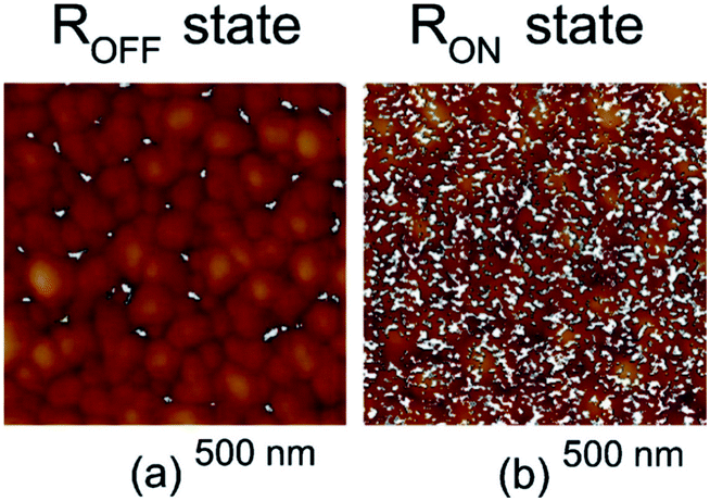 | ||
| Fig. 1 (a) The CAFM image of the NiO thin film for the Roff state corresponding to 100 switching cycles. The bias voltage of 0.1 V was used for the CAFM measurement. (b) The CAFM image of the NiO thin film for the Ron state corresponding to 100 switching cycles. Reproduced from ref. 22 with permission from [AIP], copyright [2008]. | ||
Although this methodology offers distinct advantages of real time frame images of devices at low and/or high RSs, it does, however, require a highly selective etching method for the removal of the top electrode. The chemical etchant may easily damage the sample's surface (insulating layer) or may disturb the composition of film. Furthermore, the electrical response in these measurements is the cumulative effect from the device and cannot be considered as a single filament effect.
Another strategy is to directly measure the RS properties of the films with CAFM without using conventional measurements (probe station-source meter). The ramped voltage is directly imposed on the bare sample surface (without any top electrode) with the tip of the CAFM. Then, the surface is scanned to read its topographical changes as a consequence of applied potential. The biggest advantage of this method is that the evolution of electrical response of a single filament depending on the applied bias can be determined. Because of the extremely small size of the CAFM tip, the observed current response can be attributed to the same conducting filament response which is under the CAFM tip. A good example of this is the pioneer work of Szot et al.23 In their study, the resistive switching characteristics of single crystalline strontium titanate (SrTiO3) were studied using CAFM. The switching behaviour was attributed to the single dislocation crossing the surface present in the SrTiO3. However, this method may have some output limitations in CAFM. For example, the maximum output voltage that a commercial CAFM (most of them) can supply is ±10 V, which may not be sufficient to initiate the electroforming process in some materials. Furthermore, it is generally believed that the reset process occur at a few tens of μA.24,25 But, most of the commercial CAFMs have limitations in current measurements for up to tens of nA, and beyond this limit, only a saturation horizontal line is observed even if a resistive change phenomenon in the device exists, and the electronic response of the cell during the reset process is masked.23,26 To overcome this issue, the use of an external source meter or semi-conductor parameter analysis for applying electrical stress and to measure the current was proposed and implemented.27,28 For example, the RS characteristics of a polycrystalline film of hafnium(IV) oxide (HfO2) were investigated using this method.28 The current signals before and after the dielectric breakdown regions were clearly observed. It was found that the origin of the conductive filaments to express the RS behaviour is the grain boundaries.
Current mapping is also used in CAFM measurements to induce the RS response in the materials. Yoshida et al.29 demonstrated that bipolar voltage application in a local region of NiO/Pt films using CAFM can write both LRS and HRS. Current mapping sequences with different sizes and voltages at the same point of a NiO stack were performed (Fig. 2).
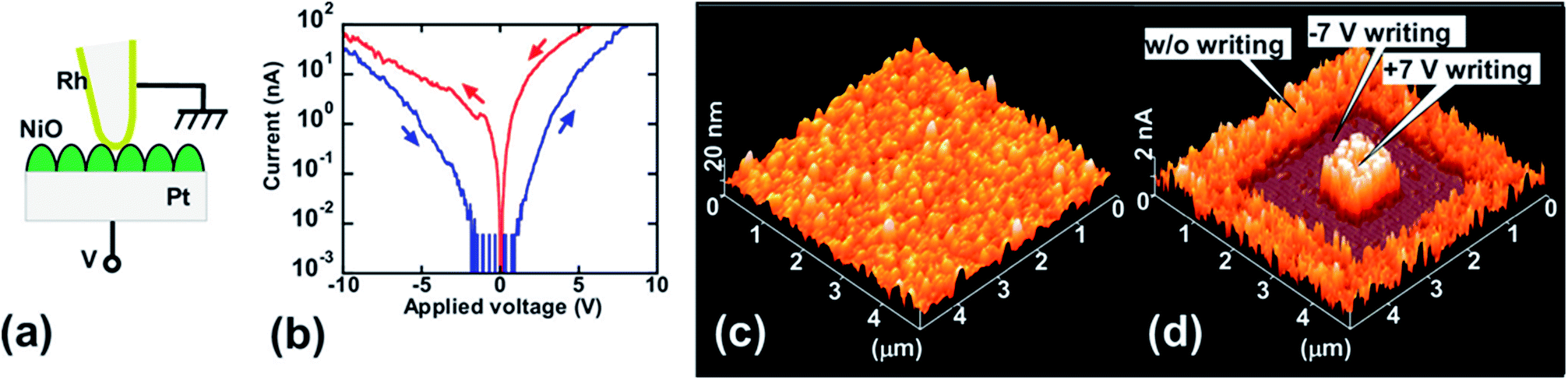 | ||
| Fig. 2 (a) Schematic diagram of CAFM measurement setup. (b) Typical I–V curves of Rh-tip/Ni1+δO/Pt structure. (c) Simultaneously observed topographic image and (d) current image of Ni1+δO/Pt film. Reproduced from ref. 29 with permission from [AIP], copyright [2008]. | ||
The topographic and current images of the Ni1+δO/Pt film with a sensing voltage of 1 V are shown in Fig. 2c and d. Under a DC bias of −7 V, the HRS was written in the centre, then a DC voltage of +7 V was applied using a rhodium (Rh) scanning tip in the centre to write the LRS. The topographic images were found to be unaffected during the AFM writing (Fig. 2d), however, the current mapping images can clearly distinguish HRS and LRS. It was also concluded that the entire written area is conductive and acted as assembled tenuous filaments rather than a single filament.24
This methodology is suitable for analysing those materials which require low forming potentials. However, by and large this technique cannot provide the dynamics of the set and reset process during switching events. Even the selection of off/on set voltages could be very challenging because of the inhomogeneities within the samples (thickness and concentration of carriers, and so on) and a poor selection of set/reset potentials can create more complexities in the device. The resistive switching characteristics in two-dimensional layered hexagonal boron nitride dielectric films using CAFM was investigated by Ranjan et al.30 In the LRS of the device, they observed standard random telegraph noise signatures, which were related to the SET distributions for high κ dielectrics such as: HfO2. The device was found to express good endurance characteristics but poor retention capabilities which were attributed to the concentration gradient driven, back diffusion of ions from their reservoir (electrodes).
Trapatseli et al.31 investigated the switching characteristics of 10 nm thick TiO2 thin films by simultaneously recording in situ spatial topography and current distributions (Fig. 3). The tip of the CAFM was used as the top electrode to induce switching in the films. The minimum voltage required to induce lateral current distribution changes but not topographic changes was called VSB and the potential required to induce changes both in lateral current distribution and topography was called VHB. Two different TiO2 thin films with varying oxygen stoichiometry (a near stoichiometric TiO2–x and a mixed valence TiOx) were investigated.
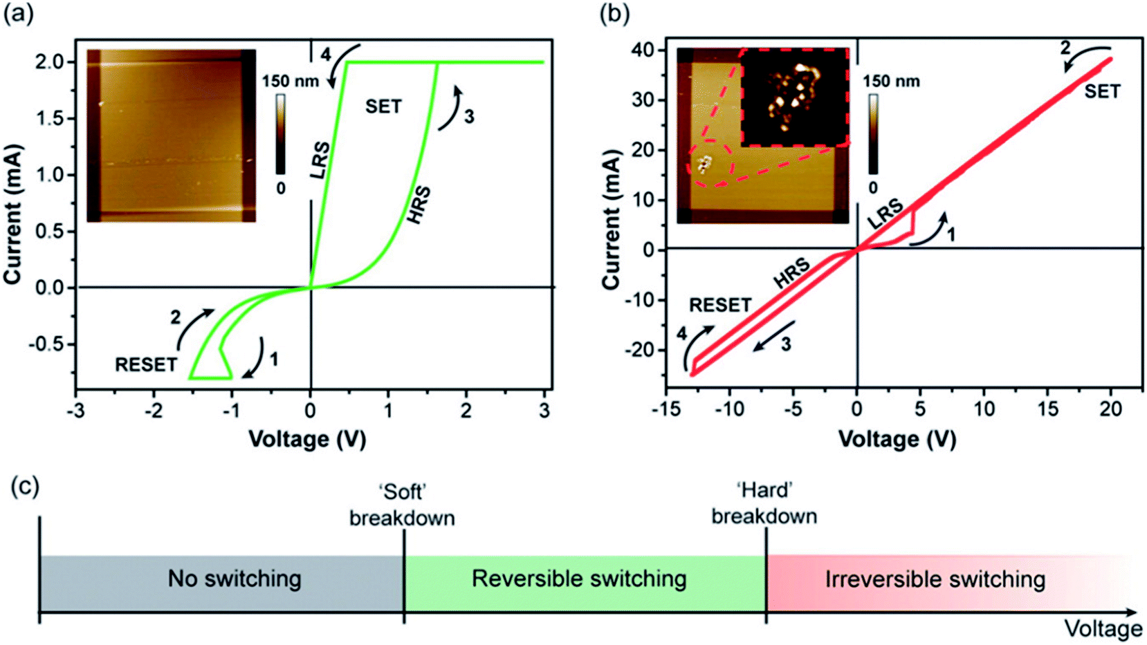 | ||
| Fig. 3 Representative I–V characteristic of a device (a) after SB and (b) after HB. Insets: AFM topographies of the devices' top electrodes. (c) Schematic of the resistive switching dynamics in RRAM cells. Reproduced from ref. 31 with permission from [ACS], copyright [2015]. HB: hard breakdown, SB: soft breakdown. | ||
A homogeneous resistive switching mechanism was observed in all the films. The VSB and VHB for the TiO2−x thin films were found to be 6.5 V and 7.0 V respectively. For mixed valence TiOx films, significantly lower values of VSB and VHB were recorded: 1.7 V and 2.2 V, respectively. This difference in switching dynamics for both films was attributed to the presence of oxygen vacancies. When a negative potential is applied to the CAFM tip (positive charge on the bottom electrode/sample), a low conductive region was formed (oxygen vacancies depleted region) that transformed the sample into high resistance state.31
Muenstermann et al. demonstrated RS in iron-doped SrTiO3 thin films deposited using pulsed laser deposition with the aid of CAFM.32 An electrode peel off strategy was used to visualize the dynamics of switching events under CAFM. The Pt top electrodes were used to induce RS effects in the devices and two devices (i) in HRS and (ii) LRS were chosen to further investigate the switchable regions under the AFM to compare their conductivity images as shown in Fig. 4. The sample having a junction in LRS shows both a conducting crater region and a conducting surrounding region (Fig. 4a). For the HRS junction, the conducting surrounding regions were not observed (Fig. 4b).
 | ||
| Fig. 4 (a) Conductive AFM current images of a junction that has been set to on state and (b) a junction that has been set to the off state before delamination. A vanishing of the broadened conducting area around the crater due to the off switching can be seen. Reproduced from ref. 32 with permission from [Wiley], copyright [2010]. | ||
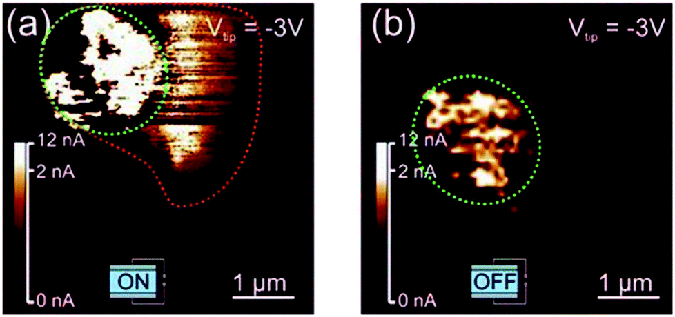
The effect of doping on RS characteristics can also be determined using CAFM. Although, many materials have demonstrated excellent RS characteristics of high on/off ratios, and excellent endurance performance with good retention, doping can also be adopted to enhance the devices' performance in terms of higher on/off ratios, energy transition, switching time and cycling endurance.14,33–35 The device performance can be modulated by the addition of dopants in a variety of ways. For example, a very high uniformity in device operational parameters was achieved in cerium(IV) oxide using cobalt doping.35 A greater on/off ratio with good endurance was achieved in zinc oxide (ZnO) using Ti doping.34 Furthermore, the dopant can induce oxygen vacancies in the parent matrix for expressing a modulated RS response.14,36 CAFM was utilized by Muenstermann et al.37 to investigate the morphology and different defect paths in niobium (Nb) doped SrTiO3 stacks.
By applying a readout voltage of −1 V, the specific conductive pattern of the sample was visualized as shown in Fig. 5a. When, the tip was subjected to a higher potential of −3 V, it switches off all its conductive maps and the previous state was retrieved by applying +3 V. This process was repeated again and the subsequent switching was demonstrated as reversible switching between on and off states as shown in Fig. 5b–d. This nanoscale behaviour was attributed to the presence of defect-rich regions that exhibit a higher concentration of oxygen vacancies to provide easily accessible diffusion channels.
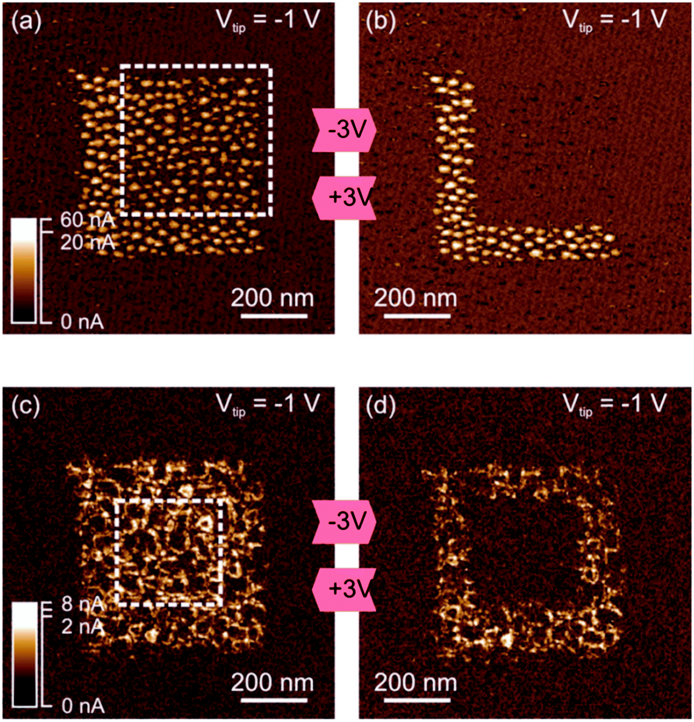 | ||
| Fig. 5 [(a) and (b)] Reversible RS in a 2 at% Nb-doped SrTiO3 sample grown in a coherent, 3D way. The CAFM current images show an array of conducting units which can be switched between two different resistance states. [(c) and (d)] Reversible RS in a 2 at% Nb-doped SrTiO3, sample grown in an island growth mode. The array of conducting rings corresponds to the film's defect structure and can be switched between two different resistance states. Reproduced from ref. 37 with permission from [AIP], copyright [2010]. | ||
3. TEM analysis of resistive switching materials
To understand the resistive switching mechanisms in a variety of materials, in situ TEM was used, and electric characteristics of the device were measured simultaneously with the TEM observation. Because of the high resolution of TEM, it is considered to be an excellent method to detect the formation and destruction of conductive filaments (or switching dynamics) at the nanoscale areas. The characterization system is usually composed of a custom-made TEM holder, a control system for the piezoactuator, a current measurement unit, and a charge coupled device (CCD) camera system.38–40 A TEM sample holder is used to insert the sample for characterization and a moveable platinum iridium (Pt–Ir) tip with nanometer scale precision is used in the piezoactuator to contact with the top electrode. Real time images are recorded using the CCD video camera during typical current–voltage measurements. An image showing an example of the setup is shown in Fig. 6.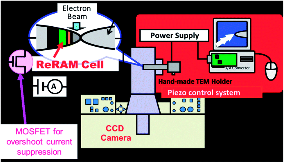 | ||
| Fig. 6 Schematic image of an in situ TEM system. JEM-2010 microscope (Jeol, 200 kV, 10−5 Pa) was used. A metal-oxide-semiconductor field-effect transistor (MOSFET) connected in series is used to suppress the overshoot current caused by the parasitic capacitance. Reproduced from ref. 38 with permission from [ECS], copyright [2015]. | ||
Takahashi et al. measured the I–V characteristics of a molybdenum oxide (MoOx) based memory cell in the TEM during their set and reset processes.38 A typical I–V hysteresis was observed in the cell, with a set process appearing at about +2.7 V. At this set voltage, a dark contrast was initially observed which originated from the film/electrode interface [MoOx/titanium nitride (TiN)] as shown in Fig. 7.
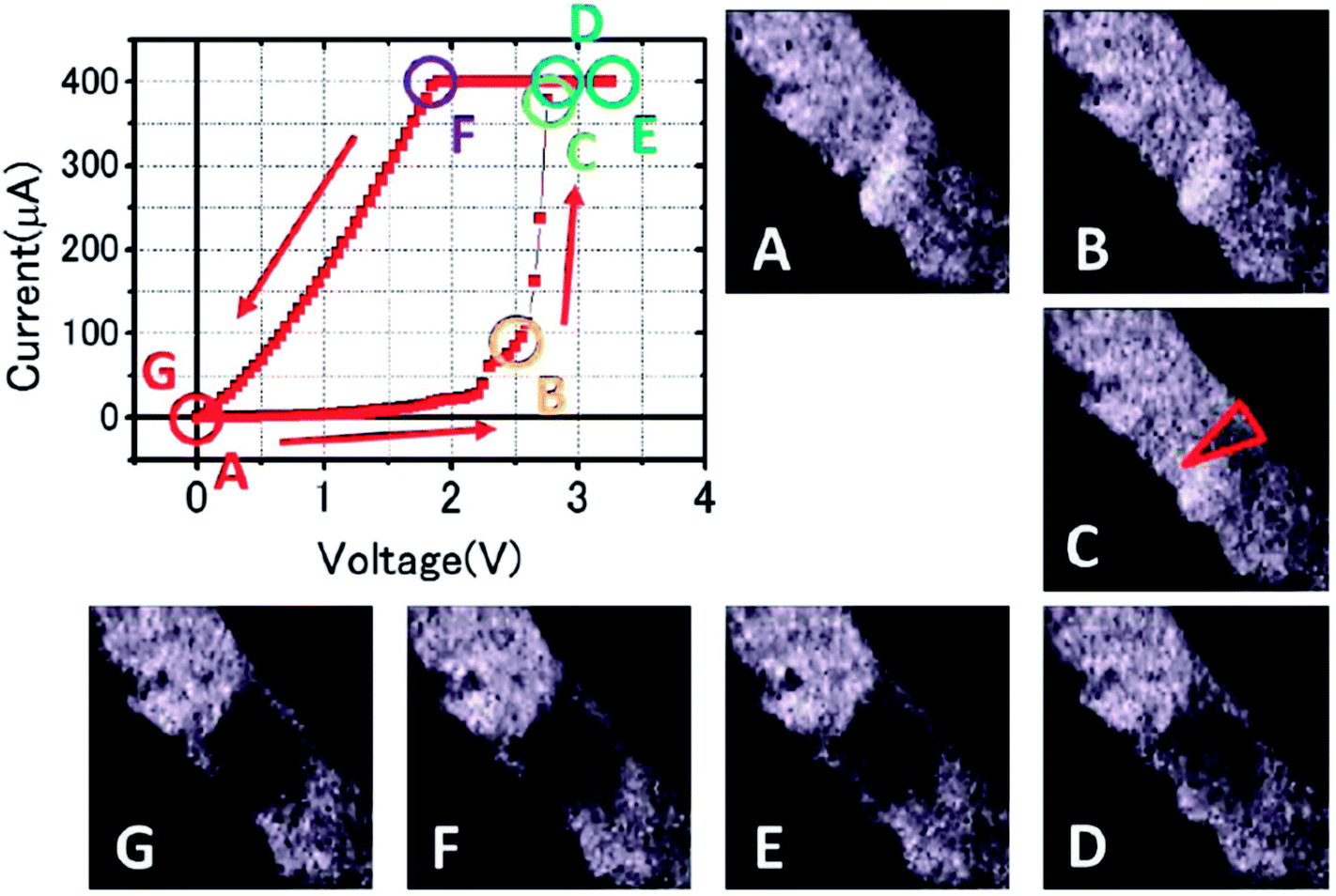 | ||
| Fig. 7 I–V hysteresis characteristics and in situ TEM images taken during a positive voltage sweep for the SET operation. Images A–G correspond to the position indicated by the circles shown in the I–V characteristics. Reproduced from ref. 38 with permission from [ECS], copyright [2015]. | ||
This dark contrast, which is generally referred to as a conductive filament was confirmed, using energy dispersive X-ray spectroscopy (EDX), to be formed of Cu. When the negative potential was applied to the top electrode, the already formed conductive filament was found to shrink and ultimately disappeared as shown in Fig. 8.
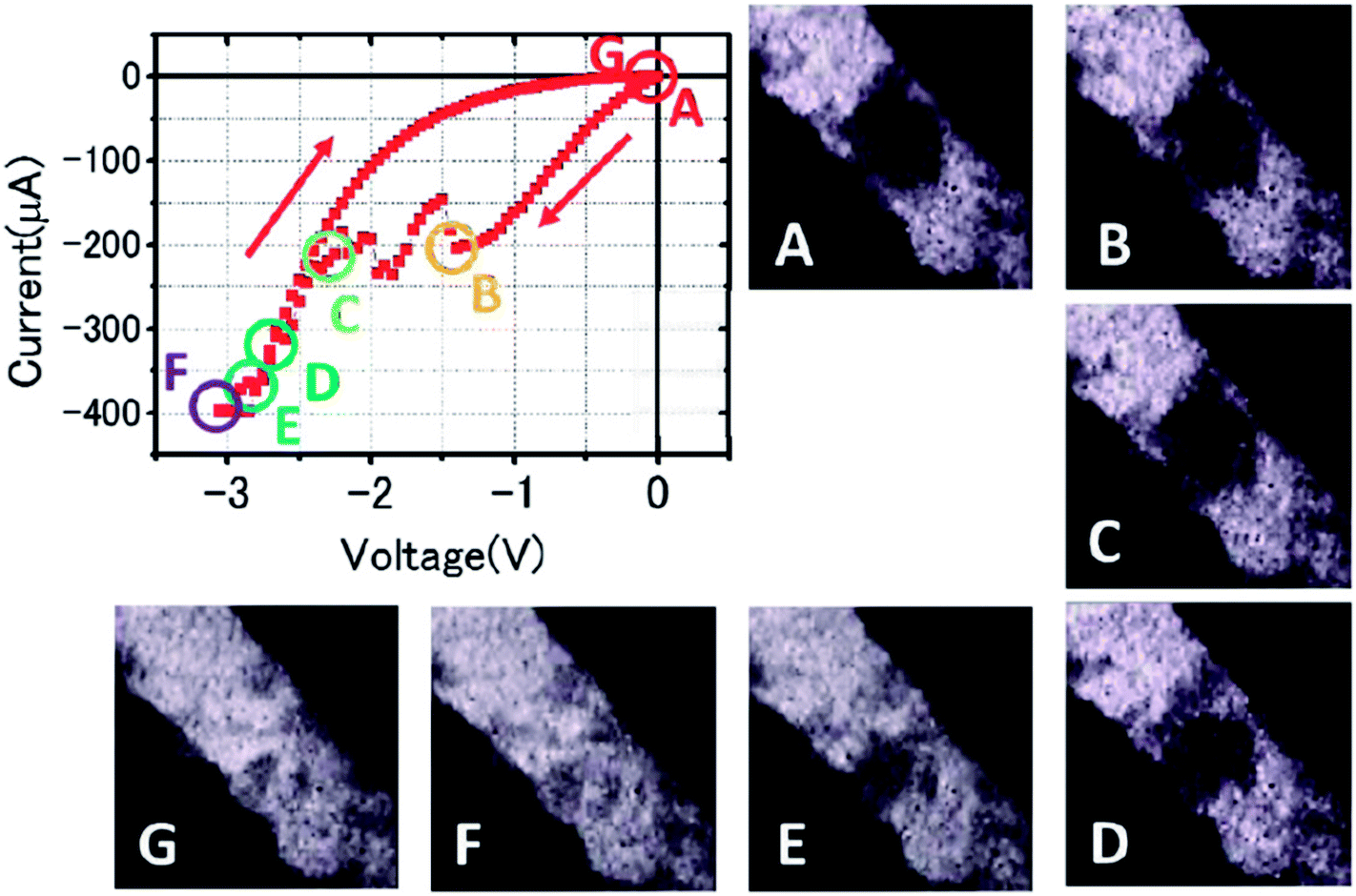 | ||
| Fig. 8 I–V hysteresis characteristics and in situ TEM images during a negative voltage sweep for the reset operation. Images A–G correspond to the position indicated by the circles shown in the I–V characteristics graph. Reproduced from ref. 38 with permission from [ECS], copyright [2015]. | ||
The direct observation of interfacial electrochemical redox reactions using in situ TEM of a TiN/praseodymium calcium manganese oxide (Pr0.7Ca0.3MnO3; PCMO)/Pt junction device was demonstrated by Baek et al.41 An intermediate reaction layer composed of TiOxNy was found to form and rupture in response to the applied potential. The thickness of this layer was of the order of a few nanometers as shown in Fig. 9.
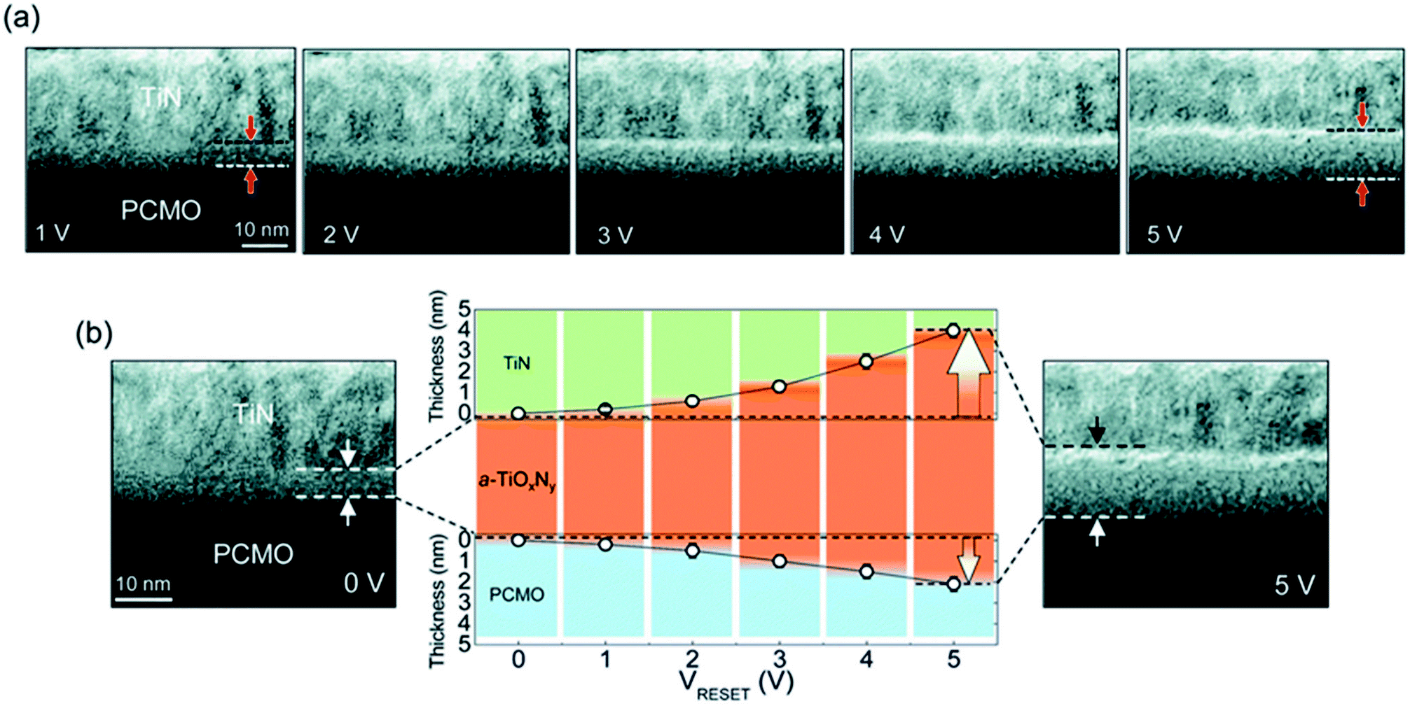 | ||
| Fig. 9 In situ TEM resistive switching of a TiN/PCMO/Pt junction device to the HRS. (a) A series of TEM snapshots captured at Vreset during sequential positive bias sweeps (0 → +Vreset → 0) by applying Vreset from 1 V to 5 V in 1 V increments. Changes in the thickness of the α-TiOxNy reaction layer are indicated by red arrows. (b) Movement of the two reaction fronts of the α-TiOxNy layer, i.e., the α-TiOxNy/TiN (upper) and the PCMO/α-TiOxNy (lower) interfaces, traced with the increase in Vreset. The α-TiOxNy/TiN interface moves faster than the PCMO/α-TiOxNy interface indicating that the drift of not only oxygen but also of Ti ions contribute to the growth process with the stronger influence of the oxygen ions. Reproduced from ref. 41 with permission from [RSC], copyright [2017]. | ||
Further correlation analyses were also carried out and it was concluded that an onset of electric field is mandatory (∼106 V cm−1) to grow the interlayer at the TiN/PCMO interface, which is responsible for the filamentary switching effects in these devices. Furthermore, it was found that the migration of oxygen as well as Ti ions is responsible for the growth of an interfacial layer in these devices.
Chen et al. observed the evolution of the conducting filaments during the switching process in ZnO-based resistive memories.42 A dark contrast was observed near the top electrode during the electroforming process, which was because of the nucleation and growth of the conducting filament. Afterwards a complete filament was formed which was thin in the middle. When the device was reset, the filament was ruptured from the middle (thinnest portion) and the joule heating was thought to be a possible reason for this rupture. These observations clearly support the theory that the thermochemical reactions are the main driver for the resistive switching effects in these samples.
Choi et al.43 used different bias voltages to characterize Cu/Cu–germanium telluride (GeTe)/Pt memory cells and the corresponding cross-sectional scanning transmission electron microscopy (STEM) results are shown in Fig. 10.
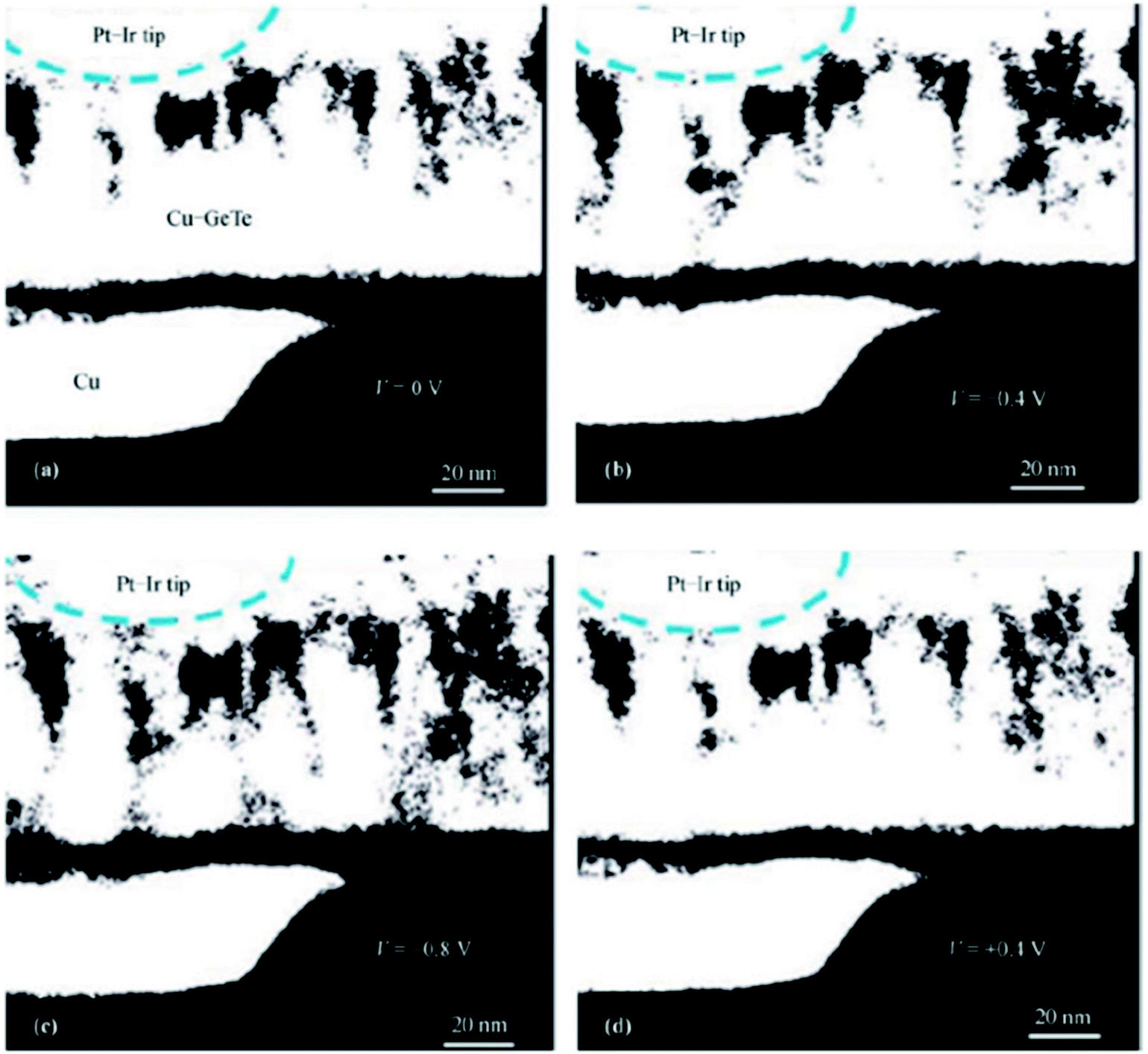 | ||
| Fig. 10 In situ STEM measurements of microstructure changes in a Pt/Cu–GeTe/Cu device after applications of (a) 0 V, (b) −0.4 V, (c) −0.8 V and (d) 0.4 V bias voltages on the Pt electrode. Reproduced from ref. 43 with permission from [Wiley], copyright [2011]. Pt–Ir: Platinum–iridium. | ||
From the results obtained, some dark regions were observed which correspond to the doped Cu and those clusters of Cu were hanging in between the top and bottom electrodes without applying any bias potential. With a positive potential, the Cu clusters began to expand until they formed filaments between the two electrodes, and thus, the memory was turned to the on state. For the reverse bias, the filaments ruptured, thus turning the device back to the off state. Even within the same device, the growth of multiple filaments was observed, which could possibly lead to multiple resistive states in the single device.
An excellent demonstration of the formation of filaments comprised of active electrode ions towards an inert electrode is found in the silicon dioxide (SiO2) based resistive memories.44 The active and inert electrodes were Ag and Pt, respectively, and a constant potential was applied to the Ag electrode and the current through the device was recorded with time. After 26 s of applied potential, they observed the first electroforming process in the SiO2-based device. A well-formed conducting filament was observed using TEM (highlighted by the top arrow in Fig. 11b). The detailed TEM analysis in conjunction with EDX revealed that the filament was indeed composed of elemental Ag. Several other incomplete filaments were also observed during the TEM investigations.
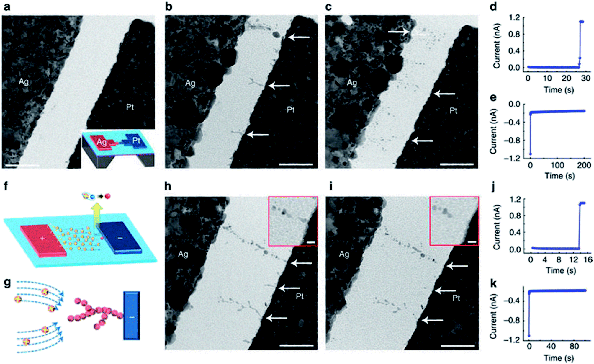 | ||
| Fig. 11 (a) TEM image of an as-fabricated SiO2-based planar device fabricated on a SiNx membrane. Scale bar, 200 nm. Inset: schematic of the device. (b) TEM image of the same device after the forming process. The arrows highlight several representative filaments. Scale bar, 200 nm. (c) TEM image of the same device after erasing. Scale bar, 200 nm. (d) Corresponding I–t curve during the forming process that led to the image in (b). The applied voltage was 8 V. (e) Corresponding I–t curve during the erasing process that led to the image in (c). The applied voltage was −10 V. (f) Schematic of the filament growth process showing the transport and reduction of Ag cations. (g) Schematic of the dendrite structure formation. (h) TEM image of another device with larger electrode spacing after the forming process. Scale bar, 200 nm. Inset: zoomed-in image of the filament (highlighted by the upper arrow) near the dielectric/inert electrode interface. Scale bar, 20 nm. (i) TEM image of the same device as in (h) after erasing. The dissolution of the filaments was found to take place at the inert electrode interface. Scale bar, 200 nm. Inset: the same region as the inset in (h) after erasing. Scale bar, 20 nm. (j) Corresponding I–t curve during the forming process that led to the image in (h). The applied voltage was 10 V. (k) Corresponding I–t curve during the erasing process that led to the image in (i). The applied voltage was −10 V. Reproduced from ref. 44 with permission from [NPG], copyright [2012]. | ||
Furthermore, the conducting filament(s) are found to exhibit a conical shape, which was thicker from the top (active electrode) and thinner/weaker from the bottom (inert electrode). The geometry of the filaments is of extreme importance in the operations of resistive memories, as the filament disappears or grows further from its thinner part.45 Therefore, the dielectric/inert electrode interface for some materials is more important than the dielectric/active electrode junction and the TEM analysis verified this theory. From Fig. 11c, it was confirmed that the filaments were ruptured near the dielectric/inert electrode junction, whether they are completely formed or partially constructed. Another important observation, which was recorded using TEM during the erasing process, is that the filaments did not fully dissolve (Fig. 11i). Although the filaments have been ruptured, they no longer connect the active electrode to the inert electrode (low conductivity), resulting in less efficient redox processes. This behaviour further supports the ECM process, in which it is generally believed that a higher potential is generally require for the forming process. Once an initial electroforming has been established, because of the presence of already broken or partial filaments, comparatively less voltage is required for the set and reset processes.5,46,47
4. Investigations of resistive switching using scanning electron microscopy
The use of the method of in situ SEM investigations of resistive switching characteristics is not very common. However, a few studies have demonstrated the use of this measurement setup for determining RS characteristics. Schmidt et al.48 studied the RS behaviour of individual, chemically synthesized TiO2 nanoparticles (NPs) using a nano-manipulator system in a field-emission SEM. The Pt–Ir metallic alloy on a silicon substrate was used as the bottom electrode. The TiO2 NPs of varying sizes (80 nm to 300 nm) as well as the deposited thin films of TiO2 were used as main dielectric materials. Finally, a Pt–Ir coated tip was used to measure the current–voltage characterizations of individual TiO2 NPs. The schematic of the measurement setup is shown in Fig. 12.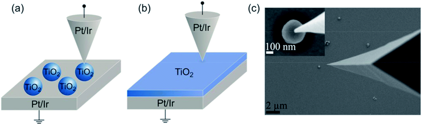 | ||
| Fig. 12 Schematic illustrations of the two resistive switching devices using: (a) immobilized TiOx NPs and (b) thin films. (c) An example of a low magnification SEM image of TiO2−x NPs on a Pt/Ir surface and the tip electrode. The high magnification inset shows an individual NP addressed by the tip of the electrode. Reproduced from ref. 48 with permission from [Wiley], copyright [2015]. | ||
According to the findings of Schmidt et al., the amorphous and thermally calcined TiO2 NPs expressed no switching responses, whereas the TiO2 NPs, which were vacuum annealed exhibit interesting resistive switching responses. These samples demonstrated complementary switching and bipolar resistive switching characteristics. However, the vacuum annealed thin films of TiO2 only expressed bipolar switching. This interesting switching behaviour was attributed to the core–shell-like structure of the TiO2 NPs formed because of the reoxidation of the reduced NPs in air.48 In this report, although direct observation of conducting filaments/channels was not reported, this method could provide a great opportunity to systematically determine the resistive switching properties down to the single nanoparticle scale without the use of any complex lithographic fabrication techniques.
The evolution of conducting filaments at different programming currents in SiO2 based memories was demonstrated by Yang et al.44 By regulating the programming currents, the filament growth could be controlled. In this report, the authors took four samples of similar structure and the currents were recorded at different fixed applied potentials. By having higher fixed potentials, the filaments' evolution in size and length was measured and is shown in Fig. 13. These results clearly indicated that the electron current can facilitate the filaments' formation process and the active electrode reduces and fuses into the dielectric layer by capturing free electrons.44
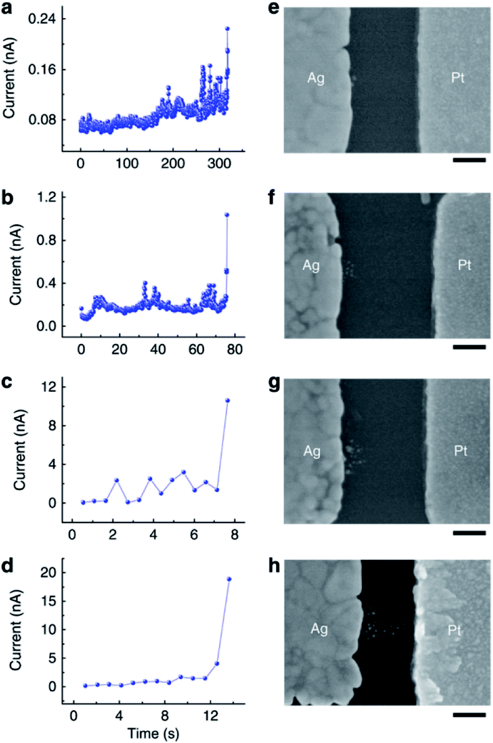 | ||
| Fig. 13 (a–d) I–t curves with different programming currents during the forming process and (e–h) corresponding SEM images of the devices after forming, showing the correlation of the filament size with the programming current. Scale bar, 100 nm. Four different α-Si-based devices with similar geometry were used in this study. The applied voltages were (a) 18 V, (b) 26 V, (c) 22 V, and (d) 20 V. Reproduced from ref. 44 with permission from [NPG], copyright [2012]. | ||
In another report by Guo and Schindler, memory based on de-ionized water (H2O) with a planar structure was fabricated.45 In this report, the formation of conical shaped Ag filaments in an Ag/H2O/Pt device was observed using SEM and the results are shown in Fig. 14. During the switching process, first metallic Ag was oxidized to Ag+ ions, then the Ag+ ions migrated towards the counter electrode and finally they were reduced at the Pt electrode. The evolution of Ag filaments was in the form of dendrites and when any of the formed dendrites touch the inert electrode, the cell was switched on as shown in Fig. 14. The reverse potential starts the dissolution of the Ag atoms leading to the reset process in the device.
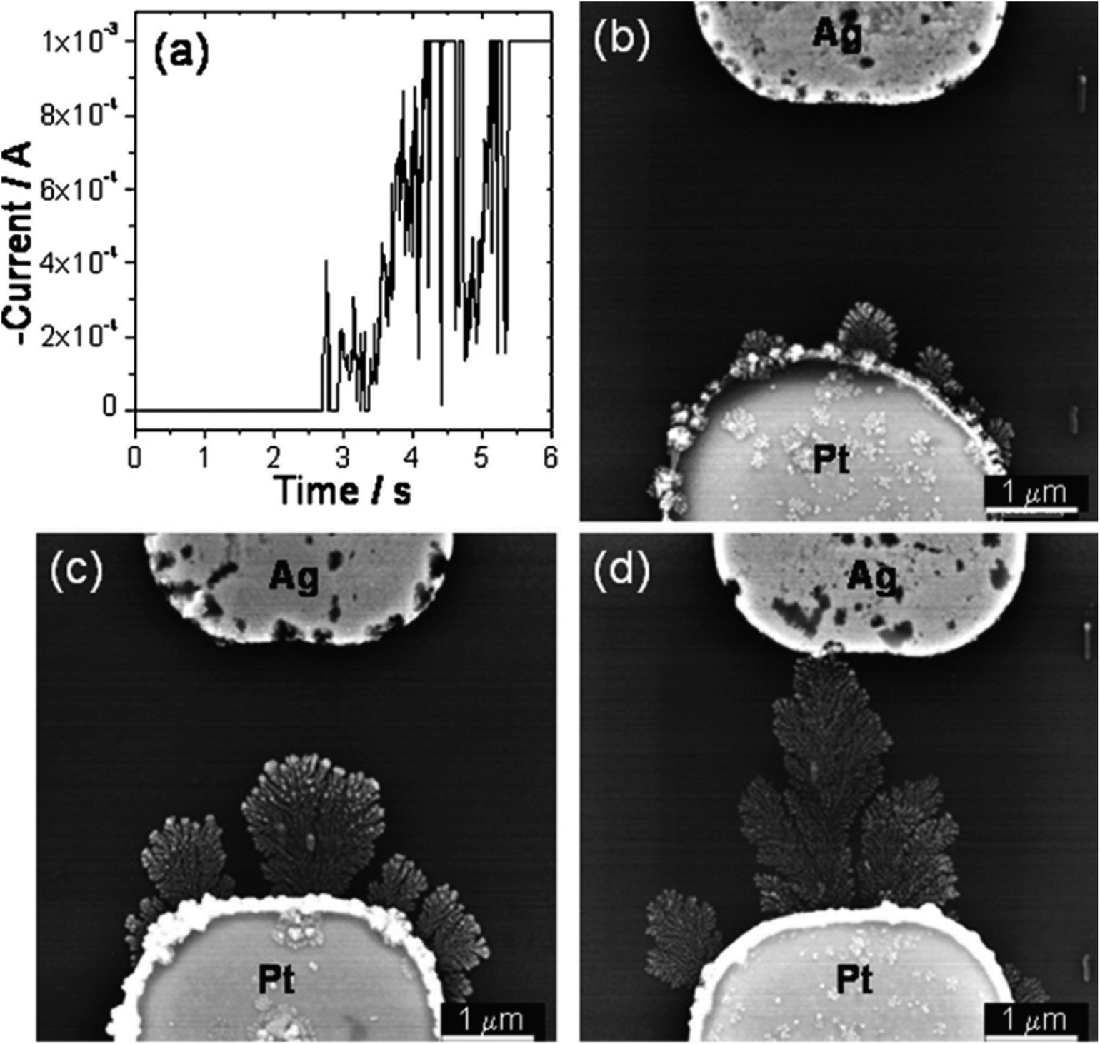 | ||
| Fig. 14 The switching-on process while applying −1 V to a Pt/H2O/Ag cell with a Pt/Ag gap of 3 μm: (a) I–t curve, [(b), (c), and (d)] SEM images showing the Ag dendrite growth after applying −1 V for about 1, 2, and 4 s, respectively. Reproduced from ref. 45 with permission from [AIP], copyright [2007]. | ||
5. Summary and outlook
This mini review mainly describes some basics of resistive switching mechanisms in various dielectric materials. Available methodologies such as I–V characteristics with the aid of probe station are highlighted and presented. In order to understand the resistive switching mechanisms, high resolution microscopes such as: transmission electron microscopy, scanning electron microscopy and conductive atomic force microscopy were found to be very powerful methods. In this review two main strategies to study the origin of resistive switching at the nanoscale are reviewed. The first approach is to induce a resistive switching response in the devices by the means of external potential stimuli and then the samples were subjected to high resolution microscopes such as: conductive atomic force microscopy to obtain the overall picture of device structural changes in either lateral or vertical directions. In the second methodology, the switching dynamics are studied in the real time. For example, the formation or disappearance of filament device behaviour can be monitored by simultaneously applying a potential of different polarities. Each of the methodologies has distinct advantages and some flaws too. For example, it is really challenging to observe the filaments evolution at the sub 10 nm scale in in situ scanning electron microscopy because of its resolution limits. However, by using conductive atomic force microscopy, the origin of resistive switching in a HfO2 matrix was identified to be at the grain boundaries because of an unusually high concentration of positive charges. In situ transmission electron microscopy is a more comprehensive and reliable technique to provide a good understanding of the local conducting paths with visible pictures. Furthermore, the energy dispersive X-ray spectroscopy and electron energy-loss spectroscopy measurements in conjunction with transmission electron microscopy can provide further useful insights into the filaments' composition and their dynamics during switching events.The development of predictable, reliable and functional memristive devices for integrated electronics requires optimization in device performance for data endurance, data retention, high on/off ratios and low switching power. Furthermore, these functional memories cannot be imagined without a good understanding of the device operational mechanisms. The further development of these resistive memories will have certain issues particularly when they will be integrated into a crossbar matrix. These issues could be in the form of leakage currents or cross-talk problems in the material. In spite of strategies such as: the addition of a diode to tackle the sneak path issues, these memories are still very young and could face many challenges as time goes on. Furthermore, resistive memories could also find their applications in other fields such as: integrated supercapacitors, lithium ion batteries and so on.
Conflicts of interest
The authors declare no conflict of interest.Acknowledgements
The authors would like to acknowledge the financial support from the Australian Research Council Projects of DP150103006 and DP170104831.References
- K. Terabe, et al., Quantized conductance atomic switch, Nature, 2005, 433, 47 CrossRef PubMed.
- X. Chen, et al., Direct resistance profile for an electrical pulse induced resistance change device, Appl. Phys. Lett., 2005, 87(23), 233506 CrossRef.
- E. Y. Tsymbal and H. Kohlstedt, Tunneling Across a Ferroelectric, Science, 2006, 313(5784), 181–183 CrossRef PubMed.
- D. B. Strukov, et al., The missing memristor found, Nature, 2008, 453, 80 CrossRef PubMed.
- R. Waser, et al., Redox-Based Resistive Switching Memories – Nanoionic Mechanisms, Prospects, and Challenges, Adv. Mater., 2009, 21(25–26), 2632–2663 CrossRef.
- E. Lörtscher, et al., Reversible and Controllable Switching of a Single-Molecule Junction, Small, 2006, 2(8–9), 973–977 CrossRef PubMed.
- L. Esaki, R. B. Laibowitz and P. J. Stiles, IBM Tech. Discl. Bull., 1971, 13, 2161 Search PubMed.
- M. Wuttig and N. Yamada, Phase-change materials for rewriteable data storage, Nat. Mater., 2007, 6, 824 CrossRef PubMed.
- J. Doo Seok, et al., Emerging memories: resistive switching mechanisms and current status, Rep. Prog. Phys., 2012, 75(7), 076502 CrossRef PubMed.
- S. Lee, et al., Resistance Switching Behaviors of Hafnium Oxide Films Grown by MOCVD for Nonvolatile Memory Applications, J. Electrochem. Soc., 2008, 155(2), H92–H96 CrossRef.
- Z. Xu, et al., Engineering cationic defects in transparent tin oxide superlattices, Mater. Des., 2018, 155, 71–76 CrossRef.
- Z. Xu, et al., Manipulating resistive states in oxide based resistive memories through defective layers design, RSC Adv., 2017, 7(89), 56390–56394 RSC.
- A. Younis, D. Chu, A. Hadi Shah, H. Du and S. Li, Interfacial redox reactions associated ionic transport in oxide-based memories, ACS Appl. Mater. Interfaces, 2016, 9(2), 1585–1592 CrossRef PubMed.
- A. Younis, D. Chu and S. Li, Tuneable resistive switching characteristics of In2O3 nanorods array via Co doping, RSC Adv., 2013, 3(32), 13422–13428 RSC.
- H. Zhang, et al., Gd-doping effect on performance of HfO2 based resistive switching memory devices using implantation approach, Appl. Phys. Lett., 2011, 98(4), 042105 CrossRef.
- B. Gao, et al., A physical model for bipolar oxide-based resistive switching memory based on ion-transport-recombination effect, Appl. Phys. Lett., 2011, 98(23), 232108 CrossRef.
- Z. Lepeng, et al., Impact of deposition parameters on the performance of ceria based resistive switching memories, J. Phys. D: Appl. Phys., 2016, 49(29), 295106 CrossRef.
- M. P. Murrell, et al., Spatially resolved electrical measurements of SiO2 gate oxides using atomic force microscopy, Appl. Phys. Lett., 1993, 62(7), 786–788 CrossRef.
- S. J. O'Shea, et al., Conducting atomic force microscopy study of silicon dioxide breakdown, J. Vac. Sci. Technol. B Nanotechnol. Microelectron., 1995, 13(5), 1945–1952 CrossRef.
- T. G. Ruskell, et al., High resolution Fowler-Nordheim field emission maps of thin silicon oxide layers, Appl. Phys. Lett., 1996, 68(1), 93–95 CrossRef.
- B. J. Choi, et al., Resistive switching mechanism of TiO2 thin films grown by atomic-layer deposition, J. Appl. Phys., 2005, 98(3), 033715 CrossRef.
- J. Y. Son and Y.-H. Shin, Direct observation of conducting filaments on resistive switching of NiO thin films, Appl. Phys. Lett., 2008, 92(22), 222106 CrossRef.
- K. Szot, et al., Switching the electrical resistance of individual dislocations in single-crystalline SrTiO3, Nat. Mater., 2006, 5, 312 CrossRef PubMed.
- S. Long, et al., Voltage and Power-Controlled Regimes in the Progressive Unipolar RESET Transition of HfO2-Based RRAM, Sci. Rep., 2013, 3, 2929 CrossRef PubMed.
- A. Sawa, Resistive switching in transition metal oxides, Mater. Today, 2008, 11(6), 28–36 CrossRef.
- M. Lanza, A Review on Resistive Switching in High-k Dielectrics: A Nanoscale Point of View Using Conductive Atomic Force Microscope, Materials, 2014, 7(3), 2155 CrossRef PubMed.
- M. Lanza, et al., Resistive switching in hafnium dioxide layers: Local phenomenon at grain boundaries, Appl. Phys. Lett., 2012, 101(19), 193502 CrossRef.
- M. Lanza, et al., Grain boundaries as preferential sites for resistive switching in the HfO2 resistive random access memory structures, Appl. Phys. Lett., 2012, 100(12), 123508 CrossRef.
- C. Yoshida, et al., Direct observation of oxygen movement during resistance switching in NiO/Pt film, Appl. Phys. Lett., 2008, 93(4), 042106 CrossRef.
- A. Ranjan, et al., Conductive Atomic Force Microscope Study of Bipolar and Threshold Resistive Switching in 2D Hexagonal Boron Nitride Films, Sci. Rep., 2018, 8(1), 2854 CrossRef PubMed.
- M. Trapatseli, et al., Conductive Atomic Force Microscopy Investigation of Switching Thresholds in Titanium Dioxide Thin Films, J. Phys. Chem. C, 2015, 119(21), 11958–11964 CrossRef.
- R. Muenstermann, et al., Coexistence of Filamentary and Homogeneous Resistive Switching in Fe-Doped SrTiO3 Thin-Film Memristive Devices, Adv. Mater., 2010, 22(43), 4819–4822 CrossRef PubMed.
- A. Younis, D. Chu and S. Li, Evidence of Filamentary Switching in Oxide-based Memory Devices via Weak Programming and Retention Failure Analysis, Sci. Rep., 2015, 5, 13599 CrossRef PubMed.
- A. Younis, D. Chu and S. Li, Bi-stable resistive switching characteristics in Ti-doped ZnO thin films, Nanoscale Res. Lett., 2013, 8(1), 154 CrossRef PubMed.
- A. Younis, D. Chu and S. Li, Stochastic memristive nature in Co-doped CeO2 nanorod arrays, Appl. Phys. Lett., 2013, 103(25), 253504 CrossRef.
- M. Janousch, et al., Role of Oxygen Vacancies in Cr-Doped SrTiO3 for Resistance-Change Memory, Adv. Mater., 2007, 19(17), 2232–2235 CrossRef.
- R. Muenstermann, et al., Correlation between growth kinetics and nanoscale resistive switching properties of SrTiO3 thin films, J. Appl. Phys., 2010, 108(12), 124504 CrossRef.
- Y. Takahashi, M. Kudo and M. Arita, (Invited) Visualization of Conductive Filament of ReRAM during Resistive Switching by in situ TEM, ECS Trans., 2015, 69(10), 299–309 CrossRef.
- T. Fujii, M. Arita, Y. Takahashi and I. Fujiwara, “Analysis of resistance switching and conductive filaments inside Cu-Ge-S using in situ transmission electron microscopy, J. Mater. Res., 2012, 27, 886 CrossRef.
- J. Norpoth, et al., In situ TEM analysis of resistive switching in manganite based thin-film heterostructures, Nanoscale, 2014, 6(16), 9852–9862 RSC.
- K. Baek, et al., In situ TEM observation on the interface-type resistive switching by electrochemical redox reactions at a TiN/PCMO interface, Nanoscale, 2017, 9(2), 582–593 RSC.
- J.-Y. Chen, et al., Dynamic Evolution of Conducting Nanofilament in Resistive Switching Memories, Nano Lett., 2013, 13(8), 3671–3677 CrossRef PubMed.
- S. J. Choi, et al., In Situ Observation of Voltage-Induced Multilevel Resistive Switching in Solid Electrolyte Memory, Adv. Mater., 2011, 23(29), 3272–3277 CrossRef PubMed.
- Y. Yang, et al., Observation of conducting filament growth in nanoscale resistive memories, Nat. Commun., 2012, 3, 732 CrossRef PubMed.
- X. Guo, et al., Understanding the switching-off mechanism in Ag+ migration based resistively switching model systems, Appl. Phys. Lett., 2007, 91(13), 133513 CrossRef.
- V. Ilia, et al., Electrochemical metallization memories—fundamentals, applications, prospects, Nanotechnology, 2011, 22(25), 254003 CrossRef PubMed.
- C. Schindler, G. Staikov and R. Waser, Electrode kinetics of Cu–SiO2-based resistive switching cells: overcoming the voltage-time dilemma of electrochemical metallization memories, Appl. Phys. Lett., 2009, 94(7), 072109 CrossRef.
- D. O. Schmidt, et al., Resistive Switching of Individual, Chemically Synthesized TiO2 Nanoparticles, Small, 2015, 11(48), 6444–6456 CrossRef PubMed.
| This journal is © The Royal Society of Chemistry 2018 |