
 Open Access Article
 This Open Access Article is licensed under a Creative Commons Attribution-Non Commercial 3.0 Unported Licence
Polymer nanocomposite-enabled high-performance triboelectric nanogenerator with self-healing capability†
Huidan Niu‡
ab,
Xinyu Du‡ab,
Shuyu Zhao‡c,
Zuqing Yuanab,
Xiuling Zhangab,
Ran Caoab,
Yingying Yinab,
Chi Zhangab,
Tao Zhouab and
Congju Li *abc
*abc
aBeijing Institute of Nanoenergy and Nanosystems, Chinese Academy of Sciences, Beijing 100083, P. R. China. E-mail: congjuli@126.com
bSchool of Nanoscience and Technology, University of Chinese Academy of Sciences, Beijing 100049, P. R. China
cSchool of Energy and Environmental Engineering, University of Science and Technology Beijing, Beijing 100083, China
First published on 17th August 2018
Abstract
Triboelectric nanogenerators (TENG) have been proven to be effective for the collection of low-frequency vibrational energy in the environment. However, most polymer materials as friction layers are highly susceptible to mechanical damage during operation, which reduces the performance and lifetime of TENG. Herein, we report a high-performance, flexible triboelectric nanogenerator with reproducible self-healing electronic characteristics. Based on its soft and flexible polymers, the self-healing triboelectric nanogenerator (SH-TENG) can achieve a peak power of 2.5 W m−2 and triboelectric charge density of about 100 μC m−2. High-conductance Ag nanowires (AgNWs) are semi-embedded in the polymer to fabricate all-in-one friction layers and for an enhanced self-healing process. Both the output voltage and current of the healed device can reach up to about 99% of their original values even after five cutting/healing cycles. The fabricated SH-TENG has excellent stability and flexibility, which presents a significant step towards the fabrication of reliable triboelectric nanogenerators with recoverability and low maintenance costs.
Introduction
With the increasing energy demand worldwide, finding new techniques for energy harvesting is the key to meeting human requirements for the development of modern society.1,2 The abundant mechanical energy in the environment such as wind energy, hydroelectric energy and ocean energy has aroused people's attention due to its wide distribution and low cost.3,4 In recent years, various mechanical energy harvesting technologies have been developed, which convert energy in the environment into usable energy.5,6 Currently, based on triboelectrification and electrostatic induction, the TENG reported by Wang et al.7 have proven to be effective for collecting low-frequency vibrational energy,8 which is considered as a potential sustainable power source for future developments.9,10 The significant progress in TENG has opened a new chapter of energy harvesting technology in the ultimate challenge of miniaturization, and significant advances in the basic principles and applications of TENG have been achieved.11,12 Due to many desirable features of TENG, such as simple manufacturing process,13,14 flexible material choice,15 high output voltage16 and ability to operate under very low frequency and irregular mechanical motions,17,18 it has been used as a power source for many self-powered devices, which have the advantages of high efficiency, convenience, environmental friendliness and low cost.19,20Recent research on TENG has mainly focused on conventional electrodes and friction materials. However, in the collection process of mechanical energy, TENG has long been subjected to mechanical impact. These materials are susceptible to fracture and damage, which lead to a sharp decrease in their sustainability, safety, and lifetime.20,21 These effects inevitably lead to material failure, reducing the performance and decreasing the service life of the TENG. Thus, the application scope of TENG is greatly limited. Several solutions to this problem have been proposed to reduce the damage during the operation to improve the cycle life of the TENGs, which indeed decreased mechanical failure through a non-contact or slight-contact mode.22,23 However, soft-contact is an effective way to enhance the potential performance of the TENGs. Furthermore, with rapid development of materials science, flexible electronics and nanotechnology, self-powered intelligent sensor devices have mushroomed, which require the development of self-healing polymeric materials for TENGs to improve their safety, lifetime, energy efficiency, and environmental impact.24 Thus, the exploration of self-healing electrodes and polymeric friction materials is in high demand for the design of new types of TENG based on completely flexible and healable materials, which can recover after mechanical damage.21,25
Herein, a high-performance flexible triboelectric nanogenerator with reproducible self-healing electronic characteristics is fabricated with high stability and recoverability. The top and bottom electrodes are prepared by semi-embedding the silver nanowires into a polydimethylsiloxane (PDMS) film and thermoplastic polyurethane (TPU) film respectively, which are used to fabricate a contact-separation mode TENG.26 In the contact-separation mode, the triboelectric nanogenerator can achieve a peak power of 2.5 W m−2 and the triboelectric charge density of about 100 μC m−2 due to its soft and flexible polymers.27 When this self-healing triboelectric nanogenerator (SH-TENG) is cut off or scratched, PDMS and TPU with AgNWs show the ability of self-healing simply by linking the broken ends under near infrared (NIR) irradiation and recover the electrical properties. The healing process of the TPU is attributed to hot melting and that of PDMS is the result of hydrogen bonds.28 In addition, the electrode is prepared by embedding AgNWs in the polymer, which prevents the AgNWs from falling off due to touching or bending and maintain good conductivity and stability after several healing cycles. Compared with the performance of the original sample, the open circuit voltage, short circuit current and transferred charge of the healing sample are very close. Furthermore, the film exhibits stable electrical properties after multiple cycles of mending the cracks in the same region via simple thermal treatment. The fabricated SH-TENG is believed to have potential applications to power electronic devices, which require enhanced durability and reliability. The results indicate that our fabricated films can act as a promising self-healing material and have great applications in electronics and industries.
Results and discussion
Preparation of self-healing PDMS and TPU films
An AgNW-embedded TPU (AgNWs/TPU) film and an AgNW-embedded PDMS (AgNWs/PDMS) film were fabricated, as schematically illustrated in Fig. 1. We chose two different suitable substrates to form the uniform AgNWs semi-inlaid polymer films.29 The AgNW solution was casted onto the substrate to obtain the AgNW electrode layer, as shown in Fig. 1a. Subsequently, the TPU solution and liquid PDMS were coated on the AgNW film, as shown in Fig. 1b and c, respectively. Then, the TPU and PDMS films were cured in an air oven, as shown in Fig. 1d and e. The details of the fabrication method are described in the Experimental section. Attributed to the permeation of the liquid precursor into the AgNW network,30 the AgNWs were semi-embedded tightly in the cured TPU and PDMS films.31,32 The AgNWs/TPU and AgNWs/PDMS films were obtained by peeling them off the substrates, as shown in Fig. 1f and g, respectively, which reflects their good flexibility. Also, the AgNW-embedded surface was conductive and the opposite surface was nonconductive due to the thickness of the polymer layer. The resistances of the conductive surface were 1.4 Ω sq−1 and 13.9 Ω sq−1 for the TPU film and the PDMS film, respectively. Furthermore, the conductivity of the films would not decrease due to touching and bending motions.33 As shown in Fig. 1h and i, the AgNW-embedded TPU and PDMS films were characterized by scanning electron microscopy (SEM), respectively, which shows that the embedded structure was formed uniformly over the entire region and the AgNWs embedded into the TPU and PDMS formed a network structure.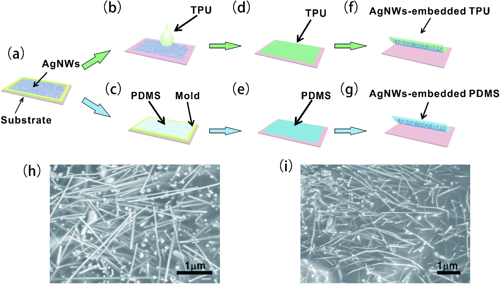 | ||
| Fig. 1 Schematic illustration of the fabrication process of the AgNW-embedded TPU film and PDMS film. (a) Casting AgNW solution on a substrate. (b, d and f) Illustrations of the fabrication of the AgNW-embedded TPU layer by casting TPU solution on the AgNW film. (c, e and g) AgNW-embedded PDMS layer prepared by the bar-coating process. (h) SEM image of the AgNW-embedded surface of the TPU film. (i) SEM image of the AgNW-embedded surface of the PDMS film. | ||
The cutting/healing process of the self-healing PDMS and TPU films
A schematic illustration of the self-healing process is shown in Fig. 2. The primary samples were placed onto a glass substrate, and the AgNW-embedded surface directly absorbed NIR light as the top side.34 Subsequently, the AgNWs/TPU and AgNWs/PDMS films were cut across their entire width with a scalpel (Fig. 2a). Right after contacting the ends of the fracture as close as possible, the samples were positioned under a conventional NIR lamp, of which the power density delivered to the samples was ∼0.63 W cm−2, which allowed self-healing to occur (Fig. 2b). To improve the healing efficiency of PDMS, we added 3 wt% graphite powder (GP) during the moulding process of the PDMS film, which gave the optimal experimental result for healing through the absorption of NIR light (Fig. S2†).34,35 GP-PDMS composites were fabricated through simple mechanical mixing. The GP-PDMS film was also cut into strips using a scalpel and positioned under a conventional NIR lamp.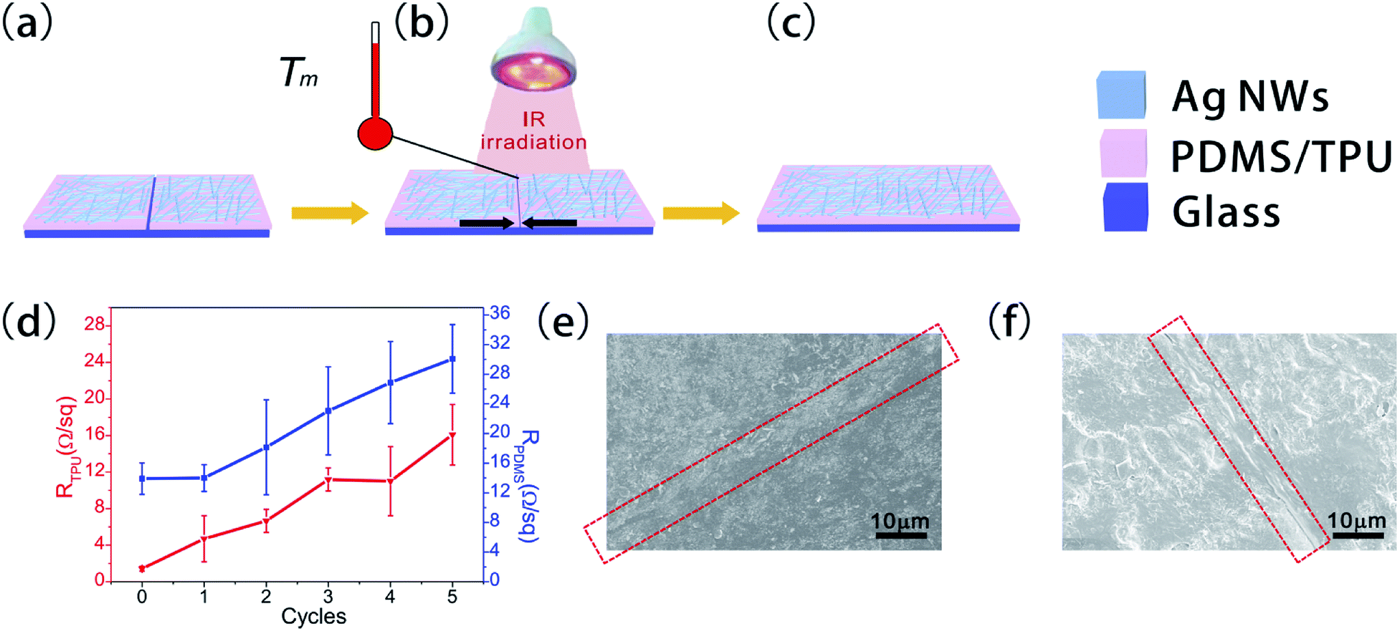 | ||
| Fig. 2 Schematic illustration of the cutting/healing process. (a) Cutting the AgNWs/TPU or AgNWs/PDMS films. (b) Self-healing process induced by contacting the ends of the fracture and exposure to NIR light irradiation. (c) Schematic illustration of the healed AgNWs/TPU or AgNWs/PDMS film. (d) Resistance changes across the fracture area after five cycles of the cutting/healing process for TPU film and PDMS film. (e and f) SEM images of the AgNW layer of the AgNW/TPU film and the AgNW/PDMS film after healing, respectively. | ||
Characterization of self-healing PDMS and TPU films
The self-healing result is due to the characteristics of effective absorption and conduction of NIR light into thermal energy by GP and AgNWs.36 It should be noted that the AgNWs acted as an electrical conductor to initiate the healing of the PDMS and TPU films, which consequently contributed to the electrical properties of the AgNW layer.37 The TPU melted at the broken interface and bonded again to heal the fracture above the melting point Tm of the polymer under the NIR lamp. For PDMS, the self-healing process was the result of the interaction among the abundant hydrogen bonds from the Si–OH at the end of the chains, which were demonstrated by FTIR in Fig. S5.† The high density of hydrogen bonding sites gave the elastomer a partial self-healing capability at the broken interface.28,38 Due to the energy from the NIR lamp, the PDMS reconnected through the hydrogen bonds at the fracture of the samples.39,40 For the performance of the SH-TENG, the electric healing conductivity of its electrode is also an important reference index, in addition to ensuring the friction layer contact area. As shown in Fig. 2d, after five cycles of the cutting/healing process, the resistance (R) across the fracture area only increased from 1.4 to 11 Ω sq−1 and 13.9 to 30 Ω sq−1 for the TPU and PDMS films, respectively. The SEM images in Fig. 2e and f show that the separated AgNW layer was closely connected after the cutting/healing of the TPU and PDMS films (Fig. S6 and S7†).To test the self-healing properties of the conductive films, the NIR light-induced healing of the AgNWs/TPU and AgNWs/PDMS films was examined by integrating the films into a circuit with a light-emitting diode (LED) and a constant DC power supply of 2.0 V,34,41 as shown in Fig. 3a and d , respectively. When the AgNWs/TPU and AgNWs/PDMS films were cut across their entire width with a scalpel, the LED immediately turned off (Fig. 3b and e, respectively). The cut resulted in a break in the electrical circuit, which broke the connection between the AgNWs and the bottom TPU and PDMS layer. This indicates that the AgNWs/TPU film and the AgNWs/PDMS film incurred severe damage. Interestingly, the LED became bright again after the cut was exposed to NIR light (Fig. 3c and f), which induced the healing process in the film under NIR light irradiation. After repetitive folding of the healed AgNWs/TPU film and AgNWs/PDMS film, the cut was not distinguishable by the naked eye by a difference in brightness, which shows that the conductivity was restored by the NIR light irradiation.
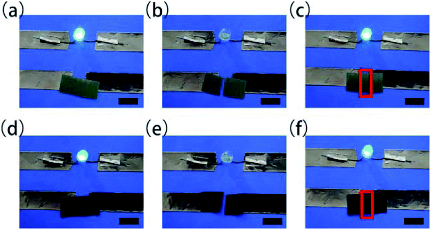 | ||
| Fig. 3 Photographs of the AgNW/TPU film and the AgNW/PDMS film connected to a circuit with an LED bulb. (a–c) As-prepared AgNW/TPU film in the circuit before and after healing. (d–f) As-prepared AgNW/PDMS film in the circuit before and after healing. Scale bars, 10 mm. | ||
A time-controlled experiment illustrated the healing process in Fig. 4, which shows the optical microscopy images of the healing samples under NIR irradiation. The scratched TPU film is shown in Fig. 4a. Then, the ends of the fracture were contacted as close as possible (Fig. 4b). Under NIR light irradiation, the length and width of the scratches gradually decreased, and the region was healed to about 70% of the original area in 15 min (Fig. 4c). The optical microscopy images show that some scratches in the samples had completely disappeared (according to visual observation) with 30 min NIR light irradiation (Fig. 4d). The healing of TPU is a result of the thermal effect of the NIR lamp, but excessive irradiation could cause the embedded AgNWs to submerge in the TPU, which increases the resistance of the conductive side of the TPU film. The other scratches on the PDMS film are displayed in Fig. 4e. After 30 min of exposure to NIR light, the scratches completely healed, which was observed under the microscope (Fig. 4h). The results show that the healing process is induced by NIR light. With the driving force of thermal energy on the molecular mobility, the TPU film heated above the Tm melted to heal and PDMS reconnected the hydrogen bonds.42,43 However, healing was only possible when the crosslinks were photo-induced instead of just being heated, especially for PDMS, which has a higher melting point.37,44 The healing process of the films demonstrates the recombination of the chemical bonds in the cross-linking networks in response to temperature and light stimuli.45,46
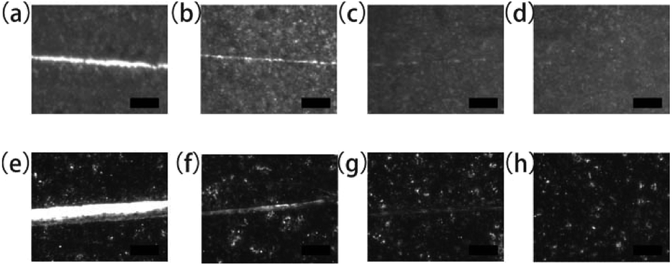 | ||
| Fig. 4 The healing process of an AgNW/TPU film and an AgNW/PDMS film. (a) Scratching TPU film. (b) Contacting the ends of the fracture. (c) Under the NIR light irradiation, the scratches gradually decreased. (d) The scratches fully healed. (e) Scratching PDMS film. (f) Contacting the ends of the fracture. (g) The scratches gradually decreased under the NIR light irradiation. (h) The scratches fully healed. Scale bars, 1 mm. | ||
Performance characterization of the self-healing TENG
The electrical performance of the fabricated SH-TENG was carefully tested, and the triboelectric series of different materials was studied (Fig. S9 and S10†).47 As shown in Fig. 5a, the TENG was fabricated by integrating the embedded AgNWs in a dielectric layer of TPU and PDMS with the whole thickness of ∼220 μm. TPU was utilized as the triboelectrically positive material, and PDMS was utilized as the triboelectrically negative material. The images of the fabricated parts of the SH-TENG are displayed in Fig. 5b and c. A copper wire was connected to the AgNW electrode using transparent tape for electrical measurements. Finally, the TPU and PDMS contacted face to face to form the SH-TENG. The operation principle of the SH-TENG is based on the contact-separation mode,48,49 which is schematically depicted in Fig. 5d. When a mechanical force is applied to SH-TENG, charges are produced and transferred from the surface of the TPU layer to the PDMS layer, generating equivalent negative and positive charges on both surfaces. When separated by releasing the external force, electrons are transferred from the PDMS layer to the TPU layer due to their different potentials. This electric current stops flowing when it reaches electrostatic equilibrium. Therefore, AC electricity can be continuously generated by the periodical contact-separation between the insulating layer and bottom electrode.50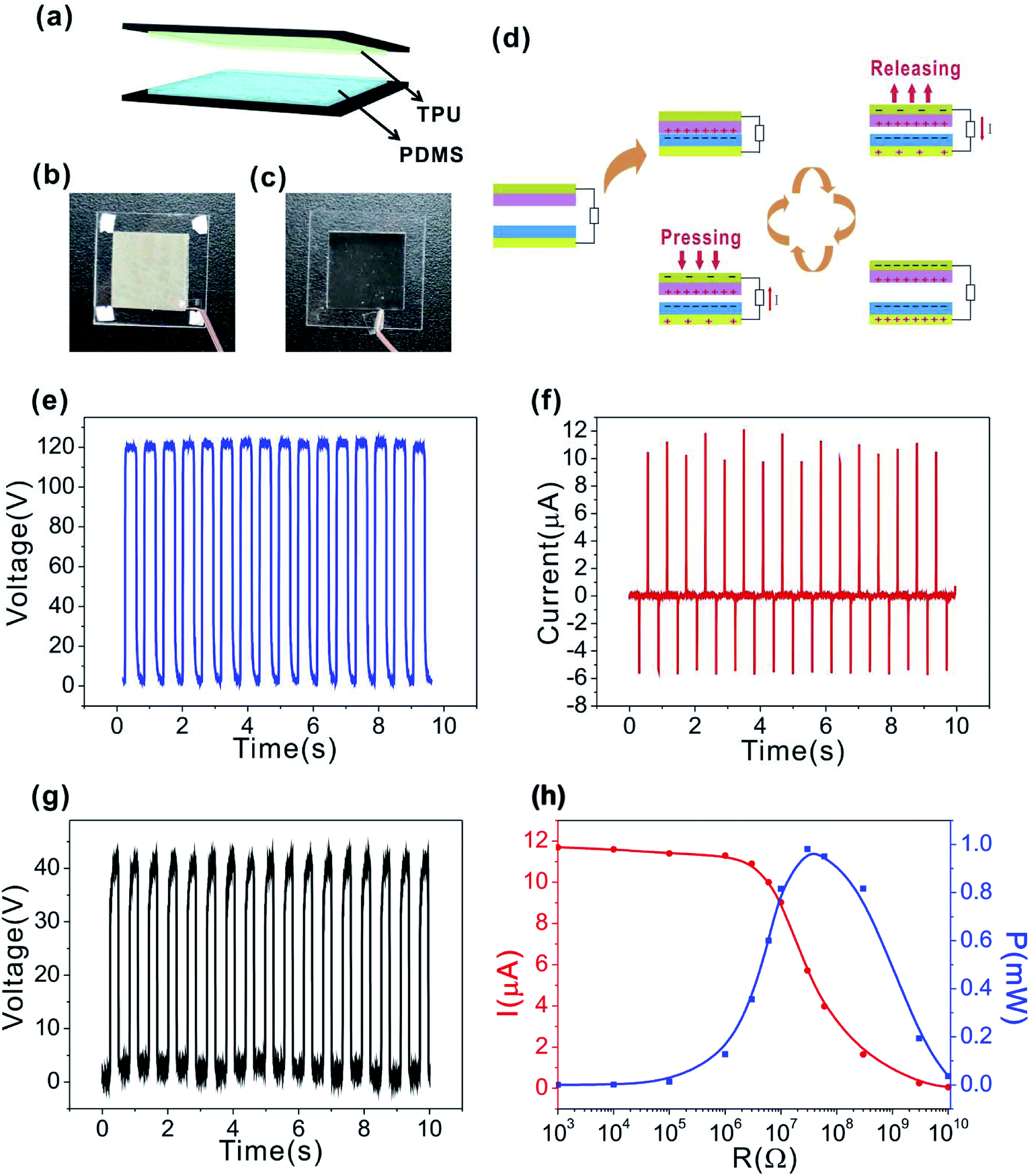 | ||
| Fig. 5 Structure and performance of the TENG for harvesting mechanical energy. (a) Schematic diagram of the experiment setup. (b and c) Photographs of the TPU and PDMS films. (d) Working principle of the TENG. (e–h) Performance characterization of the TENG. (e) Open-circuit voltage, (f) short-circuit current, (g) transferred charge number and (h) dependence of the current and instantaneous power on the external resistance load. (The triboelectric surface between TPU and PDMS is 2 cm × 2 cm.) | ||
Detailed electrical characterizations were carried out to investigate the output performance of the SH-TENG. The open-circuit voltage and short-circuit current of the SH-TENG were measured using a Keithley 6514 electrometer. Unless otherwise specified, the sizes of the SH-TENG used in this work were all 2 cm × 2 cm. Also, a Voc of 120 V and Isc of 11.6 μA were obtained by applying a stable driving force (Fig. 5e and f), respectively. The compressive force was approximately 5 N. The peak value of Isc corresponded to the process of pressing, and the positive voltage was generated because of the immediate charge separation. The voltage was maintained at a plateau until the subsequent pressing. Here, the amount of transferred charges (Q) is about 40 nC (Fig. 5g) and the triboelectric charge density is 100 μC m−2. In fact, the effective output power of the TENG depends on the external load. Fig. 5h shows the dependence of the current on the external load resistance, which varies from 1 kΩ to 10 GΩ. It is clearly seen that as the resistance increased, the current amplitude decreased. The instantaneous power relied on the load of the TENG, as shown in Fig. 5h. This was calculated using expression 1.
| P = I2R | (1) |
The instantaneous power exhibits a maximum value of about 1 mW at a resistance load of 60 MΩ, and the corresponding power density of the TENG is about 2.5 W m−2. During the process of harvesting mechanical energy, TENG have to be constantly operated for a long term under massive and complex mechanical impacts, which causes breakdown and performance degradation in the device. However, owing to the self-healing functions of the polymer materials and AgNW electrode, the as-prepared TENG is recoverable. Most importantly, the excellent self-healing capability of the as-prepared TENG is observed in its output performance.
We evaluate three primary parameters of SH-TENG (Fig. 6a, b and 6c), including Isc, Voc and Q, on the self-healing performance of the device, respectively. For one typical sample tested under a certain mechanical force, the results show Voc of 120 V, Isc of 11.6 μA and Q of 40 nC can be generated by the original device. Although both the applied impulse and the device dimension remain unchanged when the SH-TENG was cut into two fragments, the Voc, Isc and Q decreased to about 70 V, 6 μA and 20 nC, respectively. Such an obvious change in output performance may be attributed to the variation in the effective contact area between TPU and PDMS before and after cutting. Once the broken ends connected for self-healing, the Voc, Isc and Q were restored and approached the initial performance, which achieved the high healing efficiency of 99%. To further evaluate the repeatability of the healing process, we measured the electric output of the as-fabricated TENG after 5 cutting/healing cycles. The results show that the healed device still effectively worked with a negligible decrease in its performance (Fig. 6d), indicating the great recoverability of SH-TENG for converting mechanical energy into electricity with a prolonged lifespan, durability and robustness. In this regard, the self-healing and flexible SH-TENG possesses distinct advantages for practical applications. The SH-TENG shows the potential to adapt to complex mechanical stimuli when serving as an energy harvester and self-powered sensor for various motions.
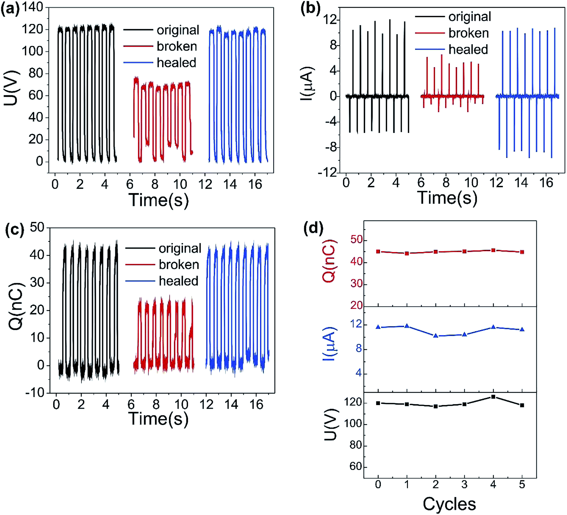 | ||
| Fig. 6 Self-healing process illustrated by the electric output performance of the SH-TENG (a–c). Open-circuit voltage (a) short-circuit current (b) and transferred charges (c) of the self-healing TENG in the original, broken, and healed states. (d) Electric stability of the SH-TENG when subjected to repetitive cutting/healing cycles. | ||
Experimental
Preparation of PDMS and TPU films
![[thin space (1/6-em)]](https://www.rsc.org/images/entities/char_2009.gif) :1 by weight. A certain amount of graphite powder (GP) was added through simple mechanical mixing. After the air bubbles disappeared, we obtained a liquid mixture. As shown in Fig. 1, the AgNW solution was uniformly casted on a photographic paper substrate with a rectangle-shaped area (7 cm × 4 cm) patterned with Kapton tape (25 μm). Photographic paper ensured the smoothness of the silver nanowire film, and the PDMS film could be easily peeled off from the photographic paper for further preparation of the device. The AgNW film was dried for 1 h in air at room temperature (Fig. 1a). The upper thin PDMS layer was prepared by the glass rod coating method. A liquid mixture of PDMS and GP was poured and bar-coated onto the AgNW film back and forth to obtain a smooth PDMS layer (Fig. 1c). Then, the tape was removed from the substrate. Subsequently, the whole piece was cured at 70 °C for 2 h to form solid PDMS (Fig. 1e). Then the film was peeled off from the photographic paper substrate (Fig. 1g). Consequently, the bottom surfaces of the PDMS were symmetrically covered by the AgNW electrodes.
:1 by weight. A certain amount of graphite powder (GP) was added through simple mechanical mixing. After the air bubbles disappeared, we obtained a liquid mixture. As shown in Fig. 1, the AgNW solution was uniformly casted on a photographic paper substrate with a rectangle-shaped area (7 cm × 4 cm) patterned with Kapton tape (25 μm). Photographic paper ensured the smoothness of the silver nanowire film, and the PDMS film could be easily peeled off from the photographic paper for further preparation of the device. The AgNW film was dried for 1 h in air at room temperature (Fig. 1a). The upper thin PDMS layer was prepared by the glass rod coating method. A liquid mixture of PDMS and GP was poured and bar-coated onto the AgNW film back and forth to obtain a smooth PDMS layer (Fig. 1c). Then, the tape was removed from the substrate. Subsequently, the whole piece was cured at 70 °C for 2 h to form solid PDMS (Fig. 1e). Then the film was peeled off from the photographic paper substrate (Fig. 1g). Consequently, the bottom surfaces of the PDMS were symmetrically covered by the AgNW electrodes.Fabrication of the SH-TENG
A 2 mm-thick acrylic sheet was cut into a 3 cm × 3 cm square using a laser cutter (Universal PLS6.75) as a supporting substrate. Foam tape with a thickness of 1 mm was used as the buffer layer to provide the soft contact. The PDMS film and TPU film were cut 2 cm × 2 cm in size and then attached to the acrylic support. The enameled Cu wires were used to connect the AgNW electrodes to the measurement system.Characterization and measurement
The nanostructures on the surface of the AgNW-embedded PDMS and TPU electrodes were observed by field-emission scanning electron microscopy (SEM, HITACHI, SU8020). To test the electric output of the SH-TENG, a linear motor (Linmot E1100) was applied to mimic motions, which drove the TENG contact and separation. A programmable electrometer (Keithley 6514) was adopted to test the open-circuit voltage, short-circuit current, and transferred charge. The software platform was constructed based on LabVIEW, which is capable of realizing real-time data acquisition control and analysis.Conclusions
In summary, we fabricated a high-performance, flexible triboelectric nanogenerator with reproducible self-healing electronic characteristics by embedding electrically and thermally conductive AgNWs in TPU and PDMS films. Based on the soft and flexible polymers, the SH-TENG achieved a peak power of 2.5 W m−2 and triboelectric charge density of 100 μC m−2. By integrating AgNWs in the polymer layers, these films could effectively and rapidly restore from the breakage caused by cuts and scratches under NIR light irradiation. Also, repetitive cutting/healing processes at the same region were demonstrated without significant decline in the electrical performance of the SH-TENG. Furthermore, both output voltage and current of the healed device reached up to about 99% of their original values even after five cutting/healing cycles. These films can act as promising self-healing materials and are believed to have potential applications in flexible electronic devices with prolonged durability and reliability.Conflicts of interest
There are no conflicts to declare.Acknowledgements
This work is supported by the Beijing Natural Science Foundation (No. 2182014), the National Natural Science Foundation of China (NSFC No. 21703010, 51503005 and 21274006), National Key R&D Project from Minister of Science and Technology (2016YFA0202702, 2016YFA0202703, and 2016YFA0202704), the Programs for Beijing Science and Technology Leading Talent (Grant No. Z161100004916168), the Beijing Hundred, Thousand and Ten Thousand Talent Project (110403000402), the Fundamental Research Funds for the Central Universities, the “Thousands Talents” Program for Pioneer Researcher and His Innovation Team, China, the National Postdoctoral Program for Innovative Talents and the General Financial Grant from the China Postdoctoral Science Foundation (Grant No. BX201700061 and 2017M620710).Notes and references
- X. Cheng, Z. Yunlong, W. A. Chi, Z. Haiyang, D. Yejing, H. Xu, W. Peihong, W. Yi-Cheng, F. Peizhong, L. Dawei and W. Z. Lin, Adv. Mater., 2018, 30, 1706790 CrossRef PubMed.
- K. Dong, J. Deng, W. Ding, A. C. Wang, P. Wang, C. Cheng, Y.-C. Wang, L. Jin, B. Gu, B. Sun and Z. L. Wang, Adv. Energy Mater., 2018, 8, 1801114 CrossRef.
- Y. Wang, J. Duan, Y. Zhao, Y. Duan and Q. Tang, Nano Energy, 2017, 41, 293–300 CrossRef.
- J. Kim, J. H. Lee, H. Ryu, J. H. Lee, U. Khan, H. Kim, S. S. Kwak and S. W. Kim, Adv. Funct. Mater., 2017, 27, 8 Search PubMed.
- X. Zhao, Z. Kang, Q. L. Liao, Z. Zhang, M. Y. Ma, Q. Zhang and Y. Zhang, Nano Energy, 2018, 48, 312–319 CrossRef.
- Y. Lee, S. H. Cha, Y.-W. Kim, D. Choi and J.-Y. Sun, Nat. Commun., 2018, 9, 1804 CrossRef PubMed.
- S. Wang, L. Lin and Z. L. Wang, Nano Lett., 2012, 12, 6339–6346 CrossRef PubMed.
- Q. Tang, M.-H. Yeh, G. Liu, S. Li, J. Chen, Y. Bai, L. Feng, M. Lai, K.-C. Ho, H. Guo and C. Hu, Nano Energy, 2018, 47, 74–80 CrossRef.
- Q. Zhang, Q. J. Liang, Z. Zhang, Z. Kang, Q. L. Liao, Y. Ding, M. Y. Ma, F. F. Gao, X. Zhao and Y. Zhang, Adv. Funct. Mater., 2018, 28, 8 Search PubMed.
- S. H. Sung, Y. S. Kim, D. J. Joe, B. H. Mun, B. K. You, D. H. Keum, S. K. Hahn, M. Berggren, D. Kim and K. J. Lee, Nano Energy, 2018, 51, 102–112 CrossRef.
- Z. Yuan, T. Zhou, Y. Yin, R. Cao, C. Li and Z. L. Wang, ACS Nano, 2017, 11, 8364–8369 CrossRef PubMed.
- U. Khan, T. H. Kim, H. Ryu, W. Seung and S. W. Kim, Adv. Mater., 2017, 29, 8 Search PubMed.
- W. Yang, N.-W. Li, S. Zhao, Z. Yuan, J. Wang, X. Du, B. Wang, R. Cao, X. Li, W. Xu, Z. L. Wang and C. Li, Adv. Mater. Technol., 2018, 3, 1700241 CrossRef.
- X. Du, N. Li, Y. Liu, J. Wang, Z. Yuan, Y. Yin, R. Cao, S. Zhao, B. Wang, Z. L. Wang and C. Li, Nano Res., 2018, 11, 2862–2871 CrossRef.
- H. Guo, M. H. Yeh, Y. C. Lai, Y. Zi, C. Wu, Z. Wen, C. Hu and Z. L. Wang, ACS Nano, 2016, 10, 10580–10588 CrossRef PubMed.
- X. Cheng, L. Miao, Y. Song, Z. Su, H. Chen, X. Chen, J. Zhang and H. Zhang, Nano Energy, 2017, 38, 438–446 CrossRef.
- C. Li, Y. Yin, B. Wang, T. Zhou, J. Wang, J. Luo, W. Tang, R. Cao, Z. Yuan, N. Li, X. Du, C. Wang, S. Zhao, Y. Liu and Z. L. Wang, ACS Nano, 2017, 11, 10439–10445 CrossRef PubMed.
- R. Cao, T. Zhou, B. Wang, Y. Yin, Z. Yuan, C. Li and Z. L. Wang, ACS Nano, 2017, 11, 8370–8378 CrossRef PubMed.
- Y. Liu, X. Du, J. Wang, Y. Yin, B. Wang, S. Zhao, N. Li and C. Li, J. Hazard. Mater., 2018, 347, 25–30 CrossRef PubMed.
- R. Cao, J. Wang, S. Zhao, W. Yang, Z. Yuan, Y. Yin, X. Du, N.-W. Li, X. Zhang, X. Li, Z. L. Wang and C. Li, Nano Res., 2018, 11, 3771–3779 CrossRef.
- K. Parida, V. Kumar, W. Jiangxin, V. Bhavanasi, R. Bendi and P. S. Lee, Adv. Mater., 2017, 29, 1702181 CrossRef PubMed.
- J. Deng, X. Kuang, R. Liu, W. Ding, A. C. Wang, Y. C. Lai, K. Dong, Z. Wen, Y. Wang, L. Wang, H. J. Qi, T. Zhang and Z. L. Wang, Adv. Mater., 2018, 30, e1705918 CrossRef PubMed.
- L. B. Huang, G. Bai, M. C. Wong, Z. Yang, W. Xu and J. Hao, Adv. Mater., 2016, 28, 2744–2751 CrossRef PubMed.
- V. K. Thakur and M. R. Kessler, Polymer, 2015, 69, 369–383 CrossRef.
- W. Xu, L.-B. Huang and J. Hao, Nano Energy, 2017, 40, 399–407 CrossRef.
- S. Cheon, H. Kang, H. Kim, Y. Son, J. Y. Lee, H.-J. Shin, S.-W. Kim and J. H. Cho, Adv. Funct. Mater., 2018, 28, 1703778 CrossRef.
- J. Wang, C. Wu, Y. Dai, Z. Zhao, A. Wang, T. Zhang and Z. L. Wang, Nat. Commun., 2017, 8, 88 CrossRef PubMed.
- C. Wang, H. Wu, Z. Chen, M. T. McDowell, Y. Cui and Z. Bao, Nat. Chem., 2013, 5, 1042–1048 CrossRef PubMed.
- L. Hu, H. S. Kim, J.-Y. Lee, P. Peumans and Y. Cui, ACS Nano, 2010, 4, 2955–2963 CrossRef PubMed.
- Y. Joo, J. Byun, N. Seong, J. Ha, H. Kim, S. Kim, T. Kim, H. Im, D. Kim and Y. Hong, Nanoscale, 2015, 7, 6208–6215 RSC.
- H. Fan, K. Li, Q. Li, C. Hou, Q. Zhang, Y. Li, W. Jin and H. Wang, J. Mater. Chem. C, 2017, 5, 9778–9785 RSC.
- L. Lu, X. Wei, Y. Zhang, G. Zheng, K. Dai, C. Liu and C. Shen, J. Mater. Chem. C, 2017, 5, 7035–7042 RSC.
- F. Xu and Y. Zhu, Adv. Mater., 2012, 24, 5117–5122 CrossRef PubMed.
- Y. Li, S. Chen, M. Wu and J. Sun, ACS Appl. Mater. Interfaces, 2014, 6, 16409–16415 CrossRef PubMed.
- M.-K. Kim, M.-S. Kim, H.-B. Kwon, S.-E. Jo and Y.-J. Kim, RSC Adv., 2017, 7, 48368–48373 RSC.
- L. Huang, N. Yi, Y. Wu, Y. Zhang, Q. Zhang, Y. Huang, Y. Ma and Y. Chen, Adv. Mater., 2013, 25, 2224–2228 CrossRef PubMed.
- S. Wang, N. Liu, J. Su, L. Li, F. Long, Z. Zou, X. Jiang and Y. Gao, ACS Nano, 2017, 11, 2066–2074 CrossRef PubMed.
- Y. Sun, J. Lopez, H. W. Lee, N. Liu, G. Zheng, C. L. Wu, J. Sun, W. Liu, J. W. Chung, Z. Bao and Y. Cui, Adv. Mater., 2016, 28, 2455–2461 CrossRef PubMed.
- S. H. Jeong, S. Zhang, K. Hjort, J. Hilborn and Z. Wu, Adv. Mater., 2016, 28, 5830–5836 CrossRef PubMed.
- L. Liu, S. Liang, Y. Huang, C. Hu and J. Yang, Chem. Commun., 2017, 53, 12088–12091 RSC.
- Q. Rong, W. Lei, L. Chen, Y. Yin, J. Zhou and M. Liu, Angew. Chem., Int. Ed. Engl., 2017, 56, 14159–14163 CrossRef PubMed.
- B. Zhang, P. Zhang, H. Zhang, C. Yan, Z. Zheng, B. Wu and Y. Yu, Macromol. Rapid Commun., 2017, 38, 1700110 CrossRef PubMed.
- J. H. Lee, R. Hinchet, S. K. Kim, S. Kim and S.-W. Kim, Energy Environ. Sci., 2015, 8, 3605–3613 RSC.
- Y. Yang and M. W. Urban, Chem. Soc. Rev., 2013, 42, 7446–7467 RSC.
- J. Zhao, R. Xu, G. Luo, J. Wu and H. Xia, Polym. Chem., 2016, 7, 7278–7286 RSC.
- M. W. Keller, S. R. White and N. R. Sottos, Adv. Funct. Mater., 2007, 17, 2399–2404 CrossRef.
- Z. L. Wang, ACS Nano, 2013, 7, 9533–9557 CrossRef PubMed.
- J. W. Lee, H. J. Cho, J. Chun, K. N. Kim, S. Kim, C. W. Ahn, I. W. Kim, J. Y. Kim, S. W. Kim, C. Yang and J. M. Baik, Sci. Adv., 2017, 3, 9 Search PubMed.
- X. Wang, S. Niu, F. Yi, Y. Yin, C. Hao, K. Dai, Y. Zhang, Z. You and Z. L. Wang, ACS Nano, 2017, 11, 1728–1735 CrossRef PubMed.
- J. Wang, Z. Wen, Y. Zi, P. Zhou, J. Lin, H. Guo, Y. Xu and Z. L. Wang, Adv. Funct. Mater., 2016, 26, 1070–1076 CrossRef.
Footnotes |
| † Electronic supplementary information (ESI) available. See DOI: 10.1039/c8ra05305g |
| ‡ H. Niu, X. Du and S. Zhao contributed equally to this work. |
| This journal is © The Royal Society of Chemistry 2018 |