
 Open Access Article
 This Open Access Article is licensed under a Creative Commons Attribution-Non Commercial 3.0 Unported Licence
Effects of stacking method and strain on the electronic properties of the few-layer group-IVA monochalcogenide heterojunctions†
Yonghong Hu‡
 *a,
Caixia Mao‡a,
Zhong Yanb,
Ting Shua,
Hao Nia,
Li Xuea and
Yunyi Wuc
*a,
Caixia Mao‡a,
Zhong Yanb,
Ting Shua,
Hao Nia,
Li Xuea and
Yunyi Wuc
aSchool of Nuclear Technology and Chemistry & Biology, Hubei University of Science and Technology, Xianning 437100, China. E-mail: hchyh2001@tom.com; Tel: +86-0715-8263712
bCollege of Material Science and Engineering, Nanjing University of Science and Technology, Nanjing 210094, China
cDepartment of Electrical Engineering, The Hong Kong Polytechnic University, Hung Hom, Kowloon, Hong Kong
First published on 23rd August 2018
Abstract
Group-IV monochalcogenides (GeSe, SnSe, GeS, SnS) are a class of promising monolayer materials for nanoelectronic applications. However, the GeSe monolayer is the only direct semiconductor in the group-IV monochalcogenides, which limits their application in nanoelectronic fields. Stacking is usually a good strategy to design two-dimensional (2D) materials with novel properties. Taking these monolayer monochalcogenides as basic building blocks, various van der Waals (vdW) heterojunctions can be constructed by different stacking methods. In this study, we systematically investigated the structures, stabilities and electronic properties of thirty-six few-layer group-IV monochalcogenide heterojunctions. All the vdW heterojunctions are proved to be stable. The degree of stability of the few-layer heterojunctions is found to increase with the number of layers. The band gap values of heterojunctions are dependent not only on the components, but also on the stacking order. Five novel 2D direct semiconductors (SnSe/GeSe, GeS/SnS, SnSe/GeSe/SnSe, SnS/GeSe/SnSe and SnS/GeSe/SnSe) are obtained. It's found that biaxial strain can not only tune the values of band gap, but also change the type of the 2D materials. The band gaps of the heterojunctions monotonically increase with the increasing strain and most few-layer heterojunctions transform between direct and indirect semiconductors under biaxial strain. Five heterojunctions (SnSe/GeSe, GeS/SnS, GeSe/SnSe/SnS, SnS/GeSe/SnSe and GeSe/SnS/GeS/SnSe) are found to remain as direct semiconductors under tensile strain (0–0.1). Since the band gaps of these heterojunctions are easy to control in a suitable range, they may have potential applications in nanoelectronic fields.
Introduction
The discovery and application of graphene inspired the upsurge of 2D materials research,1 and have played a revolutionary role in the scientific community with extraordinary electronical, mechanical and optical properties.2,3 Other 2D materials, such as boron nitride, molybdenum disulfide, black phosphorus, etc., have further attracted a wide range of research interests in the fields of physics, chemistry and material science.4–6 The zero band gap of graphene, the low carrier mobility of molybdenum disulfide and the instability of black phosphorus in air limit their practical applications in nanoelectronic devices.7–10 Therefore, it is of great importance to find new 2D materials with unique physical and chemical properties, which are suitable for new applications in nanoelectronic devices.Due to its high stability, low toxicity and similar structure to black phosphorus,11–13 group-IV monochalcogenides (GeS, GeSe, SnS and SnSe) have gained increasing attention and shown excellent optoelectronic properties.14–22 Among the four monochalcogenides, only GeSe exhibits a direct band gap.21 According to the report of Zhang et al., GeSe monolayer has five different configurations: α-GeSe, β-GeSe, γ-GeSe, δ-GeSe and ε-GeSe.22 Various GeSe nanosheets have been synthesized by different methods, which are promising materials in photodetector devices.14–19 Mukherjee et al. fabricated high-quality GeSe single crystal nanosheets using chemical vapor deposition technologies, and produced a Schottky photodetector based on those with high optical flow gain.17 Under high pressure and high temperature conditions, the electrical conductivity of GeSe is higher than both black phosphorus and graphene.23 All the 2D GeSe configurations are classified into two different phases, i.e. black-phase and blue-phase.24–27 Theoretical research results of Ji et al. showed that the work function of the black-phase GeSe doesn't meet the oxidation potential of O2/H2O, while the blue-phase GeSe is a suitable photocatalyst for water splitting.28 Recently, Mao et al. have fabricated single-layer GeSe crystal using mechanical stripping and laser thinning techniques.29 Photoluminescence experiments showed that monolayer GeSe has potential application in solar cell due to its proper absorption peak range.30
Stacking of 2D materials has become a popular and effective method for designing new 2D materials. For example, bilayer phosphorene and MoS2 exhibit more striking properties than a single layer sheet.31,32 vdW heterostructures with two types of 2D materials seem to be a magic way to break through the limitations of single 2D materials. For example, 2D SiGe/h-BN vdW heterojunction exhibits inspired electronic and optical properties.33 Previously, we reported on the stability and electronic properties of single-layer GeSe (direct bandgap and small carrier effective mass),21 and stimulated the researcher's attentions to the 2D group-IV monochalcogenides materials.34–40 For example, Shi et al. studied the anisotropic spin transport properties and strong visible light absorption of few-layer GeSe and SnSe.34 Hao et al. predicted theoretically that vacancy doped few-layer GeSe has high thermoelectric properties.35 Fan et al. performed theoretical studies on the electronic structures of GeSe nanobelts and nanosheets.36 Sun et al. fabricated 2D SnSe/GeSe heterojunction nanosheets by solution method.37 Wang et al. predicted that few-layer GeSe has potential applications in near-infrared short wave polarization detectors.38 Xue et al. produced high quality GeSe single crystal films and found their important applications in solar cells.39 Kamal et al. investigated the electronic structures of group-IV monochalcogenides by first-principles calculations and predicted their prospects in light-emitting diodes and solar cells.40 In addition, there may exist two types of 2D heterostructures due to the reduced dimensionality, namely, vertical heterostructure (vdW interaction) and lateral (in-plane) heterostructure. Compared to vertical heterostructures, the lateral heterostructures have many virtues, such as simpler band alignment, less interface region, more distinct phase separation etc41. 2D lateral heterostructure attracted great interests of theoretical and experimental researchers.42–47 Recently, Zhao et al. studied the band alignment and electronic properties of lateral heterosturctures of monolayer group-IV monochalcogenides and reported their potential application in high-efficiency solar cell.47
In the present work, we designed a group of few layered 2D vertical heterojunctions composed of group-IV monochalcogenides monolayers, namely, 2D GeS, GeSe, SnS and SnSe configurations. Through first-principle calculations, the geometric structure, stability and electronic properties are systematically investigated from a theoretical point of view. The vdW interactions of the monolayers are weak. Therefore the linear band gap dispersion state is not perturbed in the heterojunctions. The geometric structure, stability and electronic properties of 2D few-layer heterojunctions are calculated and analyzed. The band gaps of these few-layer heterojunctions are dependent on both their stacking order and components. Moreover, an impressive decrease of band gap in the few-layer heterojunctions is found, and the values of band gap are tunable under biaxial strain.
Computational method
The first principle calculations were conducted with the CASTEP48 quantum mechanics program in the Materials Studio 8.0 package. The ultrasoft pseudopotential49 was employed to simulate the interactions between ions and electrons. The generalized gradient approximation (GGA) Perdew–Burke–Ernzerhof (PBE) functionalization50–52 was used to handle the exchange–correlation interaction of electrons. In order to describe the influence of the inter-layer vdW interactions accurately, Tkatchenko–Scheffler (TS) vdW functional theory was applied. The double-layer structure allows various superposition orders (AA, AB, AC, and AD stacking) due to weak inter-layer vdW interactions,34,53,54 where the bilayer structure obtained by AA stacking is the most stable.30 In this study, the group-IV monochalcogenides monolayers, namely, 2D GeS, GeSe, SnS and SnSe, all have an orthorhombic structure, as reported in our previous publication.21 Taking these four monolayers as basic building blocks, we have constructed six bilayer, thirteen trilayer and twelve four-layer heterojunctions with AA stacking method. The thirty-six few-layer heterojunctions were designed through stacking in the (001) direction. These vdW heterojunction models were periodic and the lattice parameters of these group-IV monochalcogenides monolayers in the direction of the heterojunction interface are compatible.53 A sufficient large vacuum layer (25 Å, 35 Å and 45 Å for bilayer, trilayer and four-layer 2D heterojunctions, respectively) was retained in the heterostructure to ensure that the interaction of the heterojunction and its mirror system was eliminated. The Brillouin zone was sampled by the Monkhorst–Pack method45 and it was divided into 13 × 13 × 1 lattices. In order to calculate the specific k-points and optimize the geometry of the system. The specific parameters are designed as follows: the energy deviation is less than 5.0 × 10⁻⁶ eV per atom, the force on each atom is less than 0.01 eV Å−1, and the maximum stress deviation is less than 0.02 GPa, the maximum displacement deviation is less than 5.0 × 10⁻⁴ Å. Through the energy convergence test, the plane wave cutoff can be set to 500 eV, the accuracy of the electronic self-consistent field calculation (SCF) is set to 5.0 × 10⁻⁷ eV per atom. The PBE approximation approximates the band structure of the thirty-three heterojunction models. The binding energy is defined as , where Etotal is the total binding energy, n is the number of monolayers in the heterojunction system and Emonoi is the ith monolayer which constitutes the heterojunction. In-plane biaxial strain is defined as ε = (a − a0)/a = (b − b0)/b, where a0 and b0 are the lattice constants of the studied vdW heterojunction, respectively. Correspondingly, a and b are the lattice constants along the x and z directions under biaxial strain.
Results and discussion
Geometric structure and stability
After fully relaxation, the crystal structures of the six bilayer heterojunctions are shown in Fig. 1. The corresponding values of lattice constants, average bond length, mismatch of lattice constants, binding energy, and band gap are listed in Table 1. For comparison, the lattice constants, the average bond lengths, and the band gap values of the four group-IV monochalcogenides monolayer are also calculated and listed in Table S1 in the ESI,† which are in agreement with our previous results.21 As seen from Fig. 1(a) and (b), each monolayer in the GeSe/GeS and SnSe/GeSe heterojunctions retain black-phase structure after geometry optimization due to their small lattice mismatches and suitable interlayer distances. Comparing the values of average bond-length in Tables 1 and S1,† it's found that the average bond-lengths in the six heterostructures are all approximately equal to those in the two monolayers included in the corresponding heterojunction. Furthermore, the average bond length in GeSe/GeS heterojunction is the closest to those in the GeS and GeSe monolayers. From Fig. 1(c), (d) and (f), it's found that the SnS monolayers in SnS/GeSe, GeS/SnS and SnS/SnSe heterojunctions have undergone severe deformation, and the chemical bond breaks in the SnS monolayer. From Fig. 1(e) and (f), it's found that the SnSe monolayers in GeS/SnSe and SnS/SnSe heterojunctions also have undergone obvious deformation and chemical bond breakage. As shown in Fig. 1(f), the geometry deformation in SnSe/SnS heterojunction is the most obvious, because both SnS and SnSe monolayers have changed the original black-phase configurations. As shown in Table 1, the maximum lattice mismatches of GeS/SnS and SnS/SnSe heterojunctions are larger than 5%, which may be the main reason causing the geometry deformations. And the geometry deformations in SnS/GeSe and SnS/SnSe heterojunctions may be in close relationship with the distances between the two monolayers in the heterojunctions, as these two distances are significantly larger than that normal distance corresponding to usual vdW heterojunction (3 Å).55–59 To examine the stability of the six bilayer heterojunctions, we calculated their binding energies (the results are shown in Table 1). From Table 1, it can be seen that their binding energies are all negative, showing that they all have good stability. Comparing the values of binding energies of bilayer GeSe with different stacking order (−52.3, −48.1, −30.3 and −37.5 meV for the four type configurations, respectively),30 it can be concluded that our calculation results are reliable and the GeSe/GeS, SnSe/GeSe and SnS/SnSe heterojunctions are more stable than the other three heterojunctions. | ||
| Fig. 1 Optimized crystal structure of the six vdW heterojunctions. Among them, yellow, green, orange, and gray balls represent S, Ge, Se, and Sn atoms, respectively. | ||
![[l with combining macron]](https://www.rsc.org/images/entities/i_char_006c_0304.gif) ), distance between the two monolayers (d), binding energy (Eb), and band gap (Eg) of the vdW heterojunction crystals of group-IVA monochalcogenides. In the table, “I” represent indirect gap, and “D”represents direct gap
), distance between the two monolayers (d), binding energy (Eb), and band gap (Eg) of the vdW heterojunction crystals of group-IVA monochalcogenides. In the table, “I” represent indirect gap, and “D”represents direct gap
| Models | a (Å) | b (Å) | χ | (Å) |
d (Å) | Eb (eV) | Eg (eV) |
|---|---|---|---|---|---|---|---|
| GeSe/GeS | 3.87 | 4.07 | 4.2% | 2.52 | 3.14 | −49 | 0.85 I |
| SnSe/GeSe | 4.10 | 4.25 | 3.2% | 2.71 | 3.21 | −46 | 0.29 D |
| SnS/GeSe | 4.03 | 4.14 | 1.7% | 2.60 | 3.27 | −51 | 0.69 I |
| GeS/SnS | 3.94 | 4.16 | 5.9% | 2.57 | 3.21 | −35 | 0.73 D |
| GeS/SnSe | 4.00 | 4.28 | 7.5% | 2.65 | 3.03 | −33 | 0.64 I |
| SnS/SnSe | 4.19 | 4.23 | 2.2% | 2.74 | 3.29 | −42 | 0.73 I |
The crystal structures of the eighteen trilayer heterojunctions and twelve four-layer heterojunctions comprised of group-IV monochalcogenides monolayer are shown in Fig. S1 and S2.† The corresponding parameters of lattice constants, average bond lengths, the mismatches of lattice constants etc are listed in Tables S2 and S3 in the ESI.† It's found in Fig. S1 and S2† that six trilayer heterojunctions (SnS/GeS/SnS, GeS/SnS/GeS, SnSe/GeS/GeSe, SnSe/GeSe/SnSe, GeSe/SnSe/GeSe, GeSe/GeS/SnS) retain black-phase structure after geometry optimization, but other twelve trilayer heterojunctions and twelve four-layer heterojunctions undergo structural deformations. For some configurations, such as SnS/GeS/SnS and SnSe/GeS/GeSe etc, the stacking styles in the original structures of heterojunctions (AA stacking) are changed after geometry optimization, which is determined by our geometry optimization process based on the lowest energy principle. Comparing the lattice constants in Tables 1 and S1–S3,† it's found that the mismatch rates of lattice constants in the trilayer heterojunctions in our study are less than 4.9%, and those of four-layer heterojunctions are less than 3.6%, both of which are acceptable and able to yield credible simulation results. The average bond lengths in trilayer heterojunctions are in the range from 2.51 Å to 2.76 Å, while those of four-layer heterojunctions are in the range from 2.63 Å to 2.66 Å. This indicates that the average bond length may decrease with the number of layers. The average distances between the monolayers in trilayer heterojunctions are in the range from 2.74 Å to 3.39 Å, and those of four-layer heterojunctions are in the range from 2.98 Å to 3.42 Å. The average distance between the monolayers in few-layer heterojunctions is independent with the components. The values of binding energies of trilayer and four-layer heterojunctions are all negative, showing that they all have good stability. The average values of the binding energies of six bilayer, eighteen trilayer and twelve four-layer heterojunctions are −42.7 meV, −66.1 meV and −69.8 meV respectively, which means that the stability extent increases with the number of layers in heterojunctions due to vdW interactions.
Electronic structures of the heterojunctions
In our previous study, using the GGA PW91 method, the energy band value of GeSe monolayer was calculated and a direct band gap of 1.16 eV was obtained.21 In this work, the band gaps of both monolayer and few-layer group-IV monochalcogenides configurations are calculated by GGA PBE method, which are listed in Tables 1, S1 and S2† respectively. And the corresponding energy band structures of the bilayer, trilayer and four-layer heterojunctions are plotted in Fig. 2, S3 and S4 (in the ESI†) respectively. It can be seen that the band gaps of group-IV monochalcogenides monolayers in Table S1† are consistent with the previous report.21 Comparing the band gap values in Tables S1† and 1, it's found that the band gaps of the heterojunctions are significantly reduced, which are in the range from 0.29 eV to 0.85 eV. For the trilayer and four-layer heterojunctions, the band gaps are also reduced to be in the ranges from zero to less than 1.14 eV and 0.63 eV respectively. This shows that vdW stacking is an effective band regulation method, and this method can be used properly in designing the narrow band gap 2D heterojunction materials. From Tables S1 and S2,† it's found that the band gap values of heterojunctions are dependent with not only the components of the heterojunctions, but also the stacking order of the building blocks. For example, the band gaps of trilayer heterojunctions in Table S2† are all different, since these eighteen heterojunctions have different components. For another example, although the four-layer heterojunctions are composed of the same building blocks, the twelve band gaps of four-layer heterojunctions in Table S3† are different, since the stacking order of the building blocks in these twelve heterojunctions are different. Usually, the band gap calculated from the PBE functional is underestimated, but the variation trend of band gap versus stacking order and component is correct without extra influence.60 | ||
| Fig. 2 Band structure and DOS of six heterojunction materials. The Fermi level is indicated by a dashed line. | ||
As shown in Fig. 2 and Table 1, SnSe/GeSe and GeS/SnS are direct band semiconductors, and the other bilayer heterojunctions are indirect band semiconductors. As for the trilayer and four-layer heterojunctions considered in this study, it's found from Fig. S3, S4, Tables S2 and S3† that three trilayer heterojunctions (SnSe/GeSe/SnSe, SnS/GeSe/SnSe and SnS/GeSe/SnSe) are direct band semiconductors, while the other fifteen trilayer heterojunctions and all the twelve four-layer heterojunctions are indirect semiconductors. As reported in previous studies,20,21 GeSe is the only direct semiconductor in the group-IV monochalcogenides monolayers. Here, five types of novel 2D direct semiconductors are obtained through just stacking these building blocks into vdW heterojunctions. In fact, semiconductors with direct energy gap have higher optical absorption coefficients than those with indirect gap. So they are more appropriate to make optoelectronic devices (light-emitting diodes and photovoltaic cells). Furthermore, although GeS and SnS monolayers are both indirect semiconductors, GeS/SnS heterojunctions is a direct semiconductor, which means that stacking is also a effective method to tune the electronic properties of materials. This provides a new way to design direct semiconductor with suitable band gap value needed in practical applications from vast amount of indirect semiconductors in nature.
To further understand the electronic structure of the vdW heterojunction materials, taking bilayer heterojunctions as examples, we calculated the density of states (DOS) and corresponding partial DOS (PDOS) of the heterojunctions (Fig. 2). As can be seen from the DOS and PDOS in Fig. 2, the total density of states of the conduction and valence bands is dominated by the p orbit near the Fermi surface. We also calculated the decomposition charge densities of the valence band top (VBM) and the conduction band bottom (CBM), as shown in Fig. 3. From Fig. 3, one can find that the charge density of VBM is mainly located around the Se and S atoms. In contrast, CBM is mainly attributed to the contribution of charge densities around the Ge and Sn atoms. These findings on VBM and CBM are consistent with the analysis of PDOS diagrams. For brevity, taking GeSe/GeS as examples, the DOS are projected into different atoms, as is shown in Fig. S5.† It's found that the VBM is mainly contributed by the p orbital of S or Se atoms, and the CBM is mainly contributed by the p orbital of Ge or Sn atoms.
 | ||
| Fig. 3 VBM and CBM of six heterojunctions with an isopotential value of 0.0015 eÅ−3. | ||
In addition, for all the six vdW heterojunctions in our study, the charge density distributions of CBM are similar. However, the charge density of VBM shows different characteristics in the heterojunctions with direct band gaps. As shown in Fig. 3(a), (b), (d) and (f), the VBMs between the upper layer and the lower layer occur no charge density overlap, which is different from the phenomena in Fig. 3(c) and (e). Therefore, interlayers VBM charge density has a crucial influence on the band gap type of heterojunction.30
Strain effect on tuning the electronic structure
As discussed above, the band gap of 2D group-IV monochalcogenides is extended by stacking these monolayers into few-layer vdW heterojunctions with different stacking orders. However, the band gap of 2D group-IV monochalcogenides is not continuously adjustable through just stacking, because the number of stacking orders is a finite natural number for certain heterojunction system. Studies have shown that the in-plane strain can be used to continuously adjust the band gap of bilayer black phosphorus and MoS2.61–63 Therefore, in order to further extend the electronic properties of the group-IV monochalcogenides, we have studied the effect of biaxial strain on the energy band structures of 2D few-layer group-IV monochalcogenides heterojunctions. Strain can be understood as an elastic field applied to materials, which can be used to tune the physical properties of materials.21 Therefore, under different biaxial strain, the geometrical structures of the vdW heterojunctions change due to the interaction between the elastic field and crystalline field, which induces different distributions of electron density in the vdW heterojunctions and then alters their electronic structures. The applied biaxial strain starts from −0.10, with 0.02 as the step difference, successively rises to 0.10. The variations of the band gaps of the six bilayer, seven trilayer and six four-layer 2D group-IV monochalcogenides heterojunctions with biaxial strain are plotted in Fig. 4, S6 and S7† respectively (the detailed electronic properties of the few-layer heterojunctions under different biaxial strains are listed in Tables S4–S6†). | ||
| Fig. 4 Variations of the band gaps of the six 2D group-IVA monochalcogenides heterojunctions with biaxial strain. | ||
It can be seen from Fig. 4 that the band gaps of the six heterojunctions increase with the increase of biaxial strain, which shows that the strain has a significant and continuous effect on the band gap. As shown in Fig. 4, the band gap curve of SnSe/GeSe is obviously different from those of the other five heterojunctions, since it's approximately a straight line in the strain range from −0.04 to 0.10. While the curves corresponding to the other five 2D heterojunctions increase nonlinearly with strain. The analogue results can also be drawn from Fig. S6 and S7† that the band gaps of four trilayer and two four-layer heterojunctions increase linearly with the strain, because the corresponding curves are also approximately straight lines in the strain range from 0.00 to 0.10. Altogether, the band gaps of the all heterojunctions monotonically increase with the strain increase from −0.10 to 0.10, and the continuously adjustable band gap ranges of bilayer, trilayer and four-layer heterojunction are approximately (0–1.23 eV), (0–1.16 eV) and (0–0.95 eV) respectively. Upon compressed biaxial strain (−0.10, 0.00), the band gaps of all heterojunctions change to zero, indicating the transition from semiconductor to metal.
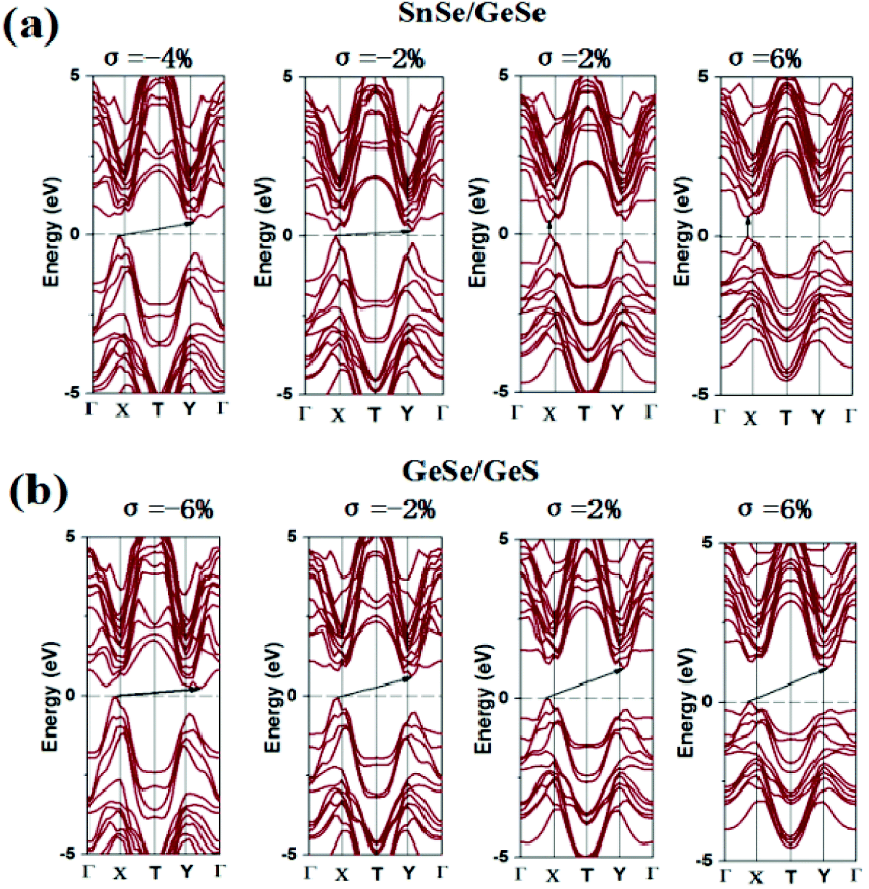
The change of applied strain not only leads to the change of the band gap values, but also usually leads to the transformations of the band gap types of the 2D materials. It is found from Tables S4–S6† that the band gap types of most few-layered heterojunctions considered in our work occur transformations between direct semiconductor and indirect semiconductor except for eight heterojunctions, namely, GeSe/GeS, SnS/SnSe, GeSe/SnSe/SnS, GeSe/GeS/SnS, SnS/GeSe/SnSe, GeS/SnSe/SnS, GeS/GeSe/SnS/SnSe and GeS/GeSe/SnSe/SnS heterojunctions. For brevity, taking SnSe/GeSe and GeSe/GeS vdW heterojunctions as examples, the energy band structures of SnSe/GeSe and GeSe/GeS heterojunctions under several different biaxial strains are plotted in Fig. 5. It can be seen from Fig. 5(a) that SnSe/GeSe heterojunction remains direct semiconductor under tensile strain, but it changes to indirect semiconductor under compressive strain. And when the compressive strain is less than −0.06, SnSe/GeSe heterojunction becomes metallic. It can be seen from Fig. 5(b) that the GeSe/GeS heterojunction remains as an indirect semiconductor whenever under tensile or compressive strain. When the compressive strain is less than −0.08, GeSe/GeS heterojunction becomes metallic.
 | ||
| Fig. 5 Electron band structure of (a) SnSe/GeSe and (b) GeSe/GeS heterojunction under biaxial stress. | ||
It is surprisingly that five few-layer vdW heterojunctions (SnSe/GeSe, GeS/SnS, GeSe/SnSe/SnS, SnS/GeSe/SnSe, GeSe/SnS/GeS/SnSe) are found to remain direct semiconductors under tensile strain, as can be seen in Tables S4–S6 in the ESI.† Through applying tensile biaxial strain, the tunable band-gap range (0–0.92 eV) of these few-layer heterojunctions is slightly wider than that in bilayer phosphorene (0–0.85),63 which shows that these vdW heterojunction materials are also promising for applications in optoelectronics.
Conclusions
In summary, we systematically studied the effect of stacking method and biaxial strain on the electronic properties of the few layered group-IV monochalcogenides heterojunction using the first principles calculation. Our calculations indicate that eight vdW heterojunctions (GeSe/GeS, SnSe/GeSe SnS/GeS/SnS, GeS/SnS/GeS, SnSe/GeS/GeSe, SnSe/GeSe/SnSe, GeSe/SnSe/GeSe, GeSe/GeS/SnS) remain the original black-phase structure after geometry optimization, and the rest twenty-eight few-layer heterojunctions undergo structural deformations, which is due to different stacking method. All the thirty-six vdW heterojunctions have been proved to be stable through considering their negative binding energies. The degree of stability of the few-layer heterojunctions is found to increase with the number of layers in heterojunctions.The band gaps of the few-layer vdW heterojunctions are all significantly reduced compared with their monolayers. Therefore, we conclude that vdW stacking is an effective band regulation method, and this method can be used properly in designing the narrow band gap 2D heterojunction materials. Five novel 2D direct semiconductors (SnSe/GeSe, GeS/SnS, SnSe/GeSe/SnSe, SnS/GeSe/SnSe and SnS/GeSe/SnSe) are obtained, which are appropriate to make optoelectronic devices. The band gap values of heterojunction are dependent with not only the components of the heterojunction, but also the stacking order of the building blocks.
Biaxial strain is found to make significant and continuous effects on the band gaps of these heterojunctions. The band gaps of the heterojunctions all monotonically increase with the increase of strain, and the continuously adjustable band gap ranges of few-layer heterojunctions are wide enough for solar cell applications. Upon compressed biaxial strain, all heterojunctions change from semiconductors to metals. In addition, stain can not only tune the band gap, but also change the band gap types of the 2D materials. Five few-layer heterojunctions (SnSe/GeSe, GeS/SnS, GeSe/SnSe/SnS, SnS/GeSe/SnSe and GeSe/SnS/GeS/SnSe) are found to remain direct band gap semiconductors under tensile strain. And the band gaps can be tuned in (0, 0.92 eV), which shows that these materials are promising for applications in optoelectronics. Therefore, based on the group IV mono-chalcogenide stacking, the formed vdW heterojunctions shows great application prospects in nanoelectronic fields.
Conflicts of interest
The authors declare no competing financial interest.Acknowledgements
This project has received the funding from the Natural Science Foundation of Hubei Province of China (2017CFB526, 2018CFB694), the Educational Commission of Hubei Province of China (D20172803), the research and development project of Xianning Municipal Science and Technology Bureau (Xnkj-02, Xnkj-05), and the National Natural Science Foundation of China (11747044).References
- K. S. Novoselov, A. K. Geim, S. V. Morozov, D. Jiang, Y. Zhang, S. V. Dubonos, I. V. Grigorieva and A. A. Firsov, Science, 2004, 306, 666–669 CrossRef PubMed.
- A. K. Geim and K. S. Novoselov, Nat. Mater., 2007, 6, 183–191 CrossRef PubMed.
- S. Zhang, W. Zhou, Y. Ma, J. Ji, B. Cai, Z. Zhou, Z. Chen and H. Zeng, Nano Lett., 2017, 17, 3434–3440 CrossRef PubMed.
- K. F. Mak, C. Lee, J. Hone, J. Shan and T. F. Heinz, Phys. Rev. Lett., 2010, 105, 136805 CrossRef PubMed.
- Q. H. Wang, K. Kalantarzadeh, A. Kis, J. N. Coleman and M. S. Strano, Nat. Nanotechnol., 2012, 7, 699–712 CrossRef PubMed.
- S. Zhang, S. Guo, Y. Ma, Z. Chen, Y. Wang, H. Gao, J. G. Herrero, P. Ares, F. Zamora, Z. Zhou and H. Zeng, Chem. Soc. Rev., 2018, 47, 982–1021 RSC.
- H. Liu, Y. C. Du, Y. X. Deng and P. D. Ye, Chem. Soc. Rev., 2015, 44, 2732–2743 RSC.
- M. S. Xu, T. Liang, M. M. Shi and H. Z. Chen, Chem. Rev., 2013, 113, 3766–3798 CrossRef PubMed.
- S. H. El-Mahalawy and B. L. Evans, Phys. Status Solidi B, 1977, 79, 713–722 CrossRef.
- S. L. Zhang, Y. H. Hu, Z. Y. Hu and H. B. Zeng, Appl. Phys. Lett., 2015, 107, 022102 CrossRef.
- H. C. Hsueh, H. Vass, S. J. Clark, G. J. Ackland and J. Crain, Phys. Rev. B: Condens. Matter Mater. Phys., 1995, 51, 16750 CrossRef.
- L. Makinistian and E. Albanesi, Phys. Condens. Matter, 2007, 19, 186211 CrossRef PubMed.
- A. Rathor, V. Sharma, N. L. Heda, Y. Sharma and B. L. Ahuja, Radiat. Phys. Chem., 2008, 77, 391–400 CrossRef.
- D. D. Vaughn, R. J. Patel, M. A. Hickner and R. E. Schaak, J. Am. Chem. Soc., 2010, 132, 15170–15172 CrossRef PubMed.
- P. D. Antunez, J. J. Buckley and R. L. Brutchey, Nanoscale, 2011, 3, 2399–2411 RSC.
- D. J. Xue, J. Tan, J. S. Hu, W. Guo, Y. G. Guo and L. J. Wan, Adv. Mater., 2012, 24, 4528–4533 CrossRef PubMed.
- B. Mukherjee, Y. Cai, H. R. Tan, P. F. Yuan, E. S. Tok and C. H. Sow, ACS Appl. Mater. Interfaces, 2013, 5, 9594–9604 CrossRef PubMed.
- L. Li, Z. Chen, Y. Hu, X. Wang, T. Zhang and W. Chen, et al., J. Am. Chem. Soc., 2013, 135, 1213–1216 CrossRef PubMed.
- L. D. Zhao, S. H. Lo, Y. Zhang, H. Sun, G. Tan, C. Uher, C. Wolverton, V. Dravid and M. Kanatzidis, Nature, 2014, 508, 373–377 CrossRef PubMed.
- A. K. Singh and R. G. Hennig, Appl. Phys. Lett., 2014, 105, 042103 CrossRef.
- Y. H. Hu, S. L. Zhang, S. F. Sun, M. Xie, B. Cai and H. Zeng, Appl. Phys. Lett., 2015, 107, 122107 CrossRef.
- S. L. Zhang, S. G. Liu, S. P. Huang, B. Cai, M. Xie and L. Qu, Sci. China Mater., 2015, 58, 929–935 CrossRef.
- R. F. Von, H. Ji, F. A. Cevallos, T. Gao, N. P. Ong and R. J. Cava, J. Am. Chem. Soc., 2017, 139, 2771–2777 CrossRef PubMed.
- F. Li, X. Liu, Y. Wand and Y. Li, J. Mater. Chem. C, 2016, 4, 2155–2159 RSC.
- B. R. Tuttle, S. M. Alhassan and S. T. Pantelides, Phys. Rev. B: Condens. Matter Mater. Phys., 2015, 92, 235405 CrossRef.
- Z. Ma, B. Wang, L. Ou, Y. Zhang, X. Zhang and Z. Zhou, Nanotechnology, 2016, 27, 415203 CrossRef PubMed.
- T. Hu and J. Dong, Phys. Chem. Chem. Phys., 2016, 18, 32514–32520 RSC.
- Y. J. Ji, M. Yang, H. L. Dong, T. Hou, L. Wang and Y. Li, Nanoscale, 2017, 9, 8608–8615 RSC.
- H. Q. Zhao, Y. L. Mao, X. Mao, X. Shi, C. Xu, C. Wang, S. Zhang and D. Zhou, Adv. Funct. Mater., 2017, 27, 1704855 Search PubMed.
- Y. Mao, C. Xu, J. Uuan and H. Zhao, Phys. Chem. Chem. Phys., 2018, 20, 6929–6935 RSC.
- Y. Cai, G. Zhang and Y. W. Zhang, Sci. Rep., 2014, 4, 6677–6682 CrossRef PubMed.
- A. Manjanath, A. Samanta, T. Pandey and A. K. Singh, Nanotechnology, 2015, 26, 075701 CrossRef PubMed.
- X. Chen, X. Sun, D. G. Yang, R. Meng, C. Tan, Q. Yang, Q. Liang and J. Jiang, J. Mater. Chem. C, 2016, 4, 10082–10089 RSC.
- G. S. Shi and E. Kioupakis, Nano Lett., 2015, 15, 6926–6931 CrossRef PubMed.
- S. Hao, F. Shi, V. P. Dravid, M. G. Kanatzidis and C. Woverton, Chem. Mater., 2016, 28, 3218–3226 CrossRef.
- Z. Q. Fan, X. W. Jiang, Z. M. Wei, Z. Luo, J. W. Luo and S. S. Li, J. Phys. Chem. C, 2017, 121, 14373–14379 CrossRef.
- D. Sun and R. E. Schaak, Chem. Mater., 2017, 29, 817–822 CrossRef.
- X. T. Wang, Y. T. Li, L. Huang, X. W. Jiang, L. Jiang, H. Dong, Z. M. Wei, J. Li and W. P. Hu, J. Am. Chem. Soc., 2017, 139, 14976–14982 CrossRef PubMed.
- D. J. Xue, S. C. Liu, C. M. Dai, S. Chen, C. He, L. Zhao, J. S. Hu and L. J. Wan, J. Am. Chem. Soc., 2017, 139, 958–965 CrossRef PubMed.
- C. Kamal, A. Chakrabarti and M. Ezawa, Phys. Rev. B, 2016, 93, 125428 CrossRef.
- M. Y. Li, Y. Shi, C. C. Cheng, L. S. Lu, Y. C. Lin, H. L. Tang, M. L. Tsai, C. W. Chu, K. H. Wei, J. H. He, W. H. Chang, K. Suenaga and L. J. Li, Science, 2015, 349, 524–528 CrossRef PubMed.
- J. Kang, S. Tongay, J. Zhou, J. B. Li and J. Q. Wu, Appl. Phys. Lett., 2013, 102, 012111 CrossRef.
- J. Kang, H. Sahin and F. M. Peeters, J. Phys. Chem. C, 2015, 119, 9580–9586 CrossRef.
- W. Wei, Y. Dai and B. B. Huang, Phys. Chem. Chem. Phys., 2016, 18, 15632–15638 RSC.
- P. Rivera, J. R. Schaibley, A. M. Jones, J. S. Ross, S. Wu, G. Aivazian, P. Klement, K. Seyler, G. Clark, N. J. Ghimire, J. Yan, D. G. Mandrus, W. Yao and X. Xu, Nat. Commun., 2015, 6, 6242 CrossRef PubMed.
- J. J. Zhao, K. Cheng, N. N. Han and J. F. Zhang, Wiley Interdiscip. Rev.: Comput. Mol. Sci., 2018, 8, e1353 Search PubMed.
- K. Cheng, Y. Guo, N. N. Han, Y. Su, J. F. Zhang and J. J. Zhao, J. Mater. Chem. C, 2017, 5, 3788–3795 RSC.
- D. Vanderbilt, Phys. Rev. B: Condens. Matter Mater. Phys., 1990, 41, 7892–7895 CrossRef.
- D. M. Ceperley and B. Alder, Phys. Rev. Lett., 1980, 45, 566–569 CrossRef.
- J. P. Perdew and A. Zunger, Phys. Rev. B: Condens. Matter Mater. Phys., 1981, 23, 5048–5052 CrossRef.
- J. P. Perdew, K. Burke and M. Erenzerhof, Phys. Rev. Lett., 1996, 77, 3865–3868 CrossRef PubMed.
- H. J. Monkhorst and J. D. Pack, Phys. Rev. B: Condens. Matter Mater. Phys., 1977, 16, 1748–1749 CrossRef.
- L. C. Gonmes and A. Carvalho, Phys. Rev. B: Condens. Matter Mater. Phys., 2015, 92, 085406 CrossRef.
- M. Mehboudi, B. M. Fregoso, Y. Yang, W. Zhu, A. van der Zande, J. Ferrer, L. Bellaiche, P. Kumar and S. Barrazalope, Phys. Rev. Lett., 2016, 117, 246802 CrossRef PubMed.
- Y. Li, C. Mao, Y. Wu, Y. Shi, L. Xue, H. Li and Y. Hu, J. Phys. Chem. Solids, 2018, 121, 298–303 CrossRef.
- D. Tan, X. Wang, W. Zhang, H. E. Lim, K. Shinokita, Y. Miyauchi, M. Maruyama, S. Okada and K. Matsuda, Small, 2018, 14, 1704559 CrossRef PubMed.
- Y. Liu, N. O. Weiss, X. Duan, H. C. Cheng, Y. Huang and X. Duan, Nat. Rev. Mater., 2016, 1, 16042 CrossRef.
- R. Cheng, D. Li, H. Zhou, C. Wang, A. Yin, S. Jiang, Y. Liu, Y. Chen, Y. Huang and X. Duan, Nano Lett., 2014, 14, 5590–5594 CrossRef PubMed.
- M. M. Furchi, A. Pospischil, F. Libisch, J. Burgdorfer and T. Mueller, Nano Lett., 2014, 14, 4785–4791 CrossRef PubMed.
- J. Sun, H. T. Wand, J. L. He and Y. J. Tian, Phys. Rev. B: Condens. Matter Mater. Phys., 2005, 71, 5132 Search PubMed.
- H. J. Conley, B. Wang, J. I. Ziegler, R. F. Haglund, S. T. Pantelides and K. I. Bolotin, Nano Lett., 2013, 13, 3626–3630 CrossRef PubMed.
- J. Dai and X. C. Zeng, J. Phys. Chem. Lett., 2014, 5, 1289–1293 CrossRef PubMed.
- C. Wang, Q. Xia, Y. Z. Nie and G. H. Guo, J. Appl. Phys., 2015, 117, 124302 CrossRef.
Footnotes |
| † Electronic supplementary information (ESI) available: Details of optimized crystal structure and band structures of the few-layer heterojunctions, the band gaps variations of the trilayer and four-layer heterojunctions with biaxial strain, the lattice constants, average bond length, and band gap of the monolayers, trilayer and four-layer heterojunctions of group-IVA monochalcogenides and the band structure variations with biaxial stress for the few-layer heterojunctions. See DOI: 10.1039/c8ra05086d |
| ‡ These authors contribute equally. |
| This journal is © The Royal Society of Chemistry 2018 |