
 Open Access Article
 This Open Access Article is licensed under a Creative Commons Attribution-Non Commercial 3.0 Unported Licence
Oxygen plasma assisted enhanced photoresponse of ZnO nanowires fabricated by catalyst-free chemical vapor deposition
Haitao Jiang ac,
Shibin Liu*a,
Liyuan Liangb and
Wenqiang Lu*b
ac,
Shibin Liu*a,
Liyuan Liangb and
Wenqiang Lu*b
aSchool of Electronics and Information, Northwestern Polytechnical University, Xi'an 710129, PR China. E-mail: liushibin@nwpu.edu.cn
bKey Laboratory of Multi-Scale Manufacturing Technology, Chongqing Institute of Green and Intelligent Technology, Chinese Academy of Sciences, Chongqing, 400714, China. E-mail: wqlu@cigit.ac.cn
cJiaoZuo Normal College, Jiaozuo 454001, China
First published on 14th August 2018
Abstract
In this paper, in order to enhance the performance of fabricated ZnO nanowires (NWs) by chemical vapor deposition (CVD) without catalysts, oxygen plasma was used to modify the ZnO nanowire-based interdigital microelectrode array photodetectors (IDA-PDs) at different times. The surface states of ZnO NWs with O2 plasma treatment were characterized via X-ray photoelectron spectroscopy (XPS). Results showed that the photocurrent of the IDA-PDs continuously increased from 4 to 28 μA as the plasma-treatment time increased from 0 to 10 minutes. The response mechanism of O2 plasma treated ZnO NWs was investigated by illustrating the intensity of the surface oxygen atoms of ZnO NWs.This sample handling method can be beneficial in improving the performance of semiconductor photodetectors.
Introduction
ZnO, as an environment-friendly broad-band gap semiconductor (∼3.37 eV), has been regarded as one of the most promising semiconductor materials for fabricating UV photodetectors (PDs).1,2 According to previous reports, the performance of ZnO-based UV PDs is strongly affected by the surface states of ZnO.3,4 For example, the slow O2 adsorption/desorption processes on the surface of ZnO could lead to the long rise/decay time of bare ZnO UV PDs.5,6 Moreover, the responsivity and the dark current of ZnO-based UV photodetectors are usually affected by H2O/O2 adsorption on the ZnO surface.7,8 To eliminate the influence of the surface state and improve the performance of ZnO UV PDs, various methods have been investigated, such as surface passivation by highly intensive UV irradiation,9 annealing,10 and treatment.8Considerable progress has been seen regarding the elimination of the influence of the surface state on the performance of ZnO-based UV PDs; however, most of the above-mentioned methods are not highly effective, and device performance remains lower than expected. Plasma treatment is one of the most effective methods for surface modification of semiconductor materials in both types of thin films and nanowires.11–16,40
In this study, oxygen plasma was employed to modify the surface of the ZnO NW-based IDA-PDs. By comparison, the performance of the IDA-PDs treated by oxygen plasma for 10 minutes showed great improvement. The response mechanism of ZnO NWs with O2 plasma treatment was investigated by analyzing the surface states of ZnO NWs.
Experimental methods
Fabrication of ZnO NWs and characterization
The growth of ZnO NWs was performed in a horizontal tube furnace. First, the periodical square pillar microstructure was fabricated on substrate surfaces by using magnetically enhanced reactive ion etching, and the mixed source of the ZnO powder (99.99%) and nanodiamond powder with a 3![[thin space (1/6-em)]](https://www.rsc.org/images/entities/char_2009.gif) :1 weight ratio was placed in the quartz coat, and the treated SiO2 side with the periodical square pillar microstructure facing the source. Afterward, the high purity Ar gas, as carrier gas, was first fed into the furnace at the rate of 100 sccm, and the pressure in the quartz tube was adjusted to 30 kPa. The high-purity O2 gas was introduced into the quartz tube at a rate of 2 sccm until the precursor material was heated up to 960 °C for 30 min. The oxygen was switched off until the growth is over, and the furnace was naturally cooled down to room temperature.
:1 weight ratio was placed in the quartz coat, and the treated SiO2 side with the periodical square pillar microstructure facing the source. Afterward, the high purity Ar gas, as carrier gas, was first fed into the furnace at the rate of 100 sccm, and the pressure in the quartz tube was adjusted to 30 kPa. The high-purity O2 gas was introduced into the quartz tube at a rate of 2 sccm until the precursor material was heated up to 960 °C for 30 min. The oxygen was switched off until the growth is over, and the furnace was naturally cooled down to room temperature.
The morphology and crystal structure of ZnO NWs were characterized by high-resolution transmission electron microscopy (TEM, JEM2100), field emission scanning electron microscope (SEM, JEOL7600), and X-ray diffractometer (XRD) (Rigaku RINT2500 TRAX−III, Cukα radiation). The chemical structure and composition of as-grown ZnO nanowires were examined using X-ray photoelectron spectroscopy (XPS) and Raman spectrum. The oxygen plasma treatment was performed using an inductively coupled plasma system (PDC-32G-2) with a power of 18 W.
Device fabrication and testing
The as-prepared ZnO NWs were first treated by the oxygen plasma with various time (0–40 min) and then dispersed into ethanol with the help of ultrasound. Then, a droplet of the ZnO NW suspension was dropped over the interdigital microelectrodes of Au with digital spacing of 10 μm, and then dried at 140 °C for 30 min to vaporize the solvent, as shown in Fig. 3a.Photoresponse testing was performed on the Semi-conductor Characterization System (Keithley 4200-SCS). The sampling period was set to 20 s, and the change in current of the UV photodetector with or without light illumination was recorded. A portable UV light source was adopted, and the UV power density incident to the device surface was estimated to be 1.35 mW cm−2. The “on” and “off” of the illumination were controlled by a chopper. All of the above measurements were conducted in a dark room to minimize the influence of natural light.
Results and discussion
SEM was used to characterize the morphology of the products. Fig. 1a and b show the top-view SEM images of the as-grown ZnO NWs and high-resolution images of the samples, respectively. Fig. 1c displays the high-resolution TEM image of one single ZnO nanowire sample. Fig. 1d reveals the 2.6 Å spacing between the adjacent fringes corresponding to the distance between two (002) crystal planes, indicating that the [001] is the preferential growth direction for the ZnO nanowires, the inset selected area electron diffraction (SAED) image also confirms the single crystallinity and growth direction of [001] for the ZnO NWs. XRD patterns of the ZnO NWs samples were taken to study the crystallographic information. Fig. 2a shows a typical XRD pattern of the ZnO nanowires, the diffraction peaks can be indexed to a hexagonal structure of bulk ZnO with cell constants of a = 3.24 Å and c = 5.2 Å. Judging from the XRD pattern, the prominent diffraction of (002) peaks in Fig. 1b also manifested preferential growth direction [001]. All these observations confirmed that the obtained products are single-crystal ZnO nanowires with preferential growth direction [001]. | ||
| Fig. 1 (a) Top-view SEM images of the as-grown ZnO NWs; (b) the high resolution of the samples; (c) the sample of the ZnO NW used for TEM; (d) TEM image of the single ZnO NW with the adjacent fringe distance of 0.26 nm and the insert is the SAED pattern of the ZnO NW. | ||
 | ||
| Fig. 2 (a) XRD patterns of the ZnO NWs; (b) Raman spectrum of the ZnO NWs; (c) Zn 2p3/2 and (d) O 1s spectra of ZnO NWs before and after O2 plasma treatment at different times, respectively. | ||
Fig. 2b shows a Raman spectrum of the ZnO nanowires with different plasma treatment time in the wavenumber range from 300 to 800 cm−1. Four first-order Raman-active phonon bands of Wurtzite structure ZnO are observed. The most prominent peak at 438 cm−1 corresponds to nonpolar optical phonon E2 (high) of Wurtzitic ZnO, and it is a fingerprint of hexagonal phase ZnO. The peaks at 380 and 410 cm−1 agree well with A1 (TO) and E1 (TO) phonon modes of Wurtzite ZnO, respectively. The band 583 cm−1 is assigned to the E1 (LO) mode of hexagonal ZnO, which is associated with oxygen deficiency. The Raman mode at 532 cm−1 is indexed to the second-order Raman vibration mode arising from zone-boundary phonons of hexagonal ZnO. It is obvious that the band 583 cm−1 intensity of ZnO NWs with 10 min plasma treatment, which illustrate that oxygen deficiency increasing.42
To investigate the effect of plasma-induced active oxygen ions on the electrical properties of ZnO NWs PDs, XPS was performed to analyze the ZnO NW surface state before and after the oxygen plasma treatment for different time, as shown in Fig. 2c and d. Fig. 2c and d presents the high-resolution XPS spectra of the Zn 2p3/2 and O 1s core-level peaks, respectively. The Zn 2p3/2 peak at 1021.3 eV is associated to the Zn 2p3/2 component within the Zn–O bonding of the hexagonal wurtzite ZnO NWs, which is the amount of zinc atoms in a fully oxidized stoichiometric surrounding. Obvious changes on the binding energies of the Zn 2p3/2 component (Fig. 2c) were observed with the oxygen plasma treatment after 10 minutes, indicating a clear increased concentration of the zinc chemical state on the ZnO NWs surface, because the oxygen plasma treatment primarily improves the surface quality of ZnO NWs and more O2− ions forming the Zn–O bonding.17
The O 1s spectrum revealed details of oxygen associated with various oxygen species, such as surface lattice oxygen and organic molecules. The O 1s peaks (Fig. 2d) can be fitted by three Gaussians with peaks located at ∼530.2 (OI), ∼531.5 (OII), and ∼532.4 eV (OIII), which were consistent with the previous reports on ZnO nanostructures.18–20 The low binding energy component of the O 1s spectrum at 530.2 eV can be associated to the O2− ions within the micro-crystalline structure of the hexagonal Zn2+ ion array. In other words, the intensity of the third energy component is a measure of oxygen atoms in a fully oxidized stoichiometric surrounding. The medium binding energy component, which is centered at 531.2 eV, is related to a mixed contribution from both surface OH species and O atoms residing in the oxygen-deficient sub-lattice of the ZnO-NWs, because oxygen vacancies naturally occur on the surface of n-type semiconductive ZnO. The intensity changes of the medium oxygen component are related to variations in the concentration of oxygen vacancies. The high binding energy component located at 532.4 eV is usually attributed to the presence of loosely bound oxygen on the ZnO surface, such as adsorbed H2O, O2, and oxygenated carbon impurities on the ZnO surface. The oxygen plasma treatment can enable the activation of ZnO NWs surface through increasing the number of oxygen vacancies available on the ZnO NWs surface. Therefore, the O 1s peaks changes significantly after O2 plasma treatment, which indicated that the relative intensity of oxygen continuously increased towards higher binding energies as the plasma-treatment time increased from 0 to 10 minutes, thereby indicating an increased concentration of the oxygen chemical state on the ZnO surface, as shown in Fig. 2d. However, the relative intensity of oxygen reversed as the treatment time exceeds 10 minutes, because the active oxygen ions reacted with residual hydrocarbons.21 This reaction and etching affected the semiconducting properties of the ZnO surface and consequently degraded the ZnO NW performance.
The photoresponse behaviors of the ZnO NW-based IDA-PDs before and after different oxygen plasma treatment times are shown in Fig. 3. Fig. 3a illustrates the fabrication progress of the ZnO NW devices. The current–voltage (I–V) measurements of the device were carried out at ambient conditions with UV illumination (365 nm, 1.35 mW cm−2). Moreover, the photoresponse of the “on” and “off” to UV illumination were controlled by a metal chopper. For considering the effect of the plasma power, the photocurrent of the ZnO NWs IDA-PD were test with the different plasma power treatment for 10 minutes, as shown in Fig. 3b. The figure illustrates that the photocurrent increases gradually with the plasma power becoming bigger from 0 to 18 W. we extract the average of the photocurrent and draw a plot depends on photocurrent and plasma power, as shown in Fig. 3c. Fig. 3b and c shows that the photoresponse is best with the plasma power of 18 W. The unsymmetrical I–V curves in Fig. 3d indicate that the Schottky contact was built between the nanowires and IDA. Fig. 3e shows that the photocurrent (ILight) increased initially as the plasma treatment time increased from 0 to 10 minutes and decreased when plasma treatment time exceeded 10 minutes. The increased ILight was a consequence of the cleaned ZnO NWs surface, which led to an enhanced electron depletion effect on the ZnO NW surface and the improvement of the inter-ZnO NW connectivity. Before oxygen plasma treatment, a small amount of organic impurities on the ZnO NW surface formed in the interconnecting bridges across the ZnO NWs, leading to detrimental charge recombination. Eliminating such impurities using oxygen plasma is important to minimizing the charge combination in order to accomplish high-performance UV detection. However, a considerable decrease in ILight was observed with prolonged plasma time, which may be attributed to decrease the number of oxygen atoms and the oxygen vacancies on the ZnO surface, which was confirmed by the XPS and Raman spectrum in Fig. 2b–d. Therefore, the IPh continuously increased with increasing oxygen plasma treatment until 10 minutes, and began to decrease with prolonged oxygen plasma treatment time, as shown in Fig. 3c. Thus, we conclude that the suitable duration plasma treatments can enhance the electrical performance of ZnO nanowire based devices.
 | ||
| Fig. 3 (a) Schematic of fabrication progress of ZnO NW devices; (b) photocurrent of the ZnO NWs photodetector with different power of O2 plasma treatment for 10 minutes; (c) plot of photocurrent with different plasma power; (d) I–V characteristics of the ZnO NWs photodetectors without and with 18 W O2 plasma treatment for different time in the dark and with 365 nm illumination of 1.35 mW cm−2 with a bias voltage of 3 V; (e) I–T characteristics of the ZnO NWs photodetectors without and with O2 plasma treatment for different time; (f) the single cycle photoresponse of the ZnO NWs photodetectors without and with O2 plasma treatment for different time. | ||
Fig. 3f shows the typical period curves of the photodetector under “on” and “off” illumination. The dependences of the rise and decay of photocurrents on time could be described by the second-order decay exponential function, as follows:21
| Y = A1e(t/t1) + A2e(t/t2) + y0 | (1) |
The photoresponse behaviours of the ZnO NWs photodetectors without and with 10 minutes of O2 plasma treatment are shown in Fig. 4, including the typical time-resolved photocurrent rise and decay stages of ZnO NW PDs without and with 10 minutes of O2 plasma treatment, respectively. By fitting the photocurrent data versus the time using eqn (1), the time constants of ZnO NW photodetectors without O2 plasma treatment for the rise stage are tr1 = 0.2446 s and tr2 = 0.8729 s, and the relative weight factors are 95.71% and 4.29%, respectively, and the average rise time constant tr is calculated to be 0.2715 s. Moreover, the time constants for decay stage are td1 = 0.20197 s and td2 = 0.20198 s with relative weight factors of 54.24% and 45.76%, respectively, and the average decay time constant td is 0.2019 s. The time constants of the ZnO NWs photodetector with 10 minutes O2 plasma treatment for the rise stage are tr1 = 0.1020 s and tr2 = 2.2794 s, and the relative weight factors are 98.15% and 1.75%, respectively, and the average rise time constant tr is 0.1400 s; whereas the time constants for the decay stage are td1 = 0.46812 s and td2 = 10.84776 s, with relative weight factors of 95.31% and 4.69%, respectively, and the average decay time constant td is 0.9549 s. This is much better than most reported PDs based on pure ZnO nanostructures, as shown in Table 1. We found that the rise process of the ZnO NWs PD with 10 minutes of O2 plasma treatment (0.14000 s) was faster than that of ZnO NWs PD without O2 plasma treatment (0.2715 s), whereas the resetting process of the ZnO NWs PDs with 10 minutes of O2 plasma treatment (0.9549 s) was slower than that of ZnO NW PD without O2 plasma treatment (0.2019s). The slightly longer resetting time could be mainly attributed to the increased concentration of the oxygen chemical state on the ZnO NW surface with 10 minutes of O2 plasma treatment.
 | ||
| Fig. 4 The photoresponse behaviors of O2 plasma treated ZnO NWs photodetectors for 0–10 minutes. Time-resolved photocurrent rise and decay with UV illumination at “on” and “off” periods of 20 s under a bias of 3 V. (a) and (b) show typical time-resolved photocurrent rise and decay stages of ZnO NW IDA-PDs without O2 plasma treatment, respectively; (c) and (d) show typical time-resolved photocurrent rise and decay stages of ZnO NW IDA-PDs with O2 plasma treatment for 10 minutes, respectively. | ||
| Samples | UV light (nm)/bias (V) | Rise and decay time (s) | On/off ratio |
|---|---|---|---|
| ZnO24 | 365/1 | 1.10/1.3 | 8 × 10⁵ |
| ZnO25 | 365/2 | 2.7/1.05 | — |
| ZnO-rGO25 | 365/2 | 2.50/0.95 | — |
| ZnO–GO25 | 365/2 | 2.63/1.01 | — |
| ZnO–NiO26 | 370/1 | 5/9 | 107 |
| ZnO NW networks27 | 365/5 | 3.9/2.6 | 24.2 |
| Al decorated ZnO28 | 325/5 | 0.035/0.85 | — |
| ZnO nanorods29 | 325/— | 3.7/63.6 | 20 |
| Au/ZnONW/Au30 | 340/— | 23/33 | 105 |
| ZnO hollow spheres31 | 350/5 | 0.0026/0.0026 | 50 |
| Ag/ZnO microrod/Ag32 | 325/5 | 6.28/0.8 | 9 × 10⁵ |
| Single ZnO microwire with strain33 | 365/— | 2/5.1 | 5 |
| Au/Single ZnO NW/Au34 | 365/— | 1/1 | 103 |
| Single ZnO NW35 | 365/— | 6/0.8 | 1.5 × 10³ |
| ZnO NWs bridge36 | 365/— | 1/1 | 105 |
| ZnO NW with Au NPs37 | 350/— | 25/10 | 5 × 10⁶ |
| ZnO NW (Au-IDA this work) | 365/3 | 0.14/0.95 | ∼102 |
The influence of oxygen plasma treatment on the performance of ZnO NW UV PDs can be explained by the schematic model in Fig. 5. As reported previously, a great number of oxygen molecules can be adsorbed on numerous adsorbed sites on the NW surface [O2(g) + e− → O2−(ad)] due to the high surface area to volume ratio, creating a highly resistive depletion layer near the ZnO NW surface;7,22,23under UV illumination, electron–hole pairs are generated, the holes transport to the ZnO surface and neutralize the O2−, desorbing the oxygen from the ZnO surface [h+ + O2−(ad) → O2(g)]. This hole-capturing process results in an increase in the free-carrier concentration, producing an apparent enhancement in conductivity.34,38,39 In the case of semiconductors, the conductivity (σ) depends on the electron and hole mobility:41
 | (2) |
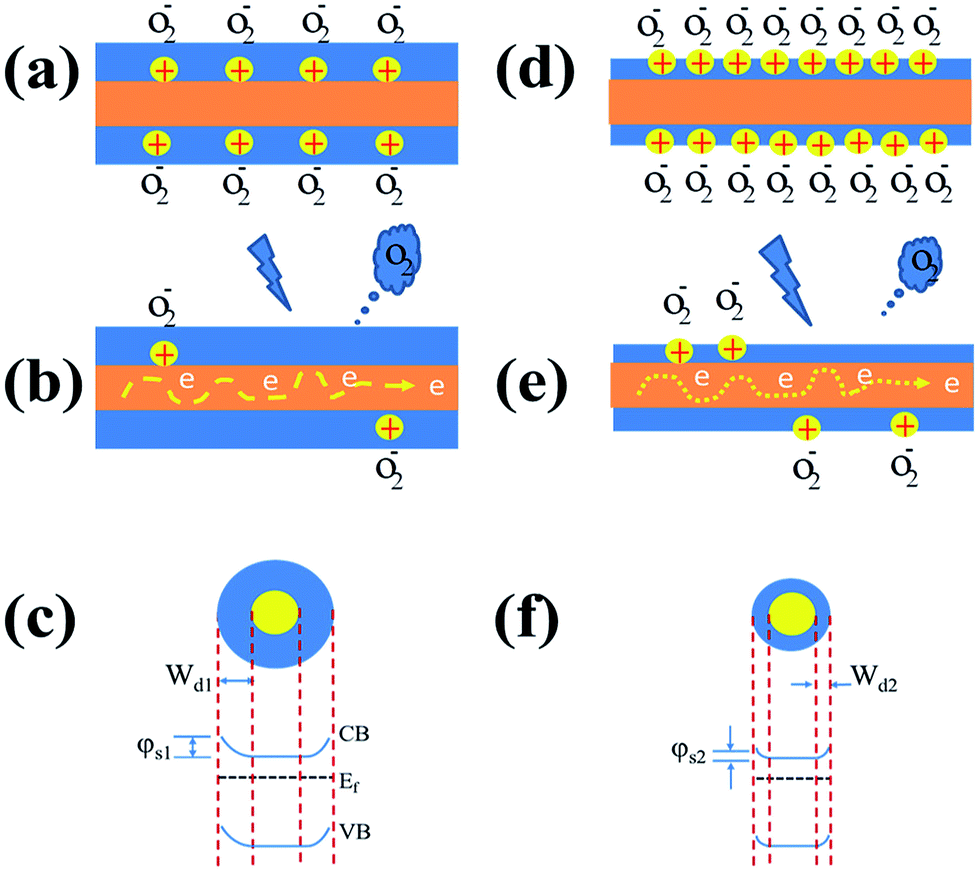 | ||
| Fig. 5 The adsorption/desorption of oxygen molecules mechanism of ZnO-NWs photoresponse (a–c) before and (d–f) after oxygen plasma treatment. The oxygen plasma treatment improves the oxygen vacancy-rich surface of ZnO NWs to enhance the electron depletion effect. CB and VB are the conduction and valence bands, respectively. | ||
Moreover, the free surface electrons of the nanowire channel are trapped due to the adsorption of oxygen molecules, which will result in the energy band structure with a relatively large surface depletion (Wd1) (Fig. 5a) and increased surface potential (φs1) (Fig. 5c). In contrast, the energy band structure observed after oxygen plasma treatment (Fig. 5f) showed a relatively small surface depletion width (Wd2) and reduced surface potential (φs2) due to the energetic ion bombardment (Fig. 5d) desorb from ZnO surface. This implied that the changes in charge density, surface depletion, and surface potential of the nanowire were affected by the surface modification with oxygen plasma treatment.
Conclusions
In summary, the modified properties of the ZnO NWs IDA-PDs before and after oxygen plasma treatment were investigated. Enhanced photocurrent and faster response speed were obtained because the surface contaminants on the ZnO NWs were eliminated by oxygen plasma treatment. The reason is that the surface depletion and surface potential of the nanowires could have been modulated by the surface modification secondary to the oxygen plasma treatment. This conclusion provides assistance in the further study of charge transport of the other photoelectrical materials and high-performance electronic devices.Conflicts of interest
There are no conflicts to declare.Acknowledgements
This work was supported by National Natural Science Foundation of China (Grant No. 51503207), Chongqing Research, Program of Basic Research and Frontier Technology (No. CSTC2017jcyjBX0030), the Scientific and Technological Project of Henan province (No. 182102210419)Notes and references
- S. Noda, A. Chutinan and M. Imada, Nature, 2000, 407(6804), 608 CrossRef PubMed.
- S. Noda, N. Yamamoto and M. Imada, et al., J. Lightwave Technol., 1999, 17(11), 1948–1955 CrossRef.
- Q. Chen, H. Ding and Y. Wu, et al., Nanoscale, 2013, 5(10), 4162–4165 RSC.
- M. C. Lin, C. J. Chu and L. C. Tsai, et al., Nano Lett., 2007, 7(12), 3656–3661 CrossRef.
- S. Song, W. K. Hong and S. S. Kwon, et al., Appl. Phys. Lett., 2008, 92(26), R829-4–43 Search PubMed.
- J. I. Sohn, Y. I. Jung and S. H. Baek, et al., Nanoscale, 2014, 6(4), 2046 RSC.
- W. K. Hong, G. Jo and J. I. Sohn, et al., ACS Nano, 2010, 4(2), 811–818 CrossRef PubMed.
- W. Li, L. Liao and X. Xiao, et al., Nano Res., 2014, 7(11), 1691–1698 CrossRef.
- K. Keem, J. Kang and C. Yoon, et al., Jpn. J. Appl. Phys., 2007, 46(9B), 6230–6232 CrossRef.
- S. Kim, H. Kim and D. B. Janes, et al., Nanotechnology, 2013, 24(30), 305201 CrossRef PubMed.
- C. Baratto, E. Comini and M. Ferroni, et al., CrystEngComm, 2013, 15(39), 7981–7986 RSC.
- D. M. Lee, J. K. Kim and J. Hao, et al., J. Alloys Compd., 2014, 583(3), 535–538 CrossRef.
- J. J. Dong, X. W. Zhang and J. B. You, et al., ACS Appl. Mater. Interfaces, 2010, 2(6), 1780–1784 CrossRef PubMed.
- Y. Li, M. Zhong and T. Tokizono, et al., Nanotechnology, 2011, 22(43), 435703 CrossRef PubMed.
- R. T. Khare and R. V. Gelamo, et al., Appl. Phys. Lett., 2015, 26(13), 31–178 Search PubMed.
- A. Y. Polyakov, N. B. Smirnov and A. V. Govorkov, et al., J. Appl. Phys., 2003, 94(6), 3960–3965 CrossRef.
- Q. Liu, M. Gong and B. Cook, et al., Phys. Status Solidi, 2017, 214(11), 1700176 CrossRef.
- J. Meena, M. C. Chu and Y. C. Chang, et al., J. Mater. Chem. C, 2013, 1(40), 6613–6622 RSC.
- A. G. Marrani, F. Caprioli and A. Boccia, et al., J. Solid State Electrochem., 2014, 18(2), 505–513 CrossRef.
- J. Lee, J. Chung and S. Lim, Phys. E, 2010, 42(8), 2143–2146 CrossRef.
- L. Guo, H. Zhang and D. Zhao, et al., Sens. Actuators, B, 2012, 166–167(10), 12–16 CrossRef.
- W. K. Hong, D. K. Hwang and I. K. Park, et al., Appl. Phys. Lett., 2007, 90(24), R829-3–21 CrossRef.
- W. K. Hong, G. Jo and S. S. Kwon, et al., IEEE Trans. Electron Devices, 2008, 55(11), 3020–3029 Search PubMed.
- J. J. Li, Z. Y. Gao and X. W. Xue, et al., Acta Phys. Sin., 2016, 65(11), 118104 Search PubMed.
- D. Ghosh, S. Kapri and S. Bhattacharyya, ACS Appl. Mater. Interfaces, 2016, 8(51), 35496–35504 CrossRef PubMed.
- N. Nasiri, R. Bo and L. Fu, et al., Nanoscale, 2017, 9(5), 2059 RSC.
- F. H. Alsultany, Z. Hassan and N. M. Ahmed, Opt. Mater., 2016, 60, 30–37 CrossRef.
- J. Lu, C. Xu and J. Dai, et al., Nanoscale, 2015, 7(8), 3396–3403 RSC.
- S. E. Ahn, J. S. Lee and H. Kim, et al., Appl. Phys. Lett., 2004, 84(24), 5022–5024 CrossRef.
- C. Soci, A. Zhang and B. Xiang, et al., Nano Lett., 2007, 7(4), 1003 CrossRef PubMed.
- M. Chen, L. Hu and J. Xu, et al., Small, 2011, 7(17), 2449–2453 Search PubMed.
- J. Dai, C. Xu and X. Xu, et al., ACS Appl. Mater. Interfaces, 2013, 5(19), 9344–9348 CrossRef PubMed.
- H. Li, J. Tao and J. Su, et al., Opt. Express, 2015, 23(16), 21204–21212 CrossRef PubMed.
- H. Kind, H. Yan and B. Messer, et al., Adv. Mater., 2010, 14(2), 158–160 CrossRef.
- J. Zhou, Y. Gu and Y. Hu, et al., Appl. Phys. Lett., 2009, 94(19), 191103 CrossRef PubMed.
- Y. Li, V. F. Della and M. Simonnet, et al., Nanotechnology, 2009, 20(4), 045501 CrossRef PubMed.
- K. Liu, M. Sakurai and M. Liao, et al., J. Phys. Chem. C, 2010, 114(114), 19835–19839 CrossRef.
- C. Soci, A. Zhang and X. Y. Bao, et al., J. Nanosci. Nanotechnol., 2010, 10(3), 1430–1449 CrossRef PubMed.
- Z. Zhan and L. Zheng, et al., Mater. Chem., 2012, 22, 2589–2595 RSC.
- A. S. Pawbake, K. K. Mishra and L. G. B. Machuno, et al., Diamond Relat. Mater., 2018, 84, 146–156 CrossRef.
- U. V. Patil, A. Pawbake and L. G. B. Machuno, et al., RSC Adv., 2016, 6(54), 48843–48850 RSC.
- T. C. Damen and S. P. S. Porto, et al., Phys. Rev., 1966, 142(2), 570–574 CrossRef.
| This journal is © The Royal Society of Chemistry 2018 |