
 Open Access Article
 This Open Access Article is licensed under a Creative Commons Attribution-Non Commercial 3.0 Unported Licence
Reversible and repeatable phase transition at a negative temperature regime for doped and co-doped spin coated mixed valence vanadium oxide thin films†
Dipta Mukherjeea,
Arjun Dey *b,
A. Carmel Mary Estherb,
N. Sridharab,
D. Raghavendra Kumarb,
A. Rajendrab,
Anand Kumar Sharmab and
Anoop Kumar Mukhopadhyay*a
*b,
A. Carmel Mary Estherb,
N. Sridharab,
D. Raghavendra Kumarb,
A. Rajendrab,
Anand Kumar Sharmab and
Anoop Kumar Mukhopadhyay*a
aAdvanced Mechanical and Materials Characterization Division, CSIR-Central Glass and Ceramic Research Institute, Kolkata-700 032, India. E-mail: mukhopadhyay.anoop@gmail.com; Tel: +91 33 2473 3469/76/77/96
bThermal Systems Group, U. R. Rao Satellite Centre (Formarly Known as ISRO Satellite Centre), Bangalore-560 017, India. E-mail: arjundey@isac.gov.in; arjun_dey@rediffmail.com; Fax: +91 80 2508 3203; Tel: +91 80 2508 3214
First published on 4th September 2018
Abstract
Smooth, uniform mixed valance vanadium oxide (VO) thin films are grown on flexible, transparent Kapton and opaque Al6061 substrates by the spin coating technique at a constant rpm of 3000. Various elements e.g., F, Ti, Mo and W are utilized for doping and co-doping of VO. All the spin coated films are heat treated in a vacuum. Other than the doping elements the existence of only V4+ and V5+ species is noticed in the present films. Transmittance as a function of wavelength and the optical band gap are also investigated for doped and co-doped VO thin films grown on a Kapton substrate. The highest transparency (∼75%) is observed for the Ti, Mo and F (i.e., Ti–Mo–FVO) co-doped VO system while the lowest transparency (∼35%) is observed for the F (i.e., FVO) doped VO system. Thus, the highest optical band gap is estimated as 2.73 eV for Ti–Mo–FVO and the lowest optical band gap (i.e., 2.59 eV) is found for the FVO system. The temperature dependent phase transition characteristics of doped and co-doped VO films on both Kapton and Al6061 are studied by the differential scanning calorimetry (DSC) technique. Reversible and repeatable phase transition is noticed in the range of −24 to −26.3 °C.
1. Introduction
Due to the zero extra energy requirement and large solar spectrum wavelength blocking effect, thermochromic materials have become the most cost effective smart window material. Owing to it's excellent thermochromic properties, vanadium dioxide (VO2) is the most explored thermochromic material for energy-saving smart window applications. Thus, above the phase transition temperature (Tt) VO2 exhibits a sharp first-order phase transition from the low temperature semiconducting monoclinic (P21/c) state to the high temperature metallic tetragonal rutile structure (P42/mnm) at around 68 °C.1–3 It can block infrared transmission (IR) above Tt and allow it below Tt. Some specific applications4–11 demand temperature regimes near zero or even sub-zero. These applications include smart window coating,4–6 IR switching and bolometric devices,7,8 CdTe detectors in passive radiant coolers and CdZnTe X-ray detectors in space astronomy payloads.9–11Hence, for an ideal thermochromic smart window material a sharp phase change at low temperature is required. The direct application of VO2 to smart windows is therefore restricted due to its high transition temperature of 68 °C. Reduction of Tt is thus of paramount importance for the applications of VO2 in passive smart radiator devices (PSRDs).12–15 PSRDs are the most economical solution for thermal control of micro/nano satellites and interplanetary missions where mass, volume and power are major constrains.12–15
Elemental doping has always been an efficient tool to tailor the Tt and optical properties of VO2 thin films.16 These aspects are achieved either by enhancing the carrier concentration or by inducing distortions in the crystal structure. As reported by Long et al.16 till date more than sixty elements have been investigated to dope in the VO2 lattice to tune the phase transition properties. According to Long et al.16 elemental doping with higher-valence elements like Mo and W aids to reduce the Tt by enhancing the carrier concentration of VO2. Also Sun et al.17 theoretically prove that doping with transition metals helps in reducing the Tt by lattice expansion of VO2. Among other dopants,18 F has been proved to be very efficient in reducing the Tt and also maintain a fairly good optical property by inducing structural distortion which leads to formation of defects in the VO2 lattice. Individual doping by F and W16 reduce (Tt) to 35° and 28 °C, respectively. However, co-doping19 with both W and F till date have caused the maximum reduction in Tt i.e., to about 0 °C.
On the other hand dopant like Ti20 fails to modulate the transition temperature but it can modify the colour of the VO2 based films efficiently by blue shifting the absorption edge at lower concentration of Ti doping. Several attempts21–25 are reported to reduce Tt of VO2 films to near room temperature or sub-zero temperatures. These films are obtained by sol–gel26,27 and sputtering28 etc. techniques. However, only a few19,29 have succeeded. For instance, Bukhardt et al.19 obtained the Tt of 0 °C for the (W and F) co-doped VO2 thin films. Recently, B doping has been utilized for significant reduction of Tt (e.g., 4 °C) in VO2 thin films.29
In view of the importance of nature and amount (i.e., at%) of doping, resulting phase structure recorded by XRD at room temperature, processing technique and the corresponding (Tt), a typical survey of literature data18–20,30–37 is presented in Table 1. A wide variety of processing techniques are employed. These include hydrothermal,18 RF sputtering,19 automatic coating,20,32,35 spin coating,30,37 melting–quenching-sol–gel method,31 dip coating,33,36 aerosol-assisted CVD34 etc. methods. It is interesting to note that a variety of dopants18,20,30–34 e.g., F, W, Mo, Zr, Ti, La, Nb and co-dopants e.g., Zr–W, Mg–W, F–W, Mo–F are utilized to reduce Tt. The amounts of single dopant range from 1.1 to 9.8 at%. These variations cause Tt to vary in the range from 28 to 68 °C. Further, almost all these researchers18,20,30–33 report the presence of the VO2 (M) phase recorded by XRD at room temperature. Unfortunately, phase analysis is not reported in some literature34 where single doping has been used.
| Dopants | Atomic percentages of doping (x%) | Technique/methods | VO2 (M) phase reported at room temperature | Transition temperature, Tt (°C) | References |
|---|---|---|---|---|---|
| F | 2.93 | Hydrothermal | ✓ | 35 | 18 |
| W | 2 | Spin coating | ✓ | 28 | 30 |
| Mo | 2 | Melting–quenching sol–gel method | ✓ | 41 | 31 |
| Zr | 9.8 | Films casted by automatic coating machine | ✓ | 64.3 | 32 |
| Ti | 1.1 | Films casted by automatic coating machine | ✓ | 68 | 20 |
| La | 4 | Dip coating | ✓ | 42 | 33 |
| Nb | 2.8 | Aerosol-assisted chemical vapour deposition | — | 41 | 34 |
| Zr + W | 8.5% Zr + 2.4% W | Films casted by automatic coating machine | ✓ | 28.6 | 35 |
| Mg + W | 4% Mg + 2% W | Dip coating | ✓ | 35 | 36 |
| F + W | 2.1% F + 1.8% W | RF sputtering | — | 0.14 | 19 |
| Mo + W | 1.02% Mo + 0.36% W | Spin coating | ✓ | 35 | 37 |
Further, the at% amounts of Zr–W, Mg–W, F–W, Mo–F co-dopants utilized by other researchers19,35–37 are 8.5% Zr + 2.4% W, 4% Mg + 2% W, 2.1% F + 1.8% W, 1.02% Mo + 0.36% W, respectively. These variations cause Tt to vary in the range from 0 to 35 °C. Moreover, almost all these researchers35–37 report the presence of the VO2 (M) phase recorded by XRD at room temperature. However, phase analysis is not reported in some literature19 where co-doping has been used.
Thus, as illustrated by the literature survey18–20,30–37 given in Table 1, the use of both doping and co-doping by Mo, W, Ti and F to reduce (Tt) of spin coated vanadium oxide thin films (VOTF) to as low as sub-zero temperature domain has not been significantly attempted before. This is what inspires us to take up this challenge. So, after these careful evaluations Mo, W, Ti and F have been selected as the doping and co-doping elements for efficient reduction in (Tt) with concomitant improvement in the optical transparency and colour modulation of mixed valence VOTF. It has been also suggested16 that increase in the amount of F may cause significant reduction in (Tt) but such an approach may compromise the optical properties of VOTF.
Therefore, three approaches are specifically taken in the present work. The first is ex situ incorporation of significant amount i.e., 30.08 at% F in the VOTF samples. The second is simultaneous introduction of (2.73 at% Mo + 30.08 at% F), (1.44 at% W + 30.08 at% F) and (5.33 at% Ti + 30.08 at% F) in the doped VOTF (i.e., DVOTF) samples. Finally, the third is the simultaneous introduction of (2.70 at% Ti + 1.34 at% Mo + 30.08 at% F) and (2.70 at% Ti + 0.70 at% W + 30.08 at% F) in the co-doped VOTF (i.e., CDVOTF) samples. The basic philosophy behind this approach is to check out if the (Tt) can be reduced to sub-zero temperatures without significantly compromising the optical properties of the thin films.
However, for successful application in the field of energy-efficient thermochromic smart window, optimization of luminous transmittance (Tlum) and solar modulation ability (ΔTsol) are also two additional key parameters to enhance performance.38,39 Although the luminous transmittance and solar modulating ability bears a mutual trade off relationship with Tt but this provides scope of further researches in this field to simultaneously improve the Tt as well as the optical properties. Also the problem of intrinsic yellow brown colour of the VO2 films and their low resistance towards aerial oxidation remain as major problems to be addressed.40 Although, an exact investigation into the aforesaid aspects is beyond the scope of the present work, their paramount importance deserves scope of our future work in this area. In a similar tune, the details of the complex issues related to simultaneous or non-simultaneous occurrences of structural and electronic phase transitions or even the absence of structural phase transition in the VOTF is kept in reserve as an objective of our future research endeavour.
Therefore, an attempt is made in the present work to decrease the (Tt) of spin coated VOTF to as low as sub-zero temperature domain for their potential PSRD applications towards the thermal control of spacecraft. Thus, the only major objective of the present work is to reduce (Tt) without significantly compromising the optical, especially the transmission properties of the VOTF, DVOTF and CDVOTF.
Accordingly, we have successfully deposited spin coated VOTF on both transparent, flexible Kapton and opaque Al6061 substrates by in situ doping of three transitional metals e.g., W, Mo and Ti along with ex situ doping of F in the vanadium oxide (VO) system. Thus, the DVOTF and CDVOTF are developed in the present work, as explained earlier. The DVOTF have Mo, W and Ti as the individual dopant in the respective cases. The CDVOTF have Ti–Mo, and Ti–W as the individual co-dopant in the respective cases. For both (DVOTF) and (CDVOTF) systems first the corresponding gels are prepared. Then they are spin coated from the corresponding gels.
The microstructural characterizations and phase analysis of the VOTF, DVOTF and CDVOTF are carried out by a variety of techniques. These include field emission scanning electron microscopy (FESEM), atomic force microscopy (AFM), X-ray diffraction (XRD) and X-ray photo electron spectroscopy (XPS) techniques. Further, the thermo-optical properties i.e., the average solar transmittance (τs), reflectance (ρs), absorptance (αs) and infrared (IR) emittance (εir) are evaluated for VOTF, DVOTF and CDVOTF. In addition, the sheet resistance (Rs) values are measured for all the thin films developed in the present work. Moreover, the reversible, repeatable smart phase transitions of VOTF, DVOTF and CDVOTF are confirmed by the differential scanning calorimetry (DSC) technique.
2. Experimental section
2.1 Substrate preparation
Kapton substrates of thickness ∼50 microns and Al6061 face-sheet of 0.5 mm thickness were used for the deposition of DVOTF and CDVOTF. Prior to casting of thin films the substrates were treated with 0.1 mL of 30% HF solution for five minutes. Since fluorine cannot be incorporated at higher temperatures into the VO system41 this technique of ex situ addition of fluorine was deliberately adopted as a process modification. These substrates were subsequently used for VOTF, DVOTF and CDVOTF depositions after the synthesis of the respective powders and gels as described below.2.2 Synthesis of powder and gel
Phase pure, heat-treated yellow coloured vanadium oxide powder was synthesized from ammonium metavanadate (NH4VO3, 99.0%, ACS reagent, Sigma Aldrich, Bengaluru, India) precursor. To synthesize VO gel, 1.3094 g of the synthesized vanadium oxide powder was dissolved in 80 mL of 15% H2O2 (Merck Specialties Pvt. Ltd., Mumbai, India). Hereafter, the prepared solution is termed as ‘solution A’ for the sake of brevity. Then, VO gel was prepared from the ‘solution A’. The detailed synthesis procedure of ‘solution A’ is described elsewhere.422.3 Thin film deposition
The resulting gel as described above in sub-section 2.2 was subsequently spin coated for 25 seconds at 3000 rpm as vanadium oxide thin film (VOTF) on the Kapton and Al6061 substrates prepared as mentioned above in sub-section 2.1. The Ti, Mo and W doped gels as mentioned in sub-section 2.2.1 above were subsequently spin coated for 25 seconds at 3000 rpm as doped vanadium oxide thin films (DVOTF) on the Kapton and Al6061 substrates prepared as mentioned above in sub-section 2.1. Similarly, the Ti–Mo and Ti–W co-doped gels as mentioned above in sub-section 2.2.2 were subsequently spin coated for 25 seconds at 3000 rpm as co-doped vanadium oxide thin films (CDVOTF) on the Kapton and Al6061 substrates prepared as mentioned above in sub-section 2.1. For all VOTF, DVOTF and CDVOTF depositions, a semi-automatic spin coater (Model No.: 121014, Delta Scientific Equipment Pvt. Ltd., Kolkata, India) was utilized.2.4 Post deposition heat treatment
All deposited VOTF, DVOTF and CDVOTF were subsequently heat treated for 1 h in a vacuum furnace (1.5 × 10⁻⁵ mbar, Hind High Vacuum, India). To have amorphous films the temperature of heat treatment was deliberately kept lower at 100 °C for all films deposited on the corresponding Kapton substrates. However, for all films deposited on the corresponding Al6061 substrates the temperature of heat treatment was raised to 450 °C while maintaining the same level of vacuum as maintained in the cases of the thin films deposited on the Kapton substrates. This process ensured development of crystalline films. In all heat treatments, the constant heating rates of 3 °C min−1 were maintained. The thickness of all the doped and co-doped thin films were measured to be around 340 nm since all the parameters (e.g., rpm and duration of deposition) were kept constant during the depositions of the VOTF, DVOTF and CDFVOTF.2.5 Final nomenclature of thin films
It may be recalled that all substrates were ex situ F doped prior to deposition of all the thin films. Hence, for ease of further discussions all VOTF are finally named as FVO. Similarly, Ti, Mo and W DVOTF are finally named as Ti–FVO, Mo–FVO and W–FVO, respectively. Further, both Ti–Mo and Ti–W CDVOTF are finally named as Ti–Mo–FVO and Ti–W–FVO, respectively.2.6 Phase analysis of thin films
The phase analysis of the vacuum heat treated FVO, Ti–FVO, Mo–FVO, W–FVO, Ti–Mo–FVO and Ti–W–FVO films grown on Kapton and Al6061 substrates were carried out by an X-ray diffractometer (X'pert Pro MPD, PANalytical, The Netherlands, Cu Kα1, λ ∼ 1.5414 Å, 40 kV, 35 mA, 5° ≤ 2q ≤ 80°). The 2θ step and data acquisition rates were kept constant at 0.05° min−1 and 0.5° min−1, respectively. The existing phases of the vacuum heat treated vanadium oxide thin films were indexed according to corresponding ICSD collection codes.Crystallite size (d) of the thin films grown on Kapton were evaluated by the well-known Scherrer's equation43 using (001) plane. This equation is given below.
 | (1) |
In eqn (1), d is crystallite size, K is a shape factor assumed to be 0.9, λ (=1.5414 Å) is the wavelength of the X-ray source as mentioned above, B is the full width at half maximum (FWHM) of the peak (001) and θ is the Bragg's angle.
2.7 Microstructural and surface topographical studies of thin films
The microstructural characterizations of the vacuum heat treated FVO, Ti–FVO, Mo–FVO, W–FVO, Ti–Mo–FVO and Ti–W–FVO films deposited on Kapton and Al6061 substrates were carried out by field emission scanning electron microscopy (FESEM, Supra VP35, Carl Zeiss, Germany). To avoid charging, prior to insertion in the FESEM chamber a thin (e.g., 50–70 Å) film of carbon was deposited on each of the samples. In addition, the surface topographies of these films were studied by using atomic force microscopy (AFM) technique in a conventional machine (Nanosurf easyScan 2, Switzerland).2.8 XPS study of thin films
The XPS studies of vacuum heat treated FVO, Ti–FVO, Mo–FVO, W–FVO, Ti–Mo–FVO and Ti–W–FVO films deposited on Kapton and Al6061 substrates were carried out using a SPECS (SPECS, Berlin, Germany) spectrometer. The spectrometer used an X-ray source of non-monochromatic Al Kα radiation (1486.6 eV) operated at 150 W (12 kV, 12.5 mA). The data were recorded with a single channel detector. The typical vacuum level maintained during the XPS experiments was about 5 × 10⁻⁵ mbar. The survey spectra were obtained with pass energy of 70 eV and step increment of 0.5 eV. Again, all the individual spectra were recorded with pass energy and step increment of 25 and 0.05 eV, respectively. The V 2p and O 1s components were curve-fitted with Gaussian–Lorentzian peaks after Shirley background subtraction employing the CasaXPS program. It needs to be noted that for indexing XRD peaks the ICSD collection codes from the standard data base were used. However, in the case of indexing XPS peaks only the values of binding energies are available in reported literature for detection of elemental oxidation states. The XPS peaks reported in the present study matched well with our earlier reported values42,44,45 as well as those reported in literature.46–492.9 Thermo-optical and electrical characterizations of thin films
The average solar transmittance, reflectance and absorptance of the vacuum heat treated FVO, Ti–FVO, Mo–FVO, W–FVO, Ti–Mo–FVO and Ti–W–FVO films deposited on Kapton and Al6061 substrates were evaluated both in reflectance and transmittance modes as per ASTM C1549-09. For this purpose, a solar spectrum reflectometer (SSR-E, Devices and Services Co., USA) was used. The average IR emittance of the deposited films was measured following the ASTM standard C1371-04a. These data were recorded in an emissometer (AE, Devices and Services Co., USA). The transmittance spectra of films were recorded as a function of wavelength in the solar region (200 nm to 2300 nm) of the spectral window. For this purpose, an UV-VIS-NIR spectrophotometer (Cary 5000, Agilent Technologies, USA) was utilized. Further, the sheet resistance (Rs) values of the spin coated films deposited on Kapton were measured using a four-point probe (Jandal 3000 Instrument, USA).2.10 Studies of phase transition of thin films
The phase transition temperatures of the vacuum heat treated FVO, Ti–FVO, Mo–FVO, W–FVO, Ti–Mo–FVO and Ti–W–FVO films deposited on Kapton and Al6061 substrates were determined by the DSC technique using a conventional machine (Q100, TA Instruments, USA). All the DSC experiments were conducted in helium environment. Also, in all the DSC experiments both heating and cooling rates were kept constant at 10 °C min−1.3. Results and discussion
3.1 XRD analysis
Fig. 1a and b represent the XRD patterns of the vacuum heat treated FVO, Ti–FVO, Mo–FVO, W–FVO, Ti–Mo–FVO and Ti–W–FVO films deposited on Kapton and Al6061 substrates, respectively. In both the cases the peaks are thoroughly indexed as per the corresponding ICSD collection codes. The FVO, Ti–FVO, Mo–FVO, W–FVO, Ti–Mo–FVO films deposited on Kapton show the presence of maximum intensity peak along the direction of (001) plane at about 2θ of 8°. These data confirm the presence of V2O5·nH2O system (ICSD collection code-94905). The presence of monoclinic VO2 phases (ICSD collection code-73855, space group C12/M1) are identified at 2θ of 33° and 42°. On the other hand, the peaks between 2θ of 10° to 30° appear from the corresponding Kapton substrates.50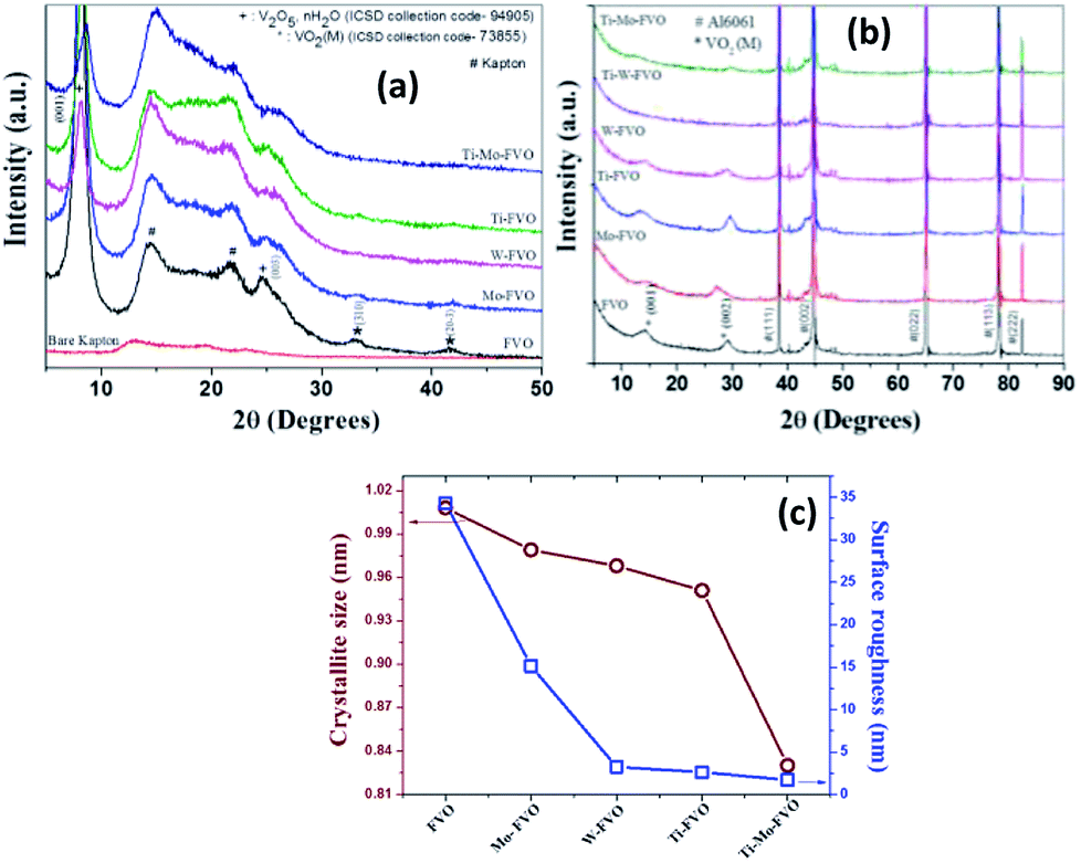 | ||
| Fig. 1 XRD pattern of the vacuum heat treated FVO, Ti–FVO, Mo–FVO, W–FVO, Ti–Mo–FVO and Ti–W–FVO films deposited on (a) Kapton and (b) Al6061 substrates; (c) crystallite size and root mean square (RMS) surface roughness of the films deposited on Kapton substrates. | ||
Similarly, in the cases of the FVO, Ti–FVO, Mo–FVO, W–FVO, Ti–Mo–FVO and Ti–W–FVO films deposited on Al6061, the peaks at 2θ of 14.3° and 29.26° are due to the respective presence of the (001) and (002) planes of monoclinic VO2 phase (ICSD collection code-73855, space group C12/M1). On the other hand, the peaks at 2θ of 38.24°, 44.35°, 65°, 78° and 82.41° emerge from the corresponding Al6061 (ICSD collection code-53773) substrates. It is interesting to note that both the crystallite size (d) and the RMS surface roughness values of the vacuum heat treated FVO, Ti–FVO, Mo–FVO, W–FVO, Ti–Mo–FVO and Ti–W–FVO films decrease with increase in the number of doping elements (Fig. 1c).
3.2 FESEM, EDX and AFM studies
Fig. S1(a–e) and S2(a–e)† show respectively the typical FESEM micrographs and corresponding EDX data of the vacuum heat treated FVO, Ti–FVO, Mo–FVO, W–FVO, Ti–Mo–FVO and Ti–W–FVO films deposited on Kapton substrates. Similarly, Fig. S3(a–f)† represent typical FESEM micrographs of the vacuum heat treated FVO, Ti–FVO, Mo–FVO, W–FVO, Ti–Mo–FVO and Ti–W–FVO films deposited on Al6061 substrates. The signatures of pertinent doping elements are clearly observed in corresponding EDX spectra but not shown here, for the sake of brevity. All films but FVO deposited on the Kapton substrates show uniform, smooth and dense surface microstructures. The FVO films on Kapton and all films deposited on the Al6061 substrates show granular surface microstructures. The AFM surface topographies, Fig. S4(a),† of the FVO films on Kapton substrate confirm the granular features. On the other hand, the AFM surface topographies of Ti–FVO, Mo–FVO, W–FVO, Ti–Mo–FVO and Ti–W–FVO films deposited on Kapton substrates confirm the uniform, smooth and dense surface features.3.3 XPS studies
Typical illustrative V 2p and O 1s core level spectra of the vacuum heat treated FVO, Ti–FVO, Mo–FVO, W–FVO, Ti–Mo–FVO and Ti–W–FVO films deposited on the Kapton and Al6061 substrates are shown in Fig. 2(a–e) and 3(a–f), respectively. Binding energies of vanadium species as obtained from V 2p core level spectra along with the relative peak intensities of all the films deposited on the Kapton substrates are summarized in Table S1.† Similar data of all the films deposited on the Al6061 substrates are summarized in Table S2.† These data confirm the presence of only V5+ and V4+ species in all the films. Further, the typical curve fitted core level spectra in Fig. 4(a–c) confirm the respective presences of Mo 3d, W 4f and Ti 2p in the thin films deposited on the Al6061 substrates. Similarly, the typical curve fitted core level spectra in Fig. 4(d–e) confirm the respective presences of Mo 3d and Ti 2p in the thin films deposited on the Kapton substrates.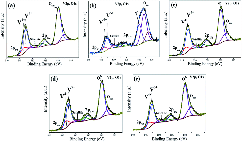 | ||
| Fig. 2 Curve-fitted V 2p and O 1s core level spectra of the vacuum heat treated (a) FVO, (b) Ti–FVO, (c) Mo–FVO, (d) W–FVO, (e) Ti–Mo–FVO films deposited on Kapton substrates. | ||
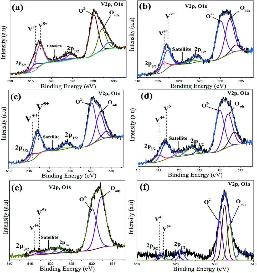 | ||
| Fig. 3 Curve-fitted V 2p and O 1s core level spectra of (a) FVO, (b) Mo–FVO, (c) W–FVO, (d) Ti–FVO, (e) Ti–W–FVO and (f) Ti–Mo–FVO thin films on Al6061 substrates. | ||
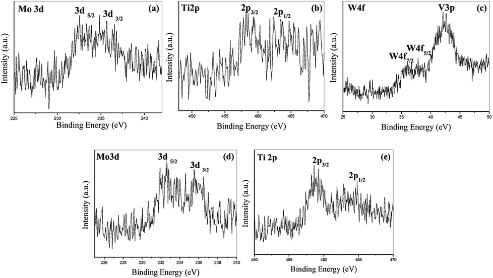 | ||
| Fig. 4 Typical curve-fitted core level spectra of (a) Mo 3d, (b) Ti 2p, (c) W 4f orbitals in the thin films deposited on the Al6061 substrates and typical curve-fitted core level spectra of (d) Mo 3d, (e) Ti 2p orbitals in the thin films on the Kapton substrates. | ||
3.4 Evaluation of sheet resistance
The Rs values of the vacuum heat treated FVO, Ti–FVO, Mo–FVO, W–FVO, Ti–Mo–FVO and Ti–W–FVO films deposited on Kapton substrates are shown in Fig. 5. The highest resistance value is measured for FVO system and the resistance decreases further as follows: FVO > Mo–FVO > W–FVO > Ti–FVO > Ti–Mo–FVO. Increase in number of doping elements lead to enhancement of carrier density and oxygen vacancies. These factors may contribute to the decrease in the Rs values following the order as mentioned above.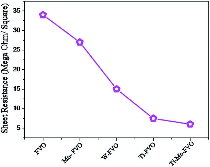 | ||
| Fig. 5 Sheet resistance values of doped and co-doped VO thin films on Kapton substrate. | ||
3.5 Study of thermo-optical properties
The average absorptance, reflectance and transmittance of the various thin films deposited on the Kapton substrates are shown in Fig. 6(a–c). Highest αs is obtained for FVO system and further it decreases in the order as FVO > Mo–FVO > W–FVO > Ti–FVO > Ti–Mo–FVO. However, the opposite trend is observed for ρs and τs. The εir values of the various thin films are almost unaltered as compared to that of the εir of bare Kapton (Fig. 6d). This observation also supports the IR transparency behaviour of the present vanadium oxide thin films. The data plotted in Fig. 6e represent the effect of doping on αs and ρs of the various thin films deposited on the optically opaque Al6061 substrates. The αs for the VO thin films on Al6061 show almost decreasing trend from FVO to Ti–Mo–FVO while ρs offer an ascending order from FVO to Ti–Mo–FVO. It is very interesting to note that upon co-doping, the average αs is effectively reduced to 0.7 for Ti–Mo–FVO thin films from a value of around 0.8 for FVO thin films deposited on the Al6061 substrate.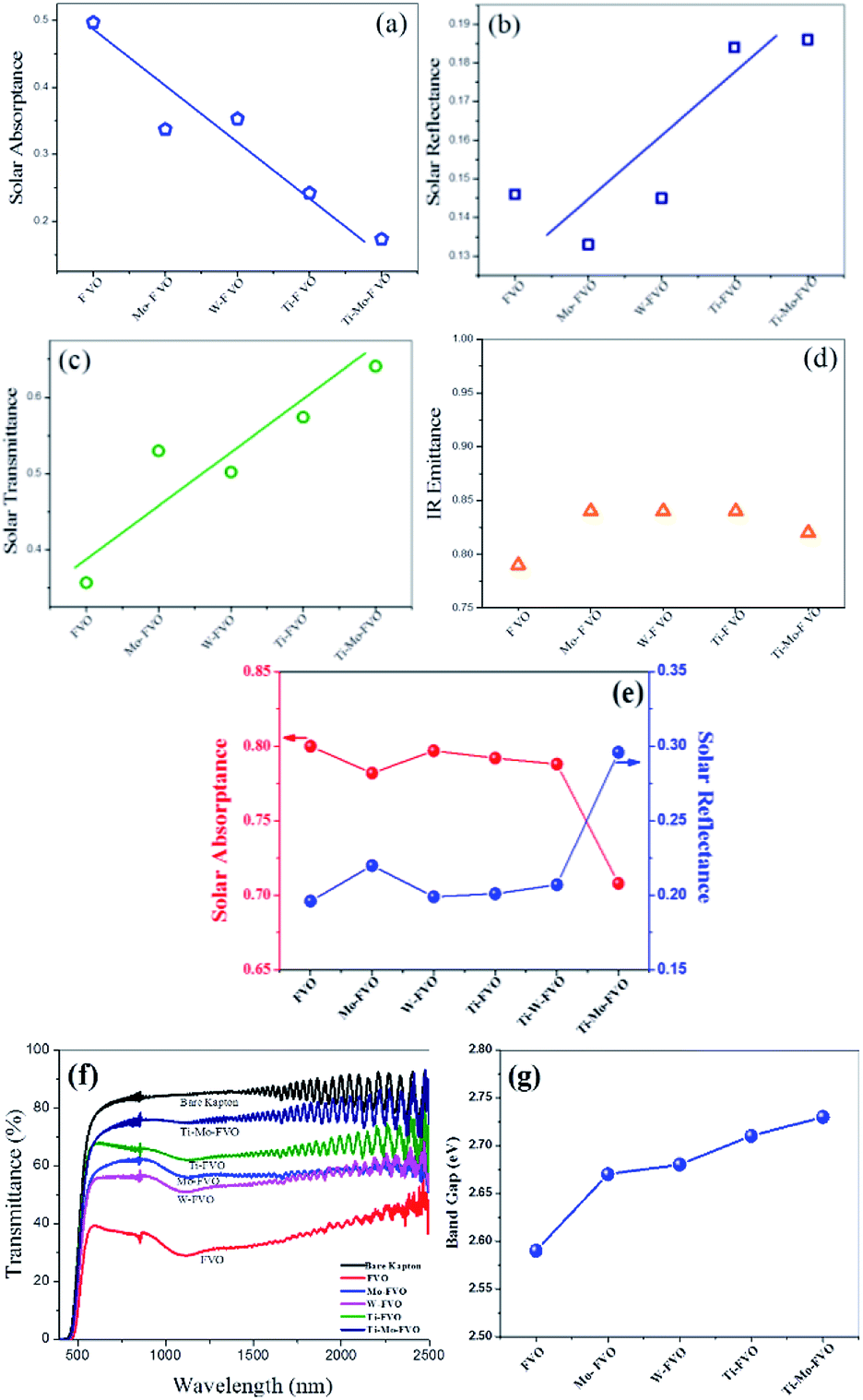 | ||
| Fig. 6 Variation of solar (a) absorptance, (b) reflectance, (c) transmittance and (d) IR emittance of the thin films deposited on the Kapton substrates. (e) Effect of doping on solar absorptance and solar reflectance of the thin films deposited on the Al6061 substrates. (f) Transmittance of the thin films deposited on the Kapton substrates as a function of wavelength. (g) Optical band gaps of the thin films deposited on the Kapton substrates. | ||
Further, for all the films grown on the Kapton substrates the variations of τs as a function of wavelength are shown in Fig. 6f. It is evident from the data plotted in Fig. 6f that in visible and near IR regions, the Ti–Mo–FVO thin films exhibit the highest (i.e., around 75%) transmittance while the FVO thin films exhibit the lowest (i.e., around 35%) transmittance. It needs to be noted that the surface roughness was the highest for the FVO thin films and the lowest for the Ti–Mo–FVO thin films (Fig. 1c). Therefore, it is plausible to argue that the decrease in transmittance (Fig. 6f) is linked with the increase in the corresponding surface roughness (Fig. 1c) of the thin films. Similar observations are also reported by others.45,51,52
Actually, the transition elements like Ti, Mo and W plays the role of electron donor to the 3d band of vanadium.19 Donation of electrons by these transition elements to V 3d band along with the presence of fluorine stabilizes the metallic phase, which in turn enhances the transmittance properties of the corresponding co-doped thin films.
Fig. S5(a–e)† represent the plots of (αhυ)2 versus photon energy of the vacuum heat treated FVO, Ti–FVO, Mo–FVO, W–FVO, Ti–Mo–FVO films deposited on the Kapton substrates. Optical band gap (Eg) values for the thin films are evaluated using the well-established Tauc's equation. These data are plotted in Fig. 6g. Among the samples, the Ti–Mo–FVO thin films exhibit the highest Eg value of 2.73 eV while the FVO thin films exhibit the lowest Eg value of 2.59 eV. The enhancement in Eg value indicates the shift of the primary absorption edge towards the shorter wavelengths. The transmittance behaviours (Fig. 6f) of the thin films deposited on the Kapton substrates also support the present trend of variations (Fig. 6g) in Eg.
3.6 Study of phase transition temperature
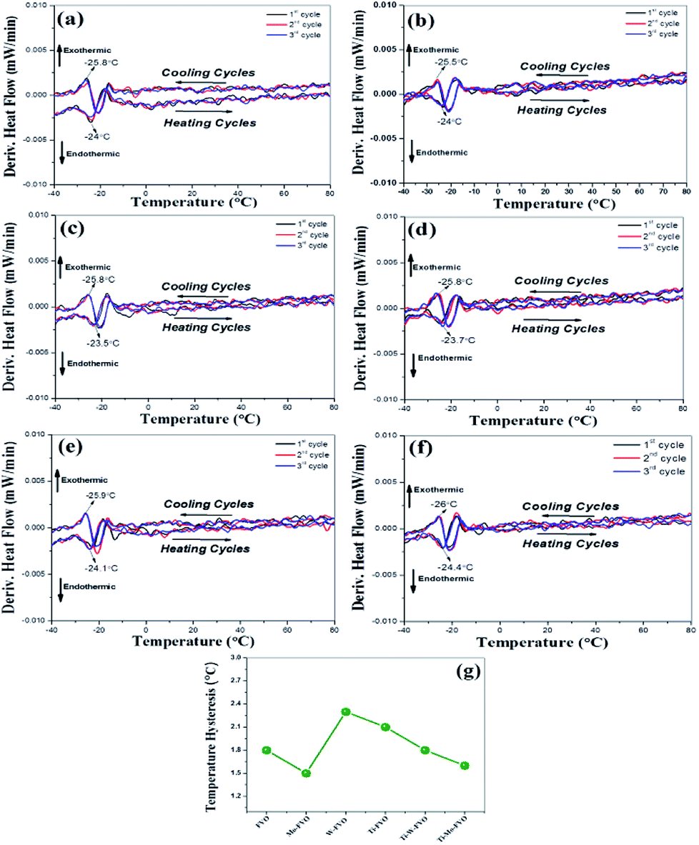
For all the thin films deposited on the Kapton and Al6061 substrates, the DSC curves and transition temperature hysteresis plots are presented in Fig. 7(a–f) and 8(a–g), respectively. These data establish beyond any doubt the reversible and repeatable signature of smart phase transition temperature (Tt) range of −24 to −26.3 °C for all the VO thin films deposited on both the substrates. Thus, the present result is the first ever report where F doping and other transition element co-doping gives a reversible as well as repeatable smart, phase transition at sub-zero temperatures in VO thin films. This claim is amply supported by the fact that (Tt) around only 0 °C is reported for VO thin films with and without W–F and B doping and/or co-doping.19,29 The transition temperature hysteresis plots exhibit the difference between the transition temperatures observed during the heating and corresponding cooling cycles. These data are plotted in Fig. 7f for the FVO, Mo–FVO, W–FVO, Ti–FVO and Ti–Mo–FVO thin films deposited on the Kapton substrates. Similar data are plotted in Fig. 8g for the FVO, Mo–FVO, W–FVO, Ti–FVO, Ti–Mo–FVO and Ti–W–FVO thin films deposited on the Al6061 substrates. These data confirm that the temperature hysteresis is in the range of 1.5 to 2.3 °C. Thus, the present data confirms the repeatability of the smart phase transition temperature (Tt) of the VO thin films developed in the present work. | ||
| Fig. 7 DSC curves of (a) FVO, (b) Mo–FVO, (c) W–FVO, (d) Ti–FVO and (e) Ti–Mo–FVO and (f) transition temperature hysteresis; of all the thin films deposited on the Kapton substrates. | ||
 | ||
| Fig. 8 DSC curves of (a) FVO, (b) Mo–FVO, (c) W–FVO, (d) Ti–FVO, (e) Ti–W–FVO, (f) Ti–Mo–FVO and (g) transition temperature hysteresis of all the thin films deposited on the Al6061 substrates. | ||
3.7 Structure–property correlations
It needs to be noted that in the present work the amorphous natures of the 100 °C vacuum heat treated VOTF, DVOTF and CDVOTF (Fig. 1a) deposited on the Kapton substrates do not hamper the phase transition properties (Fig. 7) of these thin films. Similar observation is also reported by Porwal et al.44 In this case44 also, the amorphous RF sputtered VO thin films exhibit reversible, repeatable (Tt) in the range of 337–343 °C. Therefore, in view of results reported already in literature44 and those obtained in the present work; it seems plausible to argue that amorphous VO thin films can and very well do exhibit reversible, repeatable (Tt). However, the magnitude of (Tt) can be a sensitive function of the processing techniques which in turn govern the microstructures of the resulting thin films. In addition, the major factor that determines the reversible, repeatable (Tt) is the relative abundance or absence of the V4+ species in the surface of the VO thin films. Thus, in the current work the sole motto of vacuum heat treatment was to generate V4+ by dissociation of V2O5, which, in turn; helps to reduce the phase transition temperature (Fig. 7). Moreover, it is already reported by Porwal et al.44,45 that vacuum heat treatment at lower temperature (i.e., 100 °C) has not only generated V4+ but also improved the optical transmittance in the NIR region. In addition, it also aids in reducing both the (Tt) and the sheet resistance. The data obtained in the current work are similar to those reported by Porwal et al.44,45 and hence, should be accepted as facts.The sheet resistance values showed a decreasing trend with increase in the number of dopants. However, the difference is not spectacular e.g., from mega ohm to ohm range. All the Rs values are in mega ohm range. The difference between the highest and lowest values of Rs is only 25 mega ohm. As mentioned already, this happens due to the presence of more number of doping elements that increase the carrier concentration. The enhanced carrier concentration, in turn, lowers the sheet resistance value. Also, the same can be proved from DSC measurements (Fig. 7 and 8) where the Ti–Mo–FVO thin films have shown the maximum decrement in (Tt) due to enhanced carrier concentration. The sheet resistance also is the lowest for the Ti–Mo–FVO thin films.
Now regarding the concentration of dopants, the F concentration is kept intentionally higher than other dopants (viz. Ti, Mo, and W) since it is evident from literature16,19 that enhancement of F doping percentage results in higher reduction of (Tt). On the other hand besides F, the other doping elements (viz. Ti, Mo and W) are actually used in the current study to tune the optical properties by varying their doping levels while keeping the reduction of (Tt) intact. Hence, the atomic percentage of fluorine (F) in FVO thin films has been kept constant at 30.08 at%. In the Mo–FVO thin films the concentration of F is constant at 30.08 at% but Mo is present in 2.73 at%. Similarly in W–FVO thin films the concentration of W and F are 1.44 at% and 30.08 at%, respectively. Also in Ti–FVO thin films the concentration of Ti and F are 5.33 at% and 30.08 at%, respectively. Finally in Ti–Mo–FVO thin films the concentration of Ti, Mo and F are kept at 2.70 at%, 1.34 at% and 30.08 at% respectively. Similarly in Ti–W–FVO thin films the concentration of Ti, Mo and F are kept at 2.70 at%, 0.70 at% and 30.08 at% respectively. Further, all the sheet resistance values reported in this study are in mega ohm range. Thus, the minor differences in their absolute magnitudes are attributed mainly to the different carrier concentrations.
3.8 Issues related to phase transition
There is an apparent contradiction between the observation of absence of the metallic phase VO2 (R) in the XRD spectra recorded at room temperature (Fig. 1a and b) and the observation of reversible, repeatable phase transition temperatures (e.g., −24° to −26 °C, Fig. 7 and 8) in the DSC data. The important phenomenon of semiconductor to metal phase transition was first discovered and extensively elaborated by N. F. Mott in 1949.53According to Mott, the primary cause of the transition is the genesis of electrons and corresponding holes within the lattice depending upon which the material behaves either as metal or semiconductor. But, it is also mentioned53 that sometimes the atoms from which the electrons are missing, couple with another atom to exist as ion pairs in the same lattice and ultimately becomes a semiconductor from conductor.
Similar kind of observations are reported by Bukhardt et al.19 where it is stated that the presence of W and F in the vanadium oxide lattice destroys the V4+ – V4+ ion pairs and thus, destabilizes the semiconducting phase. This destabilization, in turn, leads to decrease in the transition temperature.
But these authors19 also mention that in presence of other dopants, F improves the visible transmittance as well as enhances the band gap energy by blue shifting the absorption maxima to lower edges. In the present study, reversible, repeatable (Tt) in the range of −24 to −26.3 °C (Fig. 7 and 8) is achieved due to the presence of V4+ along with other doping elements. This happens despite the fact that V5+ is present in relatively larger content in the films (Tables S1 and S2†). Therefore, the XRD data recorded at room temperature show the monoclinic VO2 phase along with V2O5·nH2O. This is probably because of the ion pair formation as suggested by N. F. Mott.53
Similar kind of suggestions are also reported by Tang et al.54 where homopolar V4+ – V4+ bond formation stabilizes the semiconducting phase of vanadium oxide, which, in turn stabilizes the monoclinic phase of VO2. Moreover, in the present study all the films are either doped or co-doped in nature. Now what does the doping do? It basically enhances the carrier density55 of ions, which, in turn lowers the energy barrier to make the structural as well as electronic phase transition happen at lower ranges of temperatures.
However, these results should be further discussed in terms of a very recent, interesting viewpoint put forward by Banerjee et al.55 They opine55 that the phase transition in VO2 is an independent phenomenon which can happen even without a structural phase transition. This is exactly what is also reflected from the experimentally measured data of the present work. It is also suggested55 that a metallic phase can be induced even without the conventionally expected structural phase change if thermal excitation of the carriers approaches a threshold density. These researchers55 have taken resort to several experimental data as well as literature56−58 data to contradict the conventional wisdom about the simultaneous occurrences of structural and electronic phase transitions in VO2. Instead, they have suggested55 VO2 to be a poor metal with relatively low mobility values (1–10 cm2 V−1 s−1). It has been concluded further55 that the phase transition uniquely depends only on the density of the charge carriers regardless of their origin. Similar is the case of the present study too, where; in spite of observing phase transition at lower region of temperature; a signature of tetragonal/rutile phase is not recorded at room temperature.
On the other hand, Bukhardt et al.19 has also stated that when F alone is doped in the vanadium oxide lattice, the semiconducting phase gets stabilized whereas in presence of other dopants along with F the metallic character gets enhanced. A similar situation prevails in the present study. Here, the sheet resistance decreases in the order FVO > Mo–FVO > W–FVO > Ti–FVO > Ti–Mo–FVO. This happens despite the fact that the sheet resistance values are in the mega ohm range. These higher resistance values are expected because, compared to the minor V4+ species; the V5+ species is the major contributing species.
In this connection, it may be recalled that RF sputtered VOTF44 on Si give sheet resistance (Rs) of 105–106 Ω per square. However, RF sputtered VOTF45 on quartz give sheet resistance (Rs) of 4.43 × 10⁶–71 × 106 Ω per square. On the other hand, vacuum heat treated spin coated VOTF42 on quartz give sheet resistance (Rs) of 104–106 Ω per square and (Tt) of 44–48 °C. Again, a recent report59 show that RF-plasma-assisted oxide MBE deposited VO2 thin films on TiO2 have sheet resistance (Rs) of 103–106 Ω per square and (Tt) of 60 °C. Thus, the (Rs) data obtained in the present work match nicely with those reported in literature42,44,45,59 although the compositions are different. Further, these (Rs) values could be achieved along with a significant reduction of (Tt) to −24° to −26 °C which could be achieved by appropriate tuning of the amounts and nature of dopants and co-dopants in the present work.
Moreover, at room temperature V2O5 is semiconducting and VO2 is also poorly conducting as suggested by Banerjee et al.55 This fact55 thus corroborate well with the sheet resistance results obtained in the current study. Another important achievement of the present study is the improvement in the visible transmittance property which again might be attributed to the incorporation of doping elements. Similar logic has been suggested by Bukhardt et al.19
There is another important aspect that needs to be understood as well. Actually, phase transformation is very sharp and fast phenomenon in VO2 system.60 Therefore, it appears plausible to argue that such a fast process cannot be necessarily always possible to be correctly and adequately monitored by the conventional XRD technique. The logic behind this supposition is the possibility55 that the structural phase transition may not always occur simultaneously with the electronic phase transition.
Hence, the more sensitive DSC measurements appear to be a more appropriate choice that was dedicated in the present work to capture the phase transition properties. Also in a recent report by Fang et al.61 it has been confirmed that doping metal ions in the VO2 lattice not only causes reduction in phase transition temperature but also improves the transmittance property depending upon the at% percentages of dopants. Upon 3 at% of W doping, this work61 reports the significant reduction of the transition temperature to the lowest magnitude of 10.6 °C.
These authors61 also note that doping causes many structural deformations of the moiety including broadening as well as huge shifting of the XRD peaks. In the case of undoped VO2 samples, XRD spectra recorded at room temperature confirmed the formation of the VO2 (M) monoclinic phase at a 2θ value of 25.34° after vacuum heat treatment at 450 and 500 °C. However, for 3 at% W doped VO2 samples XRD spectra recorded at room temperature confirmed62 the formation of the VO2 (M) monoclinic phase at a 2θ value of (20°) that is much lower than that (25.34°) noted in the case of the undoped VO2 samples. Therefore, it appears plausible to argue that there is actually no contradiction between the observation of absence of the metallic phase VO2 (R) in the XRD spectra recorded at room temperature and the observation of reversible, repeatable phase transition temperatures (e.g., −24° to −26 °C, Fig. 7 and 8) in the DSC data.
Nevertheless, there cannot be any doubt that for VOTF, DVOTF and CDVOTF the complexities related to presence or absence of structural phase transition and its effect on phase transition temperature is yet to be fully understood.19,55–59 Similarly important is to further our understanding about the simultaneous or non-simultaneous occurrences of the structural and electronic phase transitions55 and their roles in reducing or enhancing the phase transition temperatures of VOTF, DVOTF and CDVOTF.
In this context it is important to note that there is a sizeable amount of evidence and related viewpoints which rather strongly suggest that actually the phase transition originate from overlapping interactions of several important physical processes.59 These include electronic correlation and interactions. These interactions typically involve spin, lattice, and charge degrees of freedom. It is further shown59 that in VOTF spatially separated regions can coexist. These regions possess distinct structural properties. They also possess distinctly different magnetic as well as electronic properties.
In a more generalized way of physically conceptualizing the scenario it can be described as a multi-scale phase separation. However, here the phase separation occurs between two (or more) phases. The most important point to note is that these phases have magnitudes of free energy which are comparable to each other.59 It has been shown59 that such heterogeneity can span over wide length scales of the corresponding microstructure. If this picture is correct, then, such heterogeneity may eventually span from as small as the local atomic scale domain to the mesoscale domain.59
Therefore, it seems plausible to argue that if such networks of multiple domains exist in VOTF, they will play major roles in the detailed dynamics of phase transition processes, which, themselves are yet to be unambiguously understood. Nevertheless, these dynamics will ultimately control both structural and electronic aspects of the phase transition behaviour.19,55,59
Recent work62 conducted using the temperature-dependent synchrotron radiation and Raman spectroscopy on 13 nm thick strained VO2 films deposited on TiO2 provide strong evidence that the structural phase transition in the temperature range near the MIT gets suppressed by the presence of epitaxial strain. It is also proved62 that the very presence of the same epitaxial strain initiates the electronic transition that leads to the MIT.
In addition to these viewpoints another slightly different but conforming viewpoint63 also seems to be emerging. This viewpoint is also concerned with presence of interfacial strain in VOTF. It has been very recently63 suggested that the interfacial strain strongly affects the electronic orbital occupancy. The localized variation in the electronic orbital occupancy changes also the electron–electron correlation. The change in the electron–electron correlation,63 in turn, controls the phase transition temperature.63
Thus the detailed interconnections between nature and magnitude of epitaxial strain, electron orbital occupancy, relative ease or difficulty of simultaneous and/or non-simultaneous occurrences of structural and electronic phase transitions and the magnitude of (Tt) in VOTF needs to be studied in a dedicated manner. Although the same is beyond the scope of the present work, its importance should be deeply appreciated. The reason is simply that it can open up a new paradigm of generating the ability to tune the phase transition in VOTF through intelligent exploitation of the interfacial strain engineering. Hence, such an attempt should definitely frame the scope of future work in this area.
3.9 Importance of doped and co-doped vanadium oxide films for space application
Considering the smart radiation device applications for spacecraft thermal control, the usage of present DVOTF and CDVOTF could be prospective. In particular, this film would be potential candidates for the passive cooling purpose of CdTe and CdZnTe X-ray detectors for astronomically relevant payloads where the detector would be operational only in the sub-zero temperature regime (e.g., in the range of −20 to −30 °C).10,11 The present work also highlights the capability to tune from low to high optical transparency property by suitable co-doping without significant alteration of (Tt).On the basis of the lowest absorptance (Fig. 6a and e) and the highest transmittance (Fig. 6c and f) the Ti–Mo–FVO thin film is likely to be the best option from the point of view of smart radiative thermal control application in satellites. However, it should be also possible to pick up any of the appropriate systems offered in the present developmental work with the desired optical properties and then the same may be usable to achieve effective passive thermal control.
4. Conclusions
Vanadium oxide thin films are grown on flexible, transparent Kapton and opaque Al6061 substrate by sol–gel spin coating technique at 3000 rpm. Incorporations of doping elements like – Ti, Mo, W and F are successfully done at particular at% in VOTF systems. The VOTF exhibit remarkable reductions in the phase transition temperature, Tt (i.e., −26.3 °C) accompanied by a significant enhancement (∼75%) in visible/NIR transmittance properties for the first time. The incorporation of F in VOTF system accounts for a considerable reduction in Tt (i.e., −24 °C) with trade off in transmittance (∼35%). Further, CDVOTF Ti–Mo–FVO shows the highest optical transparency (∼75%) and lowest Tt (i.e., −26.3 °C). Thus, generally the present films could be used efficiently in passive smart radiative device applications for spacecraft thermal control and particularly as coating for passive radiant cooler components for CdTe or CdZnTe X-ray detectors of space astronomy payloads.Conflicts of interest
The authors of this present study do not have any conflict of interest to declare.Acknowledgements
Two of the authors (D. M. and A. K. M.) appreciate the kind supports and encouragements received from Dr K. Muraleedharan, Director, CSIR-CGCRI, Kolkata during the course of the present work. These authors also acknowledge the supports received from AMMCD of CSIR-CGCRI. The financial support of the Indian Space Research Organisation (ISRO) through the RESPOND Project (No. GAP 0245) is gratefully acknowledged. Further, the authors are grateful to Dr Harish C. Barshilia, Dr Parthasarathi Bera, Ms. Latha and Mr Srinivas of CSIR-NAL for facilitating XPS and UV-VIS-NIR experiments, under ISRO rate contract.References
- D. Natelson, Nature, 2013, 500, 408, DOI:10.1038/500408a.
- Z. Zhang, Y. Gao, Z. Chen, J. Du, C. Cao, L. Kang and H. Luo, Langmuir, 2010, 26, 10738–10744, DOI:10.1021/la100515k.
- N. Wang, M. Duchamp, R. E. Dunin-Borkowski, S. Liu, X. Zeng, X. Cao and Y. Long, Langmuir, 2016, 32, 759–764, DOI:10.1021/acs.langmuir.5b04212.
- S. Wang, K. A. Owusu, L. Mai, Y. Ke, Y. Zhou, P. Hu, S. Magdassi and Y. Long, Appl. Energy, 2018, 211, 200–217, DOI:10.1016/j.apenergy.2017.11.039.
- Y.-S. Yang, Y. Zhou, F. B. Y. Chiang and Y. Long, RSC Adv., 2017, 7, 7758–7762, 10.1039/C6RA24686A.
- Q. Hao, W. Li, H. Xu, J. Wang, Y. Yin, H. Wang, L. Ma, F. Ma, X. Jiang and O. G. Schmidt, Adv. Mater., 2018, 30, 1705421, DOI:10.1002/adma.201705421.
- R. Eguchi, S. Tsuda, T. Kiss, A. Chainani, Y. Muraoka, Z. Hiroi and S. Shin, Phys. Rev. B: Condens. Matter Mater. Phys., 2007, 75, 073102, DOI:10.1103/PhysRevB.75.073102.
- C. Wu, H. Wei, B. Ning and Y. Xie, Adv. Mater., 2010, 22, 1972–1976, DOI:10.1002/adma.200903890.
- S. Del Sordo, L. Abbene, E. Caroli, A. M. Mancini, A. Zappettini and P. Ubertini, Sensors, 2009, 9, 3491–3526, DOI:10.3390/s90503491.
- Y. Eisen and A. Shor, J. Cryst. Growth, 1998, 184, 1302–1312, DOI:10.1016/S0022-0248(98)80270-4.
- T. Takahashi and S. Watanabe, IEEE Trans. Nucl. Sci., 2001, 48, 950–959, DOI:10.1109/23.958705.
- A. Hendaoui, N. Émond, S. Dorval, M. Chaker and E. Haddad, Sol. Energy Mater. Sol. Cells, 2013, 117, 494–498, DOI:.
- M. Benkahoul, M. Chaker, J. Margot, E. Haddad, R. Kruzelecky, B. Wong, W. Jamroz and P. Poinas, Sol. Energy Mater. Sol. Cells, 2011, 95, 3504–3508, DOI:10.1016/j.solmat.2011.08.014.
- A. Dey, M. K. Nayak, A. C. M. Esther, M. S. Pradeepkumar, D. Porwal, A. Gupta, P. Bera, H. C. Barshilia, A. K. Mukhopadhyay and A. K. Pandey, Sci. Rep., 2016, 6, 36811, DOI:10.1038/srep36811.
- D. Palai, A. Carmel Mary Esther, D. Porwal, M. S. Pradeepkumar, D. Raghavendra Kumar, P. Bera, N. Sridhara and A. Dey, Philos. Mag. Lett., 2016, 96, 440–446, DOI:10.1080/09500839.2016.1247993.
- Y. Cui, Y. Ke, C. Liu, Z. Chen, N. Wang, L. Zhang, Y. Zhou, S. Wang, Y. Gao and Y. Long, Joule, 2018 DOI:10.1016/j.joule.2018.06.018.
- C. Sun, L. Yan, B. Yue, H. Liu and Y. Gao, J. Mater. Chem. C, 2014, 2, 9283–9293, 10.1039/c4tc00778f.
- L. Dai, S. Chen, J. Liu, Y. Gao, J. Zhou, Z. Chen, C. Cao, H. Luo and M. Kanehira, Phys. Chem. Chem. Phys., 2013, 11723–11729, 10.1039/c3cp51359a.
- W. Burkhardt, T. Christmann, S. Franke, W. Kriegseis, D. Meister, B. Meyer, W. Niessner, D. Schalch and A. Scharmann, Thin Solid Films, 2002, 402, 226–231, DOI:10.1016/S0040-6090(01)01603-0.
- S. Chen, L. Dai, J. Liu, Y. Gao, X. Liu, Z. Chen, J. Zhou, C. Cao, P. Han and H. Luo, Phys. Chem. Chem. Phys., 2013, 17537–17543, 10.1039/c3cp52009a.
- N. Wang, Q. S. Goh, P. L. Lee, S. Magdassi and Y. Long, J. Alloys Compd., 2017, 711, 222–228, DOI:10.1016/j.jallcom.2017.04.012.
- J. Jian, X. Wang, L. Li, M. Fan, W. Zhang, J. Huang, Z. Qi and H. Wang, ACS Appl. Mater. Interfaces, 2017, 9, 5319–5327, DOI:10.1021/acsami.6b13217.
- G. Khan, K. Asokan and B. Ahmad, Thin Solid Films, 2017, 625, 155–162, DOI:10.1016/j.tsf.2017.02.006.
- Y. Lu, L. Liu, D. Mandler and P. S. Lee, J. Mater. Chem. C, 2013, 1, 7380–7386, 10.1039/c3tc31508h.
- N. Wang, S. Liu, X. Zeng, S. Magdassi and Y. Long, J. Mater. Chem. C, 2015, 3, 6771–6777, 10.1039/c5tc01062d.
- O. Berezina, D. Kirienko, A. Pergament, G. Stefanovich, A. Velichko and V. Zlomanov, Thin Solid Films, 2015, 574, 15–19, DOI:10.1016/j.tsf.2014.11.058.
- M. Hajzeri, A. Š. Vuk, L. S. Perše, M. Čolović, B. Herbig, U. Posset, M. Kržmanc and B. Orel, Sol. Energy Mater. Sol. Cells, 2012, 99, 62–72, DOI:10.1016/j.solmat.2011.03.041.
- H. Xu, Y. Huang, S. Liu, K. Xu, F. Ma and P. K. Chu, RSC Adv., 2016, 6, 79383–79388, 10.1039/c6ra13189a.
- T. E. Alivio, D. G. Sellers, H. Asayesh-Ardakani, E. J. Braham, G. A. Horrocks, K. E. Pelcher, R. Villareal, L. Zuin, P. J. Shamberger and R. Arroyave, Chem. Mater., 2017, 29, 5401–5412, DOI:10.1021/acs.chemmater.7b02029.
- L. Hu, H. Tao, G. Chen, R. Pan, M. Wan, D. Xiong and X. Zhao, J. Sol-Gel Sci. Technol., 2016, 77, 85–93, DOI:10.1007/s10971-015-3832-z.
- L. Mai, B. Hu, T. Hu, W. Chen and E. Gu, J. Phys. Chem. B, 2006, 110, 19083–19086, DOI:10.1021/jp0642701.
- N. Shen, S. Chen, Z. Chen, X. Liu, C. Cao, B. Dong, H. Luo, J. Liu and Y. Gao, J. Mater. Chem. A, 2014, 2, 15087–15093, 10.1039/c4ta02880e.
- N. Wang, N. T. C. Shun, M. Duchamp, R. E. Dunin-Borkowski, Z. Li and Y. Long, RSC Adv., 2016, 6, 48455–48461, 10.1039/c6ra09514c.
- C. Piccirillo, R. Binions and I. P. Parkin, Eur. J. Inorg. Chem., 2007, 2007, 4050–4055, DOI:10.1002/ejic.200700284.
- N. Shen, S. Chen, Z. Chen, X. Liu, C. Cao, B. Dong, H. Luo, J. Liu and Y. Gao, J. Mater. Chem. A, 2014, 2, 15087–15093, 10.1039/c4ta02880e.
- N. Wang, S. Liu, X. Zeng, S. Magdassi and Y. Long, J. Mater. Chem. C, 2015, 3, 6771–6777, 10.1039/c5tc01062d.
- Y. Xu, W. Huang, Q. Shi, Y. Zhang, L. Song and Y. Zhang, J. Sol-Gel Sci. Technol., 2012, 64, 493–499, DOI:10.1007/s10971-012-2881-9.
- M. Li, S. Magdassi, Y. Gao and Y. Long, Small, 2017, 13, 1701147, DOI:10.1002/smll.201701147.
- Y. Gao, H. Luo, Z. Zhang, L. Kang, Z. Chen, J. Du, M. Kanehira and C. Cao, Nano Energy, 2012, 1, 221–246, DOI:10.1016/j.nanoen.2011.12.002.
- Y. Ke, C. Zhou, Y. Zhou, S. Wang, S. H. Chan and Y. Long, Adv. Funct. Mater., 2018, 28, 1800113, DOI:10.1002/adfm.201800113.
- W. Burkhardt, T. Christmann, B. Meyer, W. Niessner, D. Schalch and A. Scharmann, Thin Solid Films, 1999, 345, 229–235, DOI:10.1016/S0040-6090(98)01406-0.
- D. Mukherjee, A. Dey, A. C. M. Esther, D. Palai, N. Sridhara, P. Bera, M. Bhattacharya, A. Rajendra, A. K. Sharma and A. K. Mukhopadhyay, Ceram. Int., 2018, 44, 8913–8921, DOI:10.1016/j.ceramint.2018.02.085.
- N. von der Gesellschaft der WissenschaftenzuGöttingen, Mathematisch-PhysikalischeKlasse, 1918, http://www.digizeitschriften.de/dms/resolveppn/?PID=GDZPPN002505045 Search PubMed.
- D. Porwal, A. C. M. Esther, I. N. Reddy, N. Sridhara, N. P. Yadav, D. Rangappa, P. Bera, C. Anandan, A. K. Sharma and A. Dey, RSC Adv., 2015, 5, 35737–35745, 10.1039/c5ra02092a.
- D. Porwal, A. C. M. Esther, A. Dey, A. Gupta, D. R. Kumar, P. Bera, H. C. Barshilia, M. Bhattacharya, A. K. Mukhopadhyay and K. Khan, Mater. Res. Express, 2016, 3, 106407, DOI:10.1088/2053-1591/3/10/106407.
- N. Alov, D. Kutsko, I. Spirovova and Z. Bastl, Surf. Sci., 2006, 600, 1628, DOI:10.1016/j.susc.2005.12.052.
- G. Silversmit, D. Depla, H. Poelman, G. B. Marin and R. De Gryse, J. Electron Spectrosc. Relat. Phenom., 2004, 135, 167, DOI:10.1016/j.elspec.2004.03.004.
- G. A. Sawatzky and D. Post, Phys. Rev. B: Condens. Matter Mater. Phys., 1979, 20, 1546, DOI:10.1103/PhysRevB.20.1546.
- M. Demeter, M. Neumann and W. Reichelt, Surf. Sci., 2000, 41, 454–456, DOI:10.1016/S0039-6028(00)00111-4.
- M. Hannachi, W. Belkacem, L. Bessais and N. Mliki, J. Supercond. Novel Magn., 2016, 29, 383–388, DOI:10.1007/s10948-015-3266-4.
- C. Ramana, R. Smith and O. Hussain, Phys. Status Solidi A, 2003, 199, R4–R6, DOI:10.1002/pssa.200309009.
- C. V. Ramana, R. Smith, O. Hussain, C. C. Chusuei and C. Julien, Chem. Mater., 2005, 17, 1213–1219, DOI:10.1021/cm048507m.
- N. F. Mott, Proc. Phys. Soc., 1949, 62, 416, DOI:10.1088/0370-1298/62/7/303.
- C. Tang, P. Georgopoulos, M. Fine, J. Cohen, M. Nygren, G. Knapp and A. Aldred, Phys. Rev. B: Condens. Matter Mater. Phys., 1985, 31, 1000, DOI:10.1103/PhysRevB.31.1000.
- L. Whittaker, C. J. Patridge and S. Banerjee, J. Phys. Chem. Lett., 2011, 2, 745–758, DOI:10.1021/jz101640n).
- H.-T. Kim, B.-G. Chae, D.-H. Youn, G. Kim, K.-Y. Kang, S.-J. Lee, K. Kim and Y.-S. Lim, Appl. Phys. Lett., 2005, 86, 242101, DOI:10.1063/1.1941478.
- H.-T. Kim, B.-G. Chae, D.-H. Youn, S.-L. Maeng, G. Kim, K.-Y. Kang and Y.-S. Lim, New J. Phys., 2004, 6, 52, DOI:10.1088/1367-2630/6/1/052.
- H.-T. Kim, Y. W. Lee, B.-J. Kim, B.-G. Chae, S. J. Yun, K.-Y. Kang, K.-J. Han, K.-J. Yee and Y.-S. Lim, Phys. Rev. Lett., 2006, 97, 266401, DOI:10.1103/PhysRevLett.97.266401.
- A. Marcelli, M. Coreno, M. Stredansky, W. Xu, C. Zou, L. Fan, W. Chu, S. Wei, A. Cossaro and A. Ricci, Condens. Matter, 2017, 2, 38, DOI:10.3390/condmat2040038).
- J. H. Park, J. M. Coy, T. S. Kasirga, C. Huang, Z. Fei, S. Hunter and D. H. Cobden, Nature, 2013, 500, 431, DOI:10.1038/nature12425.
- Y. Cheng, X. Zhang, C. Fang, J. Chen, J. Su, Z. Wang, G. Sun and D. Liu, Synthesis, Structure and Properties of Printable W-doped Thermochromic VO2 with a Low Phase Transition Temperature, Ceram. Int., 2018 DOI:10.1016/j.ceramint.2018.07.283.
- M. Yang, Y. Yang, B. Hong, L. Wang, K. Hu, Y. Dong, H. Xu, H. Huang, J. Zhao and H. Chen, Sci. Rep, 2016, 6, 23119, DOI:10.1038/srep23119.
- L. Fan, S. Chen, Z. Luo, Q. Liu, Y. Wu, L. Song, D. Ji, P. Wang, W. Chu and C. Gao, Nano Lett., 2014, 14, 4036–4043, DOI:10.1021/nl501480f.
Footnote |
| † Electronic supplementary information (ESI) available. See DOI: 10.1039/c8ra04957b |
| This journal is © The Royal Society of Chemistry 2018 |