
 Open Access Article
 This Open Access Article is licensed under a Creative Commons Attribution-Non Commercial 3.0 Unported Licence
Effect of Mn doping on electroforming and threshold voltages of bipolar resistive switching in Al/Mn![[thin space (1/6-em)]](https://www.rsc.org/images/entities/h2_char_2009.gif) :NiO/ITO
:NiO/ITO
Ni-Na Ge a,
Chuan-Hui Gonga,
Xin-Cai Yuana,
Hui-Zhong Zengb and
Xian-Hua Wei*a
a,
Chuan-Hui Gonga,
Xin-Cai Yuana,
Hui-Zhong Zengb and
Xian-Hua Wei*a
aState Key Laboratory of Environment-friendly Energy Materials, Southwest University of Science and Technology, Mianyang 621010, P. R. China. E-mail: weixianhua@swust.edu.cn
bState Key Laboratory of Electronic Thin Films and Integrated Devices, University of Electronics Science and Technology of China, Chengdu 610054, P. R. China
First published on 20th August 2018
Abstract
We investigated the bipolar resistive switching (BRS) properties of Mn-doped NiO thin films by sol–gel spin-coating. As the Mn doping concentration increased, lattice constant, grain size and band gap were found to decrease simultaneously. Moreover, the electroforming voltages and threshold voltages were gradually reduced. It can be ascribed to the increase in the density of grain boundaries, and the defects caused by doping Mn and lower formation energy of Mn–O. They would be helpful for the formation of oxygen vacancies and conductive filaments. It is worth mentioning that excellent BRS behaviors can be obtained at a low Mn-doped concentration including enlarged ON/OFF ratio, good uniformity and stability. Compared with other samples, the 1% Mn-doped NiO showed the highest ON/OFF ratio (>106), stable endurance of >100 cycles and a retention time of >104 s. The mechanism should be determined by bulk properties rather than the dual-oxygen reservoir structure. These results indicate that appropriate Mn doping can be applied to improve the BRS characteristics of NiO thin films, and provide stable, low-power-consumption memory devices.
1. Introduction
Resistive random access memory (RRAM) is considered as a promising candidate for next-generation nonvolatile memory devices owing to its advantages of the simple metal-insulator-metal structure and high-density integration.1–4 The transition metal oxides such as NiO, TiO2 and HfO2 are popular as the insulated layer due to their simple composition, low cost, and compatibility with complementary metal–oxide-semiconductor transistor technology.5–7 However, an electroforming process is usually required to trigger reversible resistive switching behavior in such ion migration-based RRAM cells.3 The soft breakdown process involves large voltage and current, easily leading to high power consumption, and even thermal damage in the device.2 To solve this problem, electroforming-free devices have been proposed based on the electrode/insulator interface effect.5,8 We have reported the bipolar resistive switching (BRS) behavior of Al/NiO/ITO (ITO: Indium Tin Oxide) without electroforming.8 It is nonlinear since the conduction is dominated by oxygen vacancy drift across the interface. Unfortunately, the ON/OFF ratio in the electroforming-free device is smaller compared with the counterpart after electroforming.Impurity doping is another effective approach to cut down the power consumption of RRAM device. For example, H. W. Zhang et al. have observed improved uniformity of switching parameters, enlarged ON/OFF ratio, and decreased set/reset voltages in the Gd-doped HfO2 RRAM devices.9 C. Y. Liu et al. not only improved the voltage dispersions of the resistive switching operation by Cu-doping into NiO thin film, but reduced the electroforming and operating voltages.10 Even the electroforming process can be eliminated while doping nanocrystal (NC) into switching layers.11,12 In such case, the voltage of the first set operation is equal to that of the following set process. NC doping can supply more metal ions, and enhance the electrical field around the NC within the oxide matrix. It would be helpful to the acceleration of ions and the reduction of the required voltage to form the conductive filaments. Manganese (Mn) has been widely used as doping element to tune physical characteristics of oxides ranging from electrical, dielectric, to magnetic properties.13–15 Resistive switching behaviors of Mn doped oxides have been reported in ZnO, SnO2 and BiFeO3 films.16–19 But there was no report about the effect of Mn doping on resistive switching of NiO films. Resistive switching behaviors of NiO films have shown multiple modes, depending on electrode materials, operating voltage, and electroforming process.8,20–22 In this work, we adopted Mn doping to modulate the electrical properties which can effectively improve the switching performance of NiO films. Furthermore, the switching mechanisms were discussed.
2. Methods/experimental
We fabricated the Mn![[thin space (1/6-em)]](https://www.rsc.org/images/entities/char_2009.gif) :NiO thin films on commercial ITO substrates by sol–gel spin-coating. Nickel acetate tetrahydrate, 2-methoxyethanol and ethanolamine were served as metal sources, solvent and stabilizing agent, respectively. Manganese(II) acetate tetrahydrate was mixed into the solution according to the Mn-concentration in NiO film from 0 to 10 at%. Then, the mixed solution was stirred for an hour at 75 °C to obtain a homogeneous distribution of solution (0.18 mol ml−1). Solution was dropped on cleaned ITO substrate, and immediately spin-coated at 3000 rpm for 1 min. After spin coating, the sample was prefired at 120 °C for 5 min. 120 nm-thick doped NiO films can be fabricated by repeating above process. Whereafter, the sample was annealed in air atmosphere at 475 °C for 2 h. Vacuum thermal evaporation deposited circular top electrodes (100 μm in radius) of Al through a shadow mask.
:NiO thin films on commercial ITO substrates by sol–gel spin-coating. Nickel acetate tetrahydrate, 2-methoxyethanol and ethanolamine were served as metal sources, solvent and stabilizing agent, respectively. Manganese(II) acetate tetrahydrate was mixed into the solution according to the Mn-concentration in NiO film from 0 to 10 at%. Then, the mixed solution was stirred for an hour at 75 °C to obtain a homogeneous distribution of solution (0.18 mol ml−1). Solution was dropped on cleaned ITO substrate, and immediately spin-coated at 3000 rpm for 1 min. After spin coating, the sample was prefired at 120 °C for 5 min. 120 nm-thick doped NiO films can be fabricated by repeating above process. Whereafter, the sample was annealed in air atmosphere at 475 °C for 2 h. Vacuum thermal evaporation deposited circular top electrodes (100 μm in radius) of Al through a shadow mask.
Crystal structures were investigated by X-ray diffraction (XRD; Philips X'pert MPD Pro, Amsterdam, Netherlands) with Cu Kα radiation (λ = 0.15406 nm). Surface morphology was evaluated by atomic force microscopy (AFM; Seiko SPI 3800, Japan). The transparency of the devices was measured by ultraviolet-visible spectrophotometer (UV-3150, Shimadzu, Japan). The transport properties of the devices were characterized using a Keithley 2400 SourceMeter (Cleveland, OH, USA) at room temperature.
3. Results and discussion
Fig. 1(a) performed the XRD patterns of the ITO substrate and Mn-doped NiO films. Compared with those diffraction peaks of ITO substrate, only NiO (200) peaks were observed. It shifts slightly toward higher angles from 43.28° to 43.46° with the increasing percentages of doping concentration from 1% to 10%. These results are explained by the radius of the Mn2+ (0.58 Å) and Mn3+ (0.67 Å) ion is slightly smaller than that of Ni2+ (0.69 Å). Fig. 1(b) shows the AFM image of the Mn-doped NiO films to observe the surface roughness of the films. The root-mean-square value of surface roughness is about 3 nm in all of the samples, indicating that the film has a smooth surface relatively. Average grain size decreases from 44 nm to 26 nm as doping content increases to 10%. It is different from the case of Li:NiO, in which high diffusivity due to Li incorporation is expected to promote grain growth.8
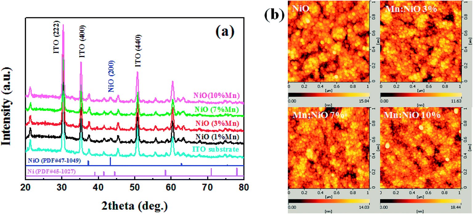 | ||
| Fig. 1 (a) XRD patterns of ITO substrate and Mn-doped NiO films; (b) AFM images of undoped NiO and Mn-doped NiO films. | ||
The inset of Fig. 2(a) compares the optical transmittance spectra of the pure NiO and Mn:NiO films. Mn:NiO films at a low concentration also perform excellent transparency to visible light and the average optical transmittance value is about 80% which is close to that of pure NiO film. The transmittance is reduced to about 70% as the doping content increases to 10%. In addition, direct band gap NiO film obeys the following relation for high photon energies:
| (αhυ) ≈ A(hυ − Eg)1/2 | (1) |
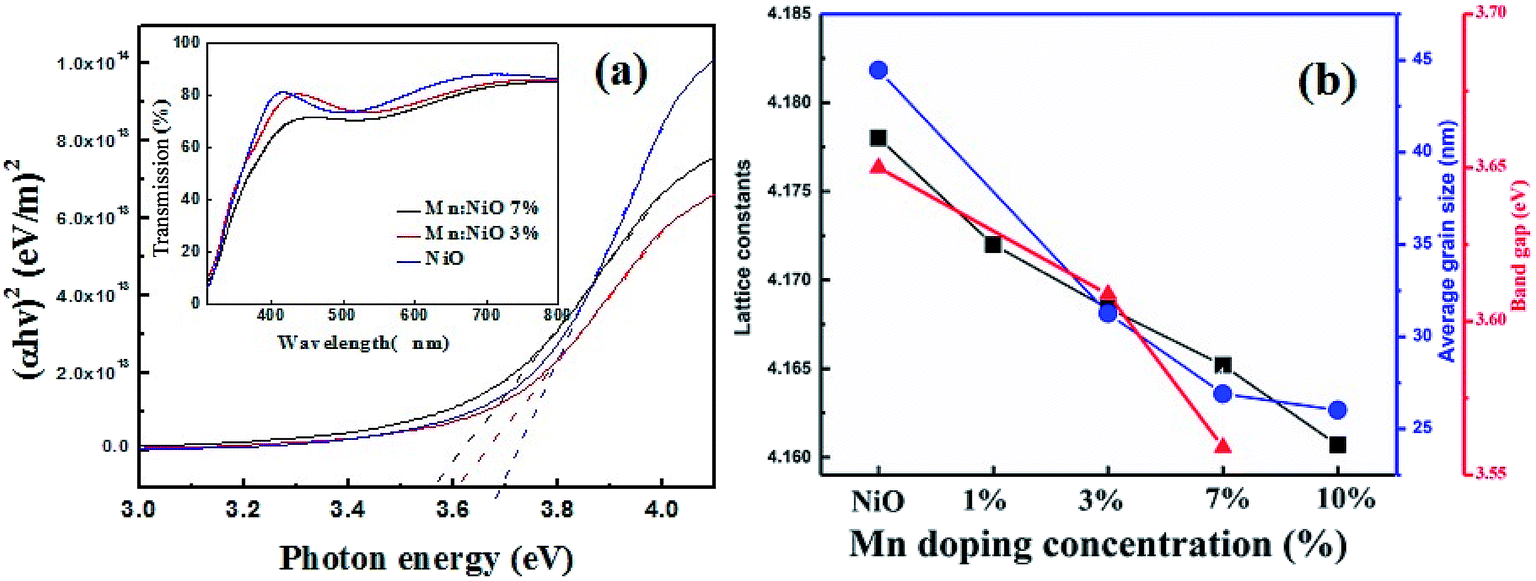 | ||
| Fig. 2 (a) Calculated band gap of Mn:NiO thin films in different doping concentration, the inset is their corresponding optical transmittance spectra; (b) relationship between the lattice constants, average grain size, band gap and Mn doping concentration. | ||
A schematic of Al/NiO/ITO device is presented in Fig. 3(a), with a sweeping voltage applied to the ITO bottom electrode to Al top electrode while the ITO bottom electrode is grounded. Fig. 3(b) shows the initial leakage current of the Al/Mn:NiO/ITO in different doping concentration. The initial resistance decreases with the doping content. Fig. 3(c) demonstrates the electroforming process with compliance current (CC) of 1 mA for the samples with different doping concentration. With the increase of the applied voltage from 0 V, the electroforming process occurs at high positive voltage (forming voltage). An abrupt current increasing activates the memory device from high resistance state (HRS) to low resistance state (LRS), and conductive filaments can be formed. It can be found that electroforming voltage remarkably reduces with the increasing percentages of doping concentration, as shown in Fig. 3(d). It also indicates that defect concentration is helpful to the formation of conductive filaments.
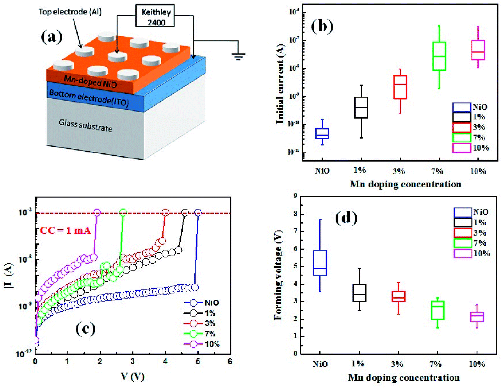 | ||
| Fig. 3 (a) Schematic of Al/Mn:NiO/ITO devices for measurement; (b) statistical results of initial leakage current (@0.5 V) of the Al/Mn:NiO/ITO based on 20 devices in different doping concentration; (c) electroforming curves of the Al/Mn:NiO/ITO devices in different doping concentration; (d) statistical results of electroforming voltage of the Al/Mn:NiO/ITO based on 20 device in different doping concentration. | ||
Fig. 4(a) shows typical BRS of I–V curve of NiO film without doping after electroforming process, and the bias direction is 0 V → negative → positive → 0 V as indicated by arrows. When the negative voltage increases from 0 V, the device is transformed from LRS to HRS at about −3.4 V, which is called as reset process. Subsequently, with the sweeping the voltage reversely, the device returned to LRS at about 4.1 V, which is called as set process. According to conductive filaments mechanism, the switching process can be accomplished by the migration/diffusion of oxygen vacancies, and the switching voltages were called as threshold voltages. The switching polarity can be easily understood based on the switching mechanism that set/reset processes reflect the growth/rupture of conductive filaments. Effect of Mn doping concentration in NiO films on BRS behaviors is demonstrated in Fig. 4(b). Analogous stable BRS behaviors are observed in all of the samples. It can be found that the threshold voltages decrease as the Mn doping concentration increases, as show in Fig. 4(c) and (d). The 10% Mn-doped NiO film performs the lowest threshold voltages below 1.5 V. It could be due to increasing ionic conductivity of oxygen vacancies, which can be modulated by Mn-doped defects.19,24 The defects caused by doping Mn and lower formation energy of Mn–O compounds facilitate the formation of oxygen vacancy, which is helpful to the formation of conductive filaments.25 Similarly, doping with trivalent impurity into ZrO2 and HfO2 can provide the initially high concentration of oxygen vacancies.26 In addition, the formation of conductive filaments is easy to grow along the grain boundary.27,28 The images of AFM show a significantly reduced grain size after doping, meaning a great increase in the density of grain boundaries. It can prominently drive the movement of oxygen vacancy. Furthermore, Mn-doping also improves the stability of threshold voltages while a larger dispersion can be found in the pure samples.
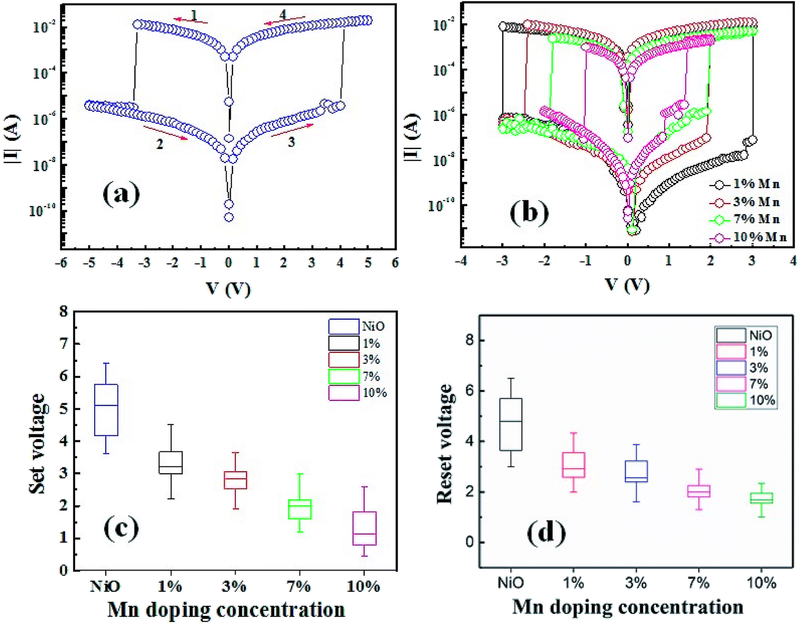 | ||
| Fig. 4 (a) I–V hysteretic curve of undoped NiO film; (b) comparison of BRS curves of Al/Mn:NiO/ITO device in different doping concentration; (c and d) statistical results of set/reset voltages of the Al/Mn:NiO/ITO based on 20 devices in different doping concentration. | ||
Fig. 5(a) compares the relationship between Mn doping concentration and the resistance at HRS, and ON/OFF ratio. Different from the monotonic trend with increased doping content for initial resistance, forming voltage, set voltage and reset voltage, the largest ON/OFF ratio (read at 1 V) reaches 106 for the 1% doped thin film, which is enhanced by two orders of magnitude compared with undoped film. It could be due to the difference between the initial state and HRS because of their different distribution state of oxygen vacancies. In addition, excessive defects in the case of higher doping concentration decrease the resistance at HRS. Furthermore, the retention properties of undoped and 1% Mn-doped NiO samples over 104 s without degeneration by sweeping model are shown in Fig. 5(b) and (c). Meanwhile the doped device also shows stable cycling property over 100 cycles, indicating the good reproducibility (Fig. 5(d)).
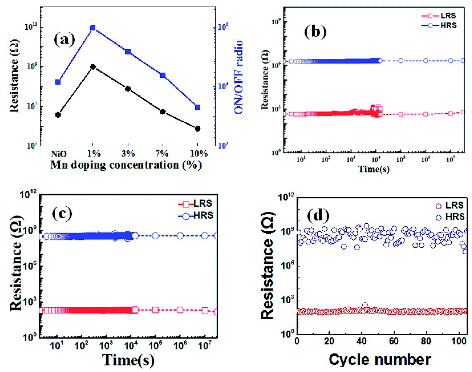 | ||
| Fig. 5 (a) Relationship between Mn doping concentration and the resistance at HRS, and ON/OFF ratio (read at 1 V) (b) retention data of undoped device, (c) retention data and (d) cycling characteristics of the Al/1% Mn:NiO/ITO. The dashed lines in (b) and (c) are extrapolated by the fitting data of linear function. | ||
To achieve further understanding of the mechanism of the typical BRS behaviors, the current conduction mechanisms of the LRS and HRS should be understood. Two linear fitting curves of undoped and doped NiO are separately depicted in Fig. 6(a) and (b). Both of undoped and doped NiO exhibit similar conduction behaviors. At LRS, the linearity curves with the slopes of almost 1 indicate ohmic conduction behavior, which is typically due to the formation of conductive filaments in Mn:NiO films. However, at the HRS, the I–V characteristic was more complicated and could be divided into two parts. At low voltages, the I–V curve was linear with slope about 1.3, corresponding to the ohmic mechanism region. At high voltages, the slope was increased close to 2, indicating that the conduction mechanism is dominated by trap-limited space charge-limited current conduction. The same results can also be fitted as the negative bias is applied. In our previous work, resistive switching modes can be tuned by the CC of electroforming and switching in the Al/NiO/ITO devices.21 It can be ascribed to Joule heating filament mechanism. For the BRS behavior obeying the mechanism, strong asymmetric I–V curve can be found. In addition, HRS at high voltage seems to be governed by Poole–Frenkel emission that involves thermal effect and trap sites. For the nonlinear BRS, it is dominated by oxygen vacancy drift induced by electric field across the interface between electrodes and NiO.8 In the two cases, dual-oxygen reservoir structure composed of Al/NiO interfacial layer and ITO should play an important role. But it should be ascribed to bulk properties associated with defects in this work, which is also confirmed by easier formation/rupture of conductive filaments at high doping concentration.
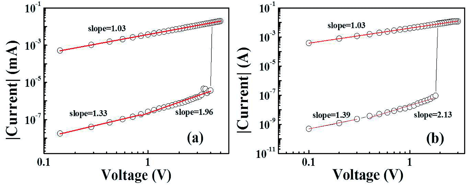 | ||
| Fig. 6 log(I)–log(V) curves of undoped (a) and 3% doped (b) NiO films. | ||
4. Conclusion
The BRS behaviors of Al/Mn:NiO/ITO device were investigated with different Mn doping concentration. The decreased electroforming voltage and threshold voltages have been found. Excellent BRS characteristics with enlarged ON/OFF ratio, good retention and stable cycling properties can be obtained at a low Mn-doped concentration. However, a lower ON/OFF ratio was presented in higher doping concentration. These results demonstrated that appropriate Mn doping can improve the BRS characteristics of NiO thin films including ON/OFF ratio, power consumption, and stability.
Conflicts of interest
There are no conflicts to declare.Acknowledgements
This work was supported by National Natural Science Foundation of China (Grant No. 51772252), and the Program for Young Science and Technology Innovation Team of Sichuan Province (2017TD0020).References
- R. Waser, R. Dittmann, G. Staikov and K. Szot, Adv. Mater., 2009, 21, 2632 CrossRef.
- J. J. Yang, F. Miao, M. D. Pickett, D. A. A. Ohlberg, D. R. Stewart, C. N. Lau and R. S. Williams, J. Nanotechnol., 2009, 20, 215201 CrossRef PubMed.
- F. Pan, S. Gao, C. Chen, C. Song and F. Zeng, Mater. Sci. Eng., R, 2014, 83, 1 CrossRef.
- C. Ye, J. J. Wu, G. He, J. Q. Zhang, T. F. Deng, P. He and H. Wang, J. Mater. Sci. Technol., 2016, 32, 1 CrossRef.
- X. L. Shao, L. W. Zhou, K. J. Yoon, H. Jiang, J. S. Zhao, K. L. Zhang, S. J. Yoo and C. S. Hwang, Nanoscale, 2015, 7, 11063 RSC.
- H. J. Kim, Y. J. Baek, Y. J. Choi, C. J. Kang, H. H. Lee, H. M. Kim, K. B. Kim and T. S. Yoon, RSC Adv., 2013, 3, 20978 RSC.
- T. Guo, T. Tan, Z. Liu and Z. Wu, RSC Adv., 2016, 6, 35740 RSC.
- X. C. Yuan, X. H. Wei, B. Dai and H. Z. Zeng, Appl. Surf. Sci., 2016, 362, 506 CrossRef.
- H. W. Zhang, L. F. Liu, B. Gao, Y. J. Qiu, X. Y. Liu, J. Lu, R. Q. Han, J. F. Kang and B. Yu, Appl. Phys. Lett., 2011, 98, 042105 CrossRef.
- C. Y. Liu, X. J. Lin, H. Y. Wang and C. H. Lai, J. Appl. Phys., 2010, 49, 056507 CrossRef.
- Y. Wang, Q. Liu, H. B. Lu, S. B. Long, W. Wang, Y. T. Li, S. Zhang, W. T. Lian, J. H. Yang and M. Liu, Chin. Sci. Bull., 2012, 57, 1235 CrossRef.
- Q. Liu, S. B. Long, W. Wang, S. Tanachutiwat, Y. T. Li, Q. Wang, M. H. Zhang, Z. L. Huo, J. N. Chen and M. Liu, IEEE Electron Device Lett., 2010, 31, 1299 Search PubMed.
- J. P. Han, P. Q. Mantas and A. M. R. Senos, J. Eur. Ceram. Soc., 2002, 22, 49 CrossRef.
- W. J. Jie, J. Zhu, W. F. Qin, X. H. Wei, J. Xiong, Y. Zhang, A. Bhalla and Y. R. Li, J. Phys. D: Appl. Phys., 2007, 40, 2854 CrossRef.
- J. Z. Huang, Y. Wang, Y. Lin, M. Li and C. W. Nan, J. Appl. Phys., 2009, 106, 063911 CrossRef.
- X. L. Wang, Q. Shao, C. W. Leung and A. Ruotolo, J. Appl. Phys., 2013, 113, 17C301 CrossRef.
- Y. C. Yang, F. Pan and F. Zeng, New J. Phys., 2010, 12, 023008 CrossRef.
- X. H. Wu, Z. M. Xu, F. Zhao, X. H. Xu, B. B. Liu, T. Y. Sun, S. S. Liu, W. N. Zhao and Z. C. Ma, J. Alloys Compd., 2014, 602, 175 CrossRef.
- J. M. Luo, H. N. Zhang, J. P. Wen and X. D. Yang, J. Sol-Gel Sci. Technol., 2016, 78, 166 CrossRef.
- L. Goux, J. G. Lisoni, M. Jurczak, D. J. Wouters, L. Courtade and C. Muller, J. Appl. Phys., 2010, 107, 024512 CrossRef.
- X. C. Yuan, J. L. Tang, H. Z. Zeng and X. H. Wei, Nanoscale Res. Lett., 2014, 9, 268 CrossRef PubMed.
- M. Q. Guo, Y. C. Chen, C. Y. Lin, Y. F. Chang, B. Fowler, Q. Q. Li, J. Lee and Y. G. Zhao, Appl. Phys. Lett., 2017, 110, 233504 CrossRef.
- S. Nandy, U. N. Maiti, C. K. Ghosh and K. K. Chattopadhyay, J. Phys.: Condens. Matter, 2009, 21, 115804 CrossRef PubMed.
- C. H. Yang, J. Seidel, S. Y. Kim, P. B. Rossen, P. Yu, M. Gajek, Y. H. Chu, L. W. Martin, M. B. Holcomb, Q. He, P. Maksymovych, N. Balke, S. V. Kalinin, A. P. Baddorf, S. R. Basu, M. L. Scullin and R. Ramesh, Nat. Mater., 2009, 8, 485 CrossRef PubMed.
- S. Mondal, H. Y. Chen, J. L. Her, F. H. Ko and T. M. Pan, Appl. Phys. Lett., 2012, 101, 083506 CrossRef.
- A. N. Mikhaylov, E. G. Gryaznov, A. I. Belov, D. S. Korolev, A. N. Sharapov, D. V. Guseinov, D. I. Tetelbaum, S. V. Tikhov, N. V. Malekhonova, A. I. Bobrov, D. A. Pavlov, S. A. Gerasimova, V. B. Kazantsev, N. V. Agudov, A. A. Dubkov, C. M. M. Rosário, N. A. Sobolev and B. Spagnolo, Phys. Status Solidi C, 2016, 13, 870 CrossRef.
- M. Lanza, K. Zhang, M. Porti, M. Nafria, Z. Y. Shen, L. F. Liu, J. F. Kang, D. Gilmer and G. Bersuker, Appl. Phys. Lett., 2012, 100, 123508 CrossRef.
- C. B. Pan, Y. F. Ji, N. Xiao, F. Hui, K. C. Tang, Y. Z. Guo, X. M. Xie, F. M. Puglisi, L. Larcher, E. Miranda, L. L. Jiang, Y. Y. Shi, I. Valov, P. C. McIntyre, R. Waser and M. Lanza, Adv. Funct. Mater., 2017, 10, 1604811 CrossRef.
| This journal is © The Royal Society of Chemistry 2018 |