
 Open Access Article
 This Open Access Article is licensed under a Creative Commons Attribution-Non Commercial 3.0 Unported Licence
Development of a superhydrophobic electrospun poly(vinylidene fluoride) web via plasma etching and water immersion for energy harvesting applications†
Beom-Jun Jua,
Ji-Hyun Oha,
Changsang Yunb and
Chung Hee Park *a
*a
aDepartment of Textiles, Merchandising and Fashion Design, Seoul National University, Seoul, 08826, Republic of Korea. E-mail: junghee@snu.ac.kr
bDepartment of Fashion Industry, Ewha Womans University, Seoul, 03760, Republic of Korea
First published on 14th August 2018
Abstract
Smart textiles have been enormously developed recently, but attachment of batteries and low washing resistance are the major challenges in the development of wearable smart textiles. However, piezoelectric materials harvesting energy from mechanical action can be readily integrated with smart textiles and can replace conventional batteries. Therefore, energy harvesters with poly(vinylidene fluoride) (PVDF) were fabricated by the electrospinning process. In addition, simple CF4 plasma etching followed by water immersion of the electrospun PVDF webs resulted in superhydrophobicity, with a water contact angle of 169.8 ± 1.5°, a water shedding angle of 4.7 ± 1.8°, and self-cleaning properties. This would decrease the number of washing cycles during use and increase the durability of the smart textile. X-ray photoelectron spectroscopy indicated that metals were co-deposited as etch-resisting masks to fabricate a nanostructure during plasma etching and were removed by water immersion. The piezoelectric performance of the superhydrophobic electrospun PVDF web showed a higher peak-to-peak output voltage of 3.50 V than the untreated electrospun PVDF web (2.86 V). Furthermore, the breathability of the superhydrophobic PVDF web was remarkably higher than those of the PVDF film. Therefore, the new flexible electrospun PVDF web with superhydrophobicity and piezoelectricity has significant potential as energy harvesters in wearable smart textiles.
Introduction
Smart textiles, which have undergone tremendous growth recently, are defined as textiles such as fibers and filaments, yarns together with woven, knitted or non-woven structures, which can actively sense, react, actuate, and adapt their behaviors according to the change in environment.1,2 Through rapid development, smart textiles could be applied in various applications such as wearable devices, biomedical devices, and so on.3 Most smart textiles are powered by conventional rechargeable batteries; but there are limitations to integrate them fully with textiles. To be specific, traditional batteries such as lithium-ion batteries have concerns about safety relating to ignition and explosion of the consisting elements by external forces because of human motion.4 In addition, conventional batteries are hard and bulky to integrate with flexible structures.5 Thus, there is an increasing demand for flexible energy harvesters in order to withstand mechanical stress and strain originating from human body movements such as bending, twisting and stretching.6 Furthermore, some commercial smart textiles require removal of all electronic components for washing or need waterproof packaging to protect sensitive electronics from damage by water. Therefore, two main challenges need to be overcome for smart textile development: power supplies and low washing durability.5Piezoelectric materials have been widely used in the design of sensors, actuators, resonators, accelerometers, microphones, and acoustical memory devices for entertainment, health monitoring, and wireless communication.6,7 As a piezoelectric material, especially, poly(vinylidene fluoride) (PVDF) has great potential for use in wearable energy harvesting textiles, because PVDF can be easily combined with flexible textile structures.8 Thus, PVDF, exhibiting synergetic effects of flexibility and piezoelectric properties, is expected to be very useful for the fabrication of self-powered smart textiles.
Piezoelectricity is a coupling between mechanical and electrical energy in certain types of crystals. The piezoelectric PVDF polymer exhibits five crystalline phases: α, β, γ, δ, and ε corresponding to different chain conformations, viz. TTT (all trans) planar zigzag for β-phase, TGTG (trans–gauche–trans–gauche) for α and δ-phases and T3GT3G for γ and ε-phases.9 The β-phase exhibits the highest dipolar moment per unit cell, which is crucial to piezoelectric properties, when compared to the other phases.10
The most common method to obtain β-phase of PVDF is uni- or biaxial drawing of originally α-phase PVDF films with application of an electric field on both sides. Mechanical drawing causes the transition into a crystalline structure, which the polymer chains are forced to the most extended conformation. Then, high voltage of electrical field allows them to be oriented to crystalline polar axis along the field direction.11–13 Additionally, in casting processes, when controlling the evaporation rate of the solvent, the polar β-phase could be achieved by crystallization of PVDF.14,15 Many techniques have been utilized to obtain polar β-phase in PVDF materials by using particles such as CoFe2O4,16,17 NiFe2O4,16,17 BaTiO3,18 nano-clays,19 hydrated ionic salts,20 silicate,21 PMMA22 and anisotropic nanostructures23 that are proposed for the nucleation of β-phase PVDF in composites. By using these methods, the electrostatic interaction between the charged surface of the particles and the polar groups in PVDF chains such as CH2 and CF2 groups induces locally oriented dipoles. These are packed in TTT configuration, which means the formation of β-phase PVDF during crystallization.16,23 Electrospinning process can also provide piezoelectricity by β-phase of PVDF.24–26 The polar β-phase of PVDF is formed via physical and electrostatic forces applied to the polymer solution during the electrospinning process. The employed high voltage or high stretching ratio of the polymer solution jet enables formation of β-phase PVDF through crystallization. Therefore, the electrospinning process can be efficiently used to prepare piezoelectric PVDF nanofibers without further treatments such as poling.27 In addition, the electrospun webs have advantages of breathability due to their porous structures, and the possible enhancement of anti-wetting property by minimizing the contact area with a liquid drop because of nano-scale roughness introduced by the nanofibers.28
Piezoelectric polymers, such as PVDF or poly(vinylidene fluoride–trifluoroethylene) (PVDF–TrFE) that is widely known as a co-polymer of PVDF, have recently been actively researched as a nanogenerator for energy harvesting.29–31 Furthermore, particles of inorganic ceramics such as ZnO,32 PZT,33 BaTiO3![[thin space (1/6-em)]](https://www.rsc.org/images/entities/char_2009.gif) 25 and (Na,K)NbO334 have been mixed for the fabrication of piezoelectric composites in order to increase the electrical output when subjected to mechanical stimulation. However, all these studies have not considered water repellency and washing resistance of the piezoelectric materials. As for wearable devices, especially those using smart textiles, not only the self-powering system but also superhydrophobicity and self-cleaning effect are important, because water causes failure and degradation of piezoelectric devices because of electrolysis reaction.35 Therefore, it is important to improve the water repellency of wearable devices.
25 and (Na,K)NbO334 have been mixed for the fabrication of piezoelectric composites in order to increase the electrical output when subjected to mechanical stimulation. However, all these studies have not considered water repellency and washing resistance of the piezoelectric materials. As for wearable devices, especially those using smart textiles, not only the self-powering system but also superhydrophobicity and self-cleaning effect are important, because water causes failure and degradation of piezoelectric devices because of electrolysis reaction.35 Therefore, it is important to improve the water repellency of wearable devices.
Superhydrophobic surfaces exhibit a water contact angle (WCA) larger than 150° and a water shedding angle (WSA) less than 10°,36,37 resulting in easy removal of soils from these surfaces via rolling of water droplets. This phenomenon is called self-cleaning effect and can be implemented by using low surface energy surfaces and hierarchical structures consisting of dual-scale roughness. Superhydrophobic surfaces have been fabricated by dip-coating, spray-coating, sol–gel methods, layer by layer assembly, chemical vapor deposition, etc.38–42 However, all these techniques include complicated procedures and additional coating processes with low surface energy materials.
In this study, we aimed to develop the flexible and breathable electrospun PVDF web with both piezoelectricity and superhydrophobicity for smart textiles by a simple process, plasma etching and water immersion, without any additional coatings. Electrospinning was carried out to have not only the piezoelectric properties by the formation of β-phase of PVDF, but also the enhancement of breathability and hydrophobicity due to the introduction of PVDF nanofibers. Furthermore, the electrospun PVDF web was etched by tetrafluoromethane (CF4) plasma to form an additional nanostructure on the preliminary roughness by PVDF nanofibers. Then, the electrospun PVDF web with hierarchical roughness was immersed in water to lower the surface energy. It was intended that without any hydrophobic coating, the nanostructured electrospun PVDF webs exhibited superhydrophobicity as well as piezoelectricity, which could resolve the issues of power supplies and washing durability in the development of smart textiles. The piezoelectricity and the wettability were analyzed by measuring the output voltage, and the WCA and WSA, respectively. The morphology of the surface was observed using a field emission scanning electron microscope (FE-SEM). The chemical composition and the crystallinity were analyzed by X-ray photoelectron spectroscopy (XPS) and X-ray diffraction (XRD), respectively. Finally, air permeability and water vapor transmission rate (WVTR) were examined to evaluate the breathability of the electrospun PVDF web for use as clothing textiles in practical applications.
Experimental section
Material
Poly(vinylidene fluoride) (pellet, Mw: ∼275000, Sigma Aldrich, USA) was used as the main material for electrospinning. A poled PVDF film (40 μm, Piezotech, France) was purchased to compare its piezoelectricity with that of the electrospun PVDF web. N,N-dimethylformamide (DMF) and acetone provided by Daejung Chemicals, Korea were used as solvents. All chemicals were used without further purification.
Preparation of electrospun PVDF web
The PVDF pellets (25 wt%) were dissolved in a mixture of DMF/acetone in the volume ratio of 7:3 by mixing with a magnetic stirring bar for 2 h at 70 °C. Subsequently, ultrasonic treatment was performed for 30 min to obtain a homogeneous transparent solution prior to the electrospinning process. For electrospinning, the dissolved PVDF solution was placed into a 10 mL syringe equipped with a 22 G blunt end needle. A metallic collector, which rotated at 100 rpm, was covered with an aluminium foil and placed 12.5 cm away from the tip of the needle. The voltage applied between the needle and the collector was 18 kV, and the solution flow rate was 1.2 mL h−1. The electrospinning process was conducted for 3 h at 24 ± 2 °C and 10 ± 5% relative humidity (RH). The obtained electrospun PVDF webs were cured in a vacuum oven at 70 °C for 12 h to remove the remaining solvent. The detail conditions of electrospinning mentioned above were set in order to fabricate uniform PVDF nanofibers having higher piezoelectric performance according to general processing methods as shown in Table S1.†30,43
Surface modification of electrospun PVDF web
Plasma etching followed by water immersion were conducted to render superhydrophobic surfaces, as shown schematically in Fig. 1. The electrospun PVDF webs were covered with a 250 mesh per inch twill weave stainless steel (SUS304) mesh as a metal source and then etched with CF4 plasma by using a reactive ion etching equipment (RIE 80Plus, Oxford instrument, UK). The plasma power and the substrate bias voltage were 180 W and −500 V, respectively. The flow rate of the CF4 gas and operating pressure were maintained at 20 sccm and 40 mTorr, respectively. The etching durations were set to 5, 10, 15, 20, and 30 min. The base pressure in the chamber was less than 0.5 mTorr. Subsequently, the plasma etched electrospun PVDF webs were immersed in deionized water for 30 s and dried in an oven at 70 °C for 10 min. The sample codes corresponding to the different experimental conditions are provided in Table 1. | ||
| Fig. 1 Schematic illustration of the surface modification process of the superhydrophobic electrospun PVDF web. | ||
| Code | Description |
|---|---|
| UT | Untreated electrospun PVDF web |
| P5-30 | Electrospun PVDF web with plasma etching for 5–30 min |
| P5-30W | Electrospun PVDF web with plasma etching for 5–30 min followed by water immersion |
Morphology
The changes in the surface morphology of the PVDF films and the electrospun webs after plasma etching followed by water immersion were observed using an FE-SEM (SUPRA 55VP/SIGMA, Carl Zeiss, Germany) at an acceleration voltage of 2.0 kV. The films and the electrospun webs were coated with a 10 nm-thick Pt film to make the samples conductive and avoid electron charge accumulation while imaging. The average diameter of the PVDF nanofibers, and the diameter and the aspect ratio of the nanostructures were calculated by measuring ten representative nanostructures using Image J (image analyzing software; National Institute of Health, USA).Crystallinity and chemical composition
X-ray diffraction patterns, to confirm the crystalline structures of PVDF, were obtained using an XRD analyzer (New D8 Advance, Bruker, USA) with Cu-Kα radiation at 40 kV and 40 mA. The XRD measurements were recorded in the 2θ range of 10 to 45°, and the scan speed and the scan size were 0.3° s−1 and 0.02°, respectively. The surface chemical composition and the bonding structure of the electrospun webs were investigated by X-ray photoelectron spectroscopy (XPS, AXIS-HSI, Kratos Analytical, UK) to explain the phenomenon of superhydrophobicity observed after plasma etching and water immersion.Mechanical properties
To analyze the effect of plasma etching on the mechanical properties, the tensile strength of the electrospun PVDF web was studied using a universal testing machine (Instron-5543, Instron, USA) with specimens sized at 50 × 20 × 0.06 mm3 according to ASTM D5035 strip method. The gauge speed was 10 mm min−1. The average value of tensile strength was obtained from five measurements.Wettability
The WCA of the electrospun PVDF webs was investigated using a contact angle goniometer (Theta Lite, Attension, Finland), and the deionized (DI) water droplet had a volume of 3.0 ± 0.2 μL. The average water contact angle was obtained by measuring the contact angle of the same sample at five different positions. We examined the self-cleaning performance by analyzing two properties: WSA and bouncing behavior of water droplets. The WSA was measured according to the method of Zimmermann et al.44 After releasing a water droplet with a volume of 12.5 ± 0.5 μL at a height of 1 cm, the minimum angle that the droplet rolled off the surface of the specimens for a distance of 2 cm was determined. The WSA values reported here are the average of five measurements. The bouncing behavior of the superhydrophobic electrospun PVDF web was recorded using a high-speed motion camera (NX3, IDT Vision, USA).Piezoelectricity
The piezoelectric properties of the PVDF film and the electrospun PVDF webs were determined as both of the output voltage and current using a nanovoltmeter (2182A, Keithley, USA) and galvanostat (IviumStat, Ivium technologies, Netherlands). Flexible nanogenerators were fabricated using an indium tin oxide (ITO) – polyethylene terephthalate (PET) substrate (Fine Chem., Korea) as a bottom electrode to detect the piezoelectric performance when a regular bending strain was applied onto the samples. The size of the substrate and the electrospun PVDF web were 30 × 80 mm2 and 25 × 40 mm2, respectively (Fig. 9a). The bending motion was performed manually until both sides of the nanogenerators were matched in half. The bending and releasing cycle was repeated with a frequency of 1 Hz. The peak-to-peak voltage and current were calculated as the piezoelectric response to compare the piezoelectricity of each sample according to the method of Liu et al.45Breathability
The breathability was evaluated using the WVTR and air permeability. The WVTR, which indicates the amount of water vapor passing through the web, was assessed using ASTM E96-80. An electrospun PVDF web with a diameter of 7 cm was placed on a water vapor permeability cup, which was pre-heated to a temperature of 40 ± 2 °C and filled with 33 g of anhydrous calcium chloride (Showa Chemical Co. Ltd, Japan) as a moisture absorbent. The cups were cured in a conditioned chamber at 40 ± 2 °C and 90 ± 5% RH for 1 h, and the weight of the cups was measured. The measured cups were placed in the conditioned chamber for another 1 h and then, the weight change was measured. The average amount of water vapor transmission per unit area for 24 h was calculated from three measurements. Air permeability, which denotes the volume of air passing through the electrospun PVDF webs, was tested according to ASTM D737-7515 using an air permeability tester (FX3300, TEXTEST, Switzerland) at a pressure of 125 Pa.Results and discussion
Morphology
The average diameter of the untreated PVDF nanofibers was 875 ± 150 nm. As shown in Fig. 2, the smooth surfaces of the untreated electrospun web were modified to form nanostructures after surface modification. Nanostructures on the surface of PVDF nanofibers were formed via co-deposition of metal compounds from a stainless steel mesh during CF4 plasma etching. This is because metal atoms such as Fe and Cr were sputtered from stainless steel during plasma etching and co-deposited on the surface as metal clusters. These clusters functioned as an etch-resisting mask because of the difference in the etch rate between the metal clusters and the PVDF nanofibers.46 Therefore, preferential etching on the surface of PVDF nanofibers induced by metal co-deposition caused the formation of nanostructures with a high aspect ratio. In addition, the surfaces of the PVDF film and the electrospun PVDF web were similarly etched to form nanostructures, as shown in Fig. S1b and d.† In the initial stage of metal co-deposition, as the etching duration was increased up to 15 min, the diameter of the nanostructures increased from 14.4 nm to 30.3 nm, which was maintained after 15 min (Fig. 2b–f). This can be explained by agglomeration of metal clusters during plasma etching.47,48 In addition, the height of the nanostructure significantly increased from 9.3 nm to 72.2 nm, so that the aspect ratio increased with increase in the etching duration. As a result, the aspect ratios were 0.64 ± 0.08, 0.65 ± 0.08, 1.16 ± 0.23, 2.26 ± 0.57, and 2.38 ± 0.47 for etching durations of 5, 10, 15, 20, and 30 min, respectively. The nanostructures that were created on the surface of the PVDF nanofibers were maintained after water immersion (Fig. S1†), giving rise to hierarchical structures, which are essential for superhydrophobicity. Although the aspect ratio of the nanostructure was higher at longer etching duration, decreased diameter and breakage of the PVDF nanofibers were observed after plasma etching for more than 20 min, as shown in Fig. S2.† Therefore, plasma etching of the PVDF web for 15 min was regarded as the optimum condition at which superhydrophobicity was achieved without significant damage of the nanofibers. | ||
| Fig. 2 High resolution SEM images of the electrospun webs after plasma etching for (a) 0, (b) 5, (c) 10, (d) 15, (e) 20, and (f) 30 min. All the samples were subsequently immersed in water. Each scale bar denotes 200 nm. | ||
Crystallinity and chemical composition
Fig. 3 shows the XRD patterns of the various PVDF samples. The presence of two peaks at 18.4 and 19.9° in the XRD pattern confirms α-phase crystal structure of the PVDF pellet. However, the PVDF film exhibited β-phase crystal structure, as evident from the peak at 20.6°.49 In case of the untreated electrospun PVDF web, the broad peak in the range of 19.9 to 20.6° indicates that the α-phase of the PVDF structure was partially converted to the β-phase owing to adequate stretching and application of high electric voltage during electrospinning; this is similar to the transition from α-phase to β-phase caused by mechanical drawing at T < 90 °C.11–13 However, the content of β-phase slightly decreased after CF4 plasma etching for 15 min and water immersion for 30 s.50,51 This can be explained by the increase in the local temperature above 100 °C on the surface of the electrospun PVDF nanofibers during plasma etching. This suggests that crystalline structures are easily changed from semi-crystalline β-phase to amorphous α-phase with increase in the segmental mobility of the PVDF chains.50,52,53 Nevertheless, the reduction in the content of the β-phase was so small that the content of β-phase was still sufficient to display the piezoelectric properties required for energy harvesting textiles.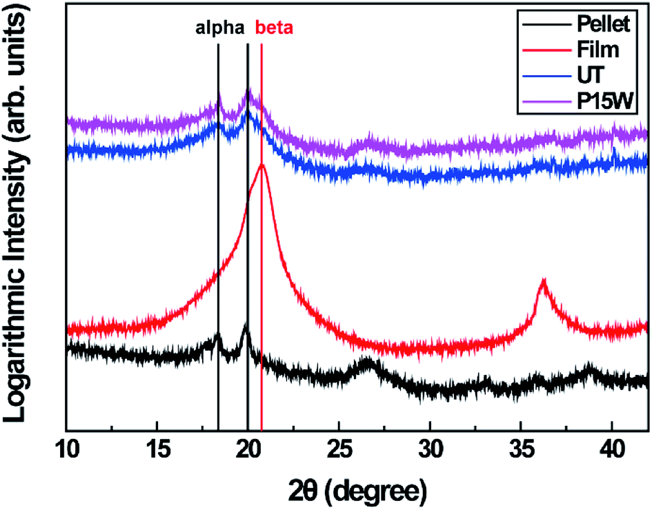 | ||
| Fig. 3 XRD spectra of the PVDF pellet, PVDF film, untreated electrospun PVDF web (UT), and electrospun PVDF web with plasma etching for 15 min followed by water immersion (P15W). | ||
To analyze the change in the chemical composition after plasma etching or water immersion, XPS analysis was performed. As shown in Fig. 4a, Fe and Cr atoms were detected on the surface of the electrospun PVDF web treated with only plasma etching for 15 min. The two peaks in the Fe 2p spectra from 705 to 735 eV correspond to Fe 2p1/2 and Fe 2p3/2, respectively (Fig. 4b). Additionally, peaks related to Cr 2p1/2 and Cr 2p3/2 are located at 587.5 and 577.3 eV, respectively.46,54 These results indicate that the metal clusters that played the role of an etch-resisting mask are introduced on the surface of the nanofiber during plasma etching, resulting in the formation of nanostructures.46
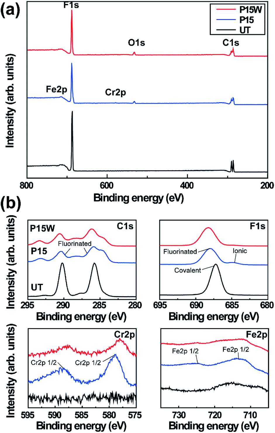 | ||
| Fig. 4 XPS spectra of the untreated electrospun PVDF web (UT), electrospun PVDF web with plasma etching for 15 min (P15), and electrospun PVDF web with plasma etching for 15 min followed by water immersion (P15W). (a) Wide survey scan and (b) high-resolution XPS spectra of C 1s, O 1s, Fe 2p, and Cr 2p. | ||
The XPS peaks corresponding to fluorine were also analyzed. Before plasma etching, the untreated electrospun PVDF web exhibited only one peak at 687.3 eV which corresponds to the covalent bond from (CH2–CF2). However, in comparison with that of the untreated electrospun PVDF web, the peak of the covalent F-bond in the plasma etched sample shifts by approximately +1.0 eV and broadens because of fluorination on the surface during plasma etching.55,56 Fluorination occurred with the formation of new F-bonded components, such as CHF–CF2 at 688.7 eV and CF2–CF2 or CF3 at 689.8 eV. Additionally, a peak at 684.2 eV, originating from the ionic-F bond, was observed, which is attributed to the formation of metal fluoride with an ionic bond between metal and fluorine. The peaks of C-bond shift from the peak of C–H bond at 286.7 eV and CH2–CF2 at 289.5 eV and broaden because of the fluorination which causes the formation of other components such as CHF–CH2 or CHF–CHF at 287.5 to 288.0 eV, CF2–CHF at 290.7 to 291.3 eV, CF2–CF2 at 292.3 eV, and CF3–CFx at 293.6 eV.57–59
After the water immersion, the metal compounds are mostly removed from the surface of the electrospun PVDF web. Consequently, the intensities of the peaks of Cr and Fe decrease and the atomic concentration of the metals become relatively low compared to that in the electrospun PVDF web only plasma etched for 15 min (Table 2). Furthermore, the intensity of the peak corresponding to the ionic-F bonds decreases after water immersion. These results represent that water immersion leads to the removal of hydrophilic metal fluoride through the hydrolysis reaction. This reaction could be confirmed by the reduction of pH value from neutral to acid. This change indicates that hydrofluoric acid (HF) was formed as a product of hydrolysis reaction in DI water, also the metal ions might exist at the same time.54,60,61 However, there was no significant change in the broadened peaks of the covalent bonds, as shown in Fig. 4b, which indicates that compositional changes due to fluorination might be not affected by water immersion. The peak corresponding to O-bond was detected not only in the sample with only plasma etching, but also in the sample with plasma etching followed by water immersion, which indicates that the remaining free radicals fabricated during plasma etching could be oxidized at ambient conditions.
| Sample code | Atomic concentration (at%) | ||||
|---|---|---|---|---|---|
| C | O | F | Cr | Fe | |
| UT | 50.58 | — | 49.42 | — | — |
| P15 | 50.95 | 3.22 | 44.96 | 0.35 | 0.51 |
| P15W | 50.94 | 4.43 | 44.35 | 0.14 | 0.14 |
Mechanical properties
The tensile strength was measured to analyze the effect of surface modification on the mechanical properties of the electrospun PVDF webs. The tensile strengths of all the plasma treated samples were tested after water immersion. The results, as shown in Fig. 5, indicate that the tensile strength of the electrospun PVDF webs decreases with increase in the etching duration. This is possibly because the average diameter of the fibers decreased with increase in the etching duration, and breakage of PVDF nanofibers was observed when the etching duration was longer than 20 min (Fig. S2†). Moreover, CF4 species such as cations, anions, and radicals, which are highly active to make a reaction with the substrate, could have attacked the C–C bond of the PVDF polymer chains during plasma etching.62 The breakage of the PVDF nanofibers and the formation of shorter PVDF polymer chains might have reduced the mechanical strength after a long duration of plasma etching.63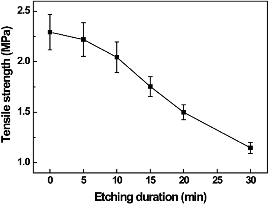 | ||
| Fig. 5 Tensile strength of the electrospun PVDF webs at different etching durations. | ||
Wettability
The WCA of the untreated electrospun PVDF web, 137.6 ± 1.9°, was significantly higher than that of the PVDF film, 82.9 ± 1.4°. Poly(vinylidene fluoride) is a kind of hydrophobic material; therefore, electrospun PVDF web showed increased hydrophobicity because of the formation of preliminary roughness by the PVDF nanofibers. The WCA of the electrospun PVDF web plasma etched for 15 min was 140.7 ± 2.3°, which is close to the WCA value of the untreated one. In addition, the WSAs of both the untreated and the plasma etched samples are still higher than 45°, as shown in Table 3. The metal mask on the surface during plasma etching is mainly composed of metal fluoride (FeF2, CrF2) formed by metal co-deposition from the stainless steel mesh. The metal fluorides have a very high surface energy, ranging from 174 to 241 dyne per cm,64,65 making the surface partially hydrophilic. However, hydrophobization, because of the fluorination by F atom radicals, simultaneously occurs during plasma etching. Therefore, the wettability of the electrospun PVDF web with only plasma etching was maintained owing to a counterbalance of the effect of metal co-deposition with that of fluorination.| Properties | Samples | |||
|---|---|---|---|---|
| PVDF film | Electrospun PVDF web | |||
| UT | P15 | P15W | ||
| WCA (°) |  |
 |
 |
 |
| 82.9 ± 1.4 | 137.6 ± 1.9 | 140.7 ± 2.3 | 169.8 ± 1.5 | |
| WSA (°) | >45 | >45 | >45 | 4.7 ± 1.8 |
To lower the surface energy, water immersion was performed for 30 s after plasma etching. The WCA of the electrospun PVDF web (P15W) drastically increased from 140.7 ± 2.3 to 169.8 ± 1.5°, and the WSA decreased from higher than 45 to 4.7 ± 1.8° (Table 3). Since water immersion promoted hydrolysis of metal fluoride compounds that have high surface energy, hydrophilic metal compounds were removed from the plasma etched electrospun PVDF webs during water immersion. Consequently, plasma etched and water immersed PVDF webs showed superhydrophobicity with the introduction of nanostructures on the surface of an intrinsically low surface energy (33.2 dyne per cm) material.66 Therefore, it is evident that plasma etching enables the formation of hierarchical roughness on the electrospun PVDF web, and the subsequent water immersion is necessary to lower the surface energy by eliminating the hydrophilic metal compounds from the surface.
To investigate the influence of etching duration on the wettability, the WCA and the WSA of the electrospun PVDF webs were measured at different etching durations. As shown in Fig. 6, the WCA of the electrospun PVDF web increases from 137.6 ± 1.9 to 171.1 ± 1.0° and the WSA decreases from higher than 45° to 4.6 ± 0.8° up to the etching duration of 20 min. The aspect ratio of the nanostructures on the surface of the PVDF nanofibers increased with increase in the etching durations (Fig. 2), leading to an increase in the level of hydrophobicity.67 If the aspect ratio of the nanostructures is adequately increased, the wetting state of a water droplet can be shifted from the Wenzel state to the Cassie–Baxter state, which is a critical wetting condition for fabricating a superhydrophobic surface.68,69 Based on these results, it is confirmed that a hierarchical structure and low surface energy are essential to achieve superhydrophobicity.68,70 Therefore, considering the increase in the superhydrophobicity and the degradation in the mechanical properties in accordance with the etching duration, the condition of plasma etching for 15 min followed by water immersion was considered as the optimum condition, with WCA of 169.8 ± 1.5° and WSA of 4.7 ± 1.8°. Hence, all subsequent superhydrophobic electrospun PVDF webs were fabricated by plasma etching for 15 min with water immersion to evaluate other properties.
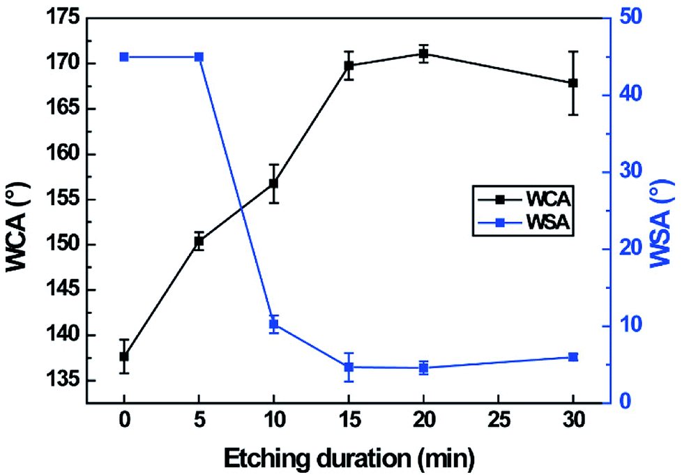 | ||
| Fig. 6 Variations of WCA and WSA of the electrospun PVDF webs with etching duration. All the samples were tested after water immersion. | ||
To simulate the water resistance of a raindrop on the surface of the superhydrophobic electrospun PVDF web, a water droplet impact test was conducted. As shown in Fig. 7a and b, the water droplet bounces on the surface of superhydrophobic electrospun PVDF web without leaving any residue, while the water droplet makes a finite contact angle and adheres to the surface of the untreated electrospun PVDF web. This bouncing behavior indicates that the superhydrophobic electrospun PVDF web has an excellent repellency to water. In addition, Fig. 7c shows the great repellency of the superhydrophobic electrospun PVDF web to various liquids that may be exposed to smart textiles during practical applications. The superhydrophobic electrospun PVDF web also displayed self-cleaning properties that allowed for the removal of contaminants from the surface via rolling of water droplets (Fig. 8). It is expected that the number of washing required for clothing could be reduced because of the superhydrophobic nature, and the developed superhydrophobic electrospun PVDF web could exhibit more durable piezoelectricity owing to the reduced number of washing cycles.
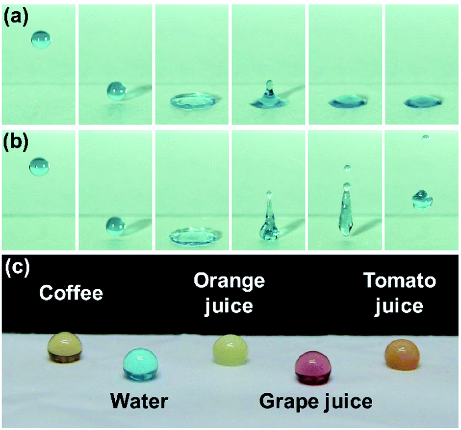 | ||
| Fig. 7 Bouncing behavior of water droplets on the surface of (a) the untreated PVDF web and (b) the superhydrophobic electrospun PVDF web. (c) Repellency of the superhydrophobic electrospun PVDF web to various liquids. | ||
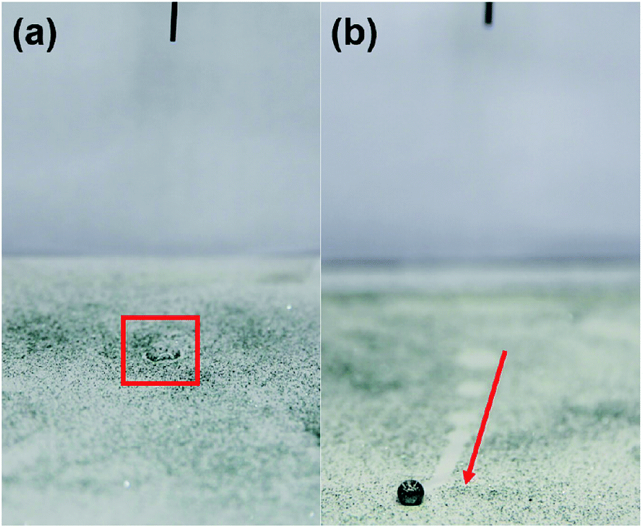 | ||
| Fig. 8 Self-cleaning properties of (a) the untreated electrospun PVDF web and (b) the superhydrophobic electrospun PVDF web contaminated with silicon carbide particles after dropping water droplets. | ||
Piezoelectricity
The piezoelectric performances of the PVDF film and the untreated and superhydrophobic electrospun PVDF webs under bending motion at a frequency of 1 Hz are shown in Fig. 9a. When a bending force was applied on the samples, the PVDF film generated a higher peak-to-peak output voltage, 4.51 V, than the untreated electrospun PVDF web, 2.68 V (Fig. 9b and c). This is because the PVDF film had a higher intensity of the β-phase peak (Fig. 3) and a higher area density (7.8 mg cm−2) than the electrospun PVDF web (2.1 mg cm−2). Also, a peak-to-peak output current showed a similar tendency that output current of the film, 343 nA, was higher than that of the untreated electrospun PVDF web, 191 nA (Fig. S3†).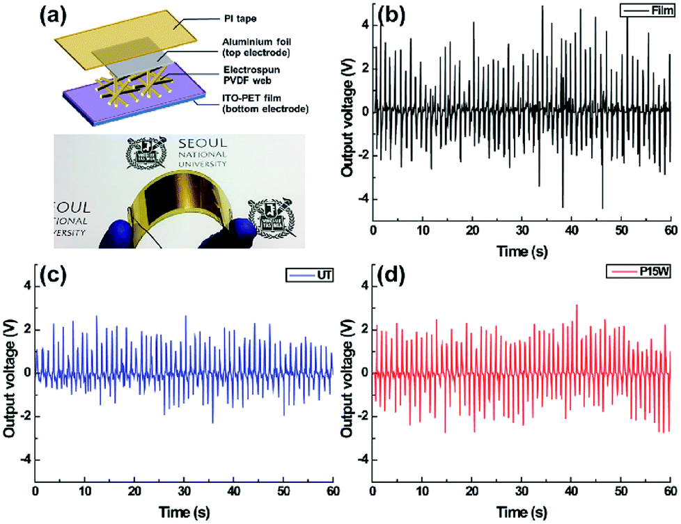 | ||
| Fig. 9 (a) Schematic and photograph of the nanogenerator consisting of the electrospun PVDF web, Al foil (top electrode), and ITO-PET film (bottom electrode). Output voltages of (b) the PVDF film, (c) the untreated electrospun PVDF web (UT), and (d) the electrospun PVDF web with plasma etching for 15 min followed by water immersion (P15W) under bending motion. | ||
The superhydrophobic electrospun PVDF web with plasma etching for 15 min followed by water immersion showed a peak-to-peak output voltage of 3.50 V, current of 241 nA, and an increase of approximately 30% in the piezoelectric performance in comparison with that of the untreated electrospun PVDF web, as shown in Fig. 9d and S3.† Even though the intensity of the β-phase peak slightly decreased after plasma etching and water immersion, the enhancement of piezoelectric response of the superhydrophobic electrospun PVDF web originated from the presence of nanostructures on the surface which led to an increase in the adhesion between electrodes and energy harvesters.71 Therefore, the superhydrophobic electrospun PVDF web with plasma etching for 15 min followed by water immersion had a much higher interface with electrodes than the smooth untreated electrospun PVDF and hence, showed an enhanced piezoelectric performance.71
Several researches reported the piezoelectric response of the nanogenerators based on electrospun PVDF nanofibers. The peak-to-peak output voltage and current were estimated by calculating twice as much as reported values. Some of the piezoelectric performance of previous studies are as follows: electrospun PVDF web (4.4 V/9 mA),72 composite of ZnO/PVDF (2.2 V),31 composite of BaTiO3/PVDF (0.6 V),25 composite of (Na,K)NbO3/PVDF (2.0 V/156 nA).34 Within our experimental condition, the superhydrophobic electrospun PVDF web showed enough piezoelectric performance (3.50 V/241 nA) without blending any piezoelectric ceramics. This result was the similar or improved level of piezoelectricity in comparison with that of the composites, because electrical output of the electrospun web strongly depends on the conditions of electrospinning.30 Furthermore, piezoelectric response could be changed by measuring methods including the intensity of impact force and the frequency of mechanical motions.72
Breathability
The breathability of the superhydrophobic electrospun PVDF web was investigated by measuring the air permeability and the WVTR, and the results are shown in Fig. 10. Compared to the PVDF film that does not have any pore structure, the electrospun PVDF web, with lots of nano-scale pores, exhibited a much higher air permeability and WVTR.28 The superhydrophobic electrospun PVDF web with plasma etching for 15 min followed by water immersion showed a similar air permeability and WVTR as those of the untreated electrospun PVDF web. These results imply that plasma etching took place only on the surface of electrospun web and did not have an effect on the bulk properties, maintaining the pore structures of the electrospun PVDF web.37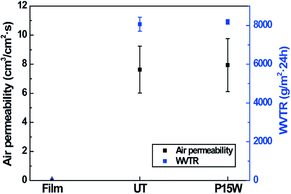 | ||
| Fig. 10 Air permeability and WVTR of the PVDF film, untreated electrospun PVDF web (UT), and electrospun PVDF web with plasma etching for 15 min followed by water immersion (P15W). | ||
Compared to the PVDF film, the air permeability and the WVTR were highly improved through electrospinning. In addition, the breathability of the superhydrophobic electrospun PVDF web was still maintained after surface modification. Based on these results, we can conclude that the newly developed superhydrophobic and piezoelectric electrospun PVDF web is more suitable in transmitting air and sweat than the PVDF film, and thus provides improved wearing comfort when applied in smart clothing materials.
Conclusions
Superhydrophobic and piezoelectric electrospun PVDF webs for energy harvesting were fabricated by CF4 plasma etching and water immersion without the deposition of any coating. By using a stainless steel mesh as an etch-resisting mask during plasma etching, nanostructures were formed through metal co-deposition. Subsequently, water immersion for 30 s was carried out to remove hydrophilic metal compounds. Plasma etching followed by water immersion is a very simple and eco-friendly method to obtain superhydrophobic surfaces without additional processes. Plasma etching of the electrospun PVDF web for 15 min followed by water immersion was determined as the optimum conditions, taking into account both mechanical properties and superhydrophobicity. After surface modification, the surface of the electrospun PVDF web showed superhydrophobicity, with a WCA of 169.8 ± 1.5° and a WSA of 4.7 ± 1.8°. In addition, the superhydrophobic electrospun PVDF web exhibited excellent bouncing behavior of water droplets and repellency to various liquids. The superhydrophobic electrospun PVDF also exhibited self-cleaning properties, which helps in resolving the issue of washing durability of smart textiles. The developed electrospun PVDF web exhibited enhanced piezoelectric properties after surface modification, with the peak-to-peak output voltage reaching up to 3.50 V, compared with the untreated electrospun PVDF web which showed a peak-to-peak output voltage of 2.68 V. This piezoelectric characteristic is a possible solution for future power supplies via conversion of mechanical energy from body motions to electrical energy. Furthermore, the superhydrophobic electrospun PVDF web showed much higher air permeability and WVTR than the PVDF film, which indicates the potential of the superhydrophobic PVDF web for smart clothing. Therefore, the newly developed breathable electrospun PVDF web with both superhydrophobicity and piezoelectricity can be widely applied as practical flexible energy harvesters in wearable devices by overcoming the issues of limited power supply and washing durability.Conflicts of interest
There are no conflicts to declare.Acknowledgements
This work was supported by the National Research Foundation of Korea (NRF) grant funded by the Korea government (Ministry of Science and ICT; Grant No. NRF-2016M3A7B4910940 and NRF-2018R1A2B6003526)References
- M. Stoppa and A. Chiolerio, Sensors, 2014, 14, 11957–11992 CrossRef PubMed.
- L. Van Langenhove and C. Hertleer, International Journal of Clothing Science and Technology, 2004, 16, 63–72 CrossRef.
- M. Zhou, M. S. H. Al-Furjan, J. Zou and W. Liu, Renewable Sustainable Energy Rev., 2018, 82, 3582–3609 CrossRef.
- H. Nishide and K. Oyaizu, Science, 2008, 319, 737–738 CrossRef PubMed.
- K. Cherenack and L. V. Pieterson, J. Appl. Phys., 2012, 112, 091301 CrossRef.
- H. Wu, Y. Huang, F. Xu, Y. Duan and Z. Yin, Adv. Mater., 2016, 28, 9881–9919 CrossRef PubMed.
- J. Zhang and S. A. Meguid, Semicond. Sci. Technol., 2017, 32, 043006 CrossRef.
- T. Dias, Electronic Textiles: Smart Fabrics and Wearable Technology, Elsevier, 2015 Search PubMed.
- P. Martins, A. C. Lopes and S. Lanceros-Mendez, Prog. Polym. Sci., 2014, 39, 683–706 CrossRef.
- H. M. G. Correia and M. M. D. Ramos, Comput. Mater. Sci., 2005, 33, 224–229 CrossRef.
- P. Sajkiewicz, A. Wasiak and Z. Goclowski, Eur. Polym. J., 1998, 35, 423–429 CrossRef.
- M. C. Branciforti, V. Sencadas, S. Lanceros-Mendez and R. Gregorio, J. Polym. Sci., Part B: Polym. Phys., 2007, 45, 2793–2801 CrossRef.
- R. Gregorio and E. M. Ueno, J. Mater. Sci., 1999, 34, 4489–4500 CrossRef.
- D. L. Chinaglia, R. Gregorio, J. C. Stefanello, R. A. Pisani Altafim, W. Wirges, F. Wang and R. Gerhard, J. Appl. Polym. Sci., 2009, 116, 785–791 Search PubMed.
- R. Gregorio and D. S. Borges, Polymer, 2008, 49, 4009–4016 CrossRef.
- P. Martins, C. M. Costa, M. Benelmekki, G. Botelho and S. Lanceros-Mendez, CrystEngComm, 2012, 14, 2807 RSC.
- P. Martins, C. M. Costa and S. Lanceros-Mendez, Appl. Phys. A, 2010, 103, 233–237 CrossRef.
- S. F. Mendes, C. M. Costa, C. Caparros, V. Sencadas and S. Lanceros-Méndez, J. Mater. Sci., 2011, 47, 1378–1388 CrossRef.
- D. R. Dillon, K. K. Tenneti, C. Y. Li, F. K. Ko, I. Sics and B. S. Hsiao, Polymer, 2006, 47, 1678–1688 CrossRef.
- M. Benz, W. B. Euler and O. J. Gregory, Macromolecules, 2002, 35, 2682–2688 CrossRef.
- J. Buckley, P. Cebe, D. Cherdack, J. Crawford, B. S. Ince, M. Jenkins, J. Pan, M. Reveley, N. Washington and N. Wolchover, Polymer, 2006, 47, 2411–2422 CrossRef.
- W. Ma, J. Zhang, S. Chen and X. Wang, Appl. Surf. Sci., 2008, 254, 5635–5642 CrossRef.
- M. S. Sebastian, A. Larrea, R. Gonçalves, T. Alejo, J. L. Vilas, V. Sebastian, P. Martins and S. Lanceros-Mendez, RSC Adv., 2016, 6, 113007–113015 RSC.
- J. Nunes-Pereira, V. Sencadas, V. Correia, J. G. Rocha and S. Lanceros-Méndez, Sens. Actuators, A, 2013, 196, 55–62 CrossRef.
- C. Lee, D. Wood, D. Edmondson, D. Yao, A. E. Erickson, C. T. Tsao, R. A. Revia, H. Kim and M. Zhang, Ceram. Int., 2016, 42, 2734–2740 CrossRef.
- B. S. Lee, B. Park, H. S. Yang, J. W. Han, C. Choong, J. Bae, K. Lee, W. R. Yu, U. Jeong, U. I. Chung, J. J. Park and O. Kim, ACS Appl. Mater. Interfaces, 2014, 6, 3520–3527 CrossRef PubMed.
- A. Gheibi, M. Latifi, A. A. Merati and R. Bagherzadeh, J. Polym. Res., 2014, 21, 1–7 Search PubMed.
- H. W. Ahn, S. E. Chung and C. H. Park, Text. Res. J., 2011, 81, 1438–1447 CrossRef.
- J. Serrado Nunes, A. Wu, J. Gomes, V. Sencadas, P. M. Vilarinho and S. Lanceros-Méndez, Appl. Phys. A, 2009, 95, 875–880 CrossRef.
- H. Shao, J. Fang, H. Wang and T. Lin, RSC Adv., 2015, 5, 14345–14350 RSC.
- G. Ico, A. Showalter, W. Bosze, S. C. Gott, B. S. Kim, M. P. Rao, N. V. Myung and J. Nam, J. Mater. Chem. A, 2016, 4, 2293–2304 RSC.
- M. S. Sorayani Bafqi, R. Bagherzadeh and M. Latifi, J. Polym. Res., 2015, 22, 1–9 CrossRef.
- J. S. Yun, C. K. Park, Y. H. Jeong, J. H. Cho, J. H. Paik, S. H. Yoon and K. R. Hwang, Nanomater. Nanotechnol., 2016, 6, 20 CrossRef.
- H. B. Kang, C. S. Han, J. C. Pyun, W. H. Ryu, C. Y. Kang and Y. S. Cho, Compos. Sci. Technol., 2015, 111, 1–8 CrossRef.
- W. P. Chen, H. L. W. Chan, F. C. H. Yiu, K. M. W. Ng and P. C. K. Liu, Appl. Phys. Lett., 2002, 80, 3587–3589 CrossRef.
- H. S. Kim and C. H. Park, RSC Adv., 2016, 6, 48155–48164 RSC.
- S. O. Kwon, T. J. Ko, E. Yu, J. Kim, M. W. Moon and C. H. Park, RSC Adv., 2014, 4, 45442–45448 RSC.
- J. Kim, H. S. Kim and C. H. Park, Text. Res. J., 2015, 86, 461–471 CrossRef.
- B. Leng, Z. Shao, G. d. With and W. Ming, Langmuir, 2009, 25, 2456–2460 CrossRef PubMed.
- L. Xu, W. Zhuang, B. Xu and Z. Cai, Appl. Surf. Sci., 2011, 257, 5491–5498 CrossRef.
- J. E. Mates, T. M. Schutzius, I. S. Bayer, J. Qin, D. E. Waldroup and C. M. Megaridis, Ind. Eng. Chem. Res., 2013, 53, 222–227 CrossRef.
- M. H. Shim, J. Kim and C. H. Park, Text. Res. J., 2014, 84, 1268–1278 CrossRef.
- C. Ribeiro, C. M. Costa, D. M. Correia, J. Nunes-Pereira, J. Oliveira, P. Martins, R. Goncalves, V. F. Cardoso and S. Lanceros-Mendez, Nat. Protoc., 2018, 13, 681–704 CrossRef PubMed.
- J. Zimmermann, S. Seeger and F. A. Reifler, Text. Res. J., 2009, 79, 1565–1570 CrossRef.
- Z. H. Liu, C. T. Pan, C. Y. Su, L. W. Lin, Y. J. Chen and J. S. Tsai, Sens. Actuators, A, 2014, 211, 78–88 CrossRef.
- T. J. Ko, K. H. Oh and M. W. Moon, Adv. Mater. Interfaces, 2015, 2, 1400431 CrossRef.
- X. Yu, P. M. Duxbury, G. Jeffers and M. A. Dubson, Phys. Rev. B: Condens. Matter Mater. Phys., 1991, 44, 13163–13166 CrossRef.
- A. L. Thomann, J. P. Rozenbaum, P. Brault, C. Andreazza-Vignolle and P. Andreazza, Appl. Surf. Sci., 2000, 158, 172–183 CrossRef.
- Alamusi, J. Xue, L. Wu, N. Hu, J. Qiu, C. Chang, S. Atobe, H. Fukunaga, T. Watanabe, Y. Liu, H. Ning, J. Li, Y. Li and Y. Zhao, Nanoscale, 2012, 4, 7250 RSC.
- D. M. Correia, C. Ribeiro, V. Sencadas, G. Botelho, S. A. C. Carabineiro, J. L. G. Ribelles and S. Lanceros-Méndez, Prog. Org. Coat., 2015, 85, 151–158 CrossRef.
- J. S. Lee, G. H. Kim, S. M. Hong, H. J. Choi and Y. Seo, ACS Appl. Mater. Interfaces, 2009, 1, 2902–2908 CrossRef PubMed.
- M. P. Silva, C. M. Costa, V. Sencadas, A. J. Paleo and S. Lanceros-Méndez, J. Polym. Res., 2011, 18, 1451–1457 CrossRef.
- V. Sencadas, S. Lanceros-Mendez, R. Sabater i Serra, A. Andrio Balado and J. L. Gomez Ribelles, Eur. Phys. J. E: Soft Matter Biol. Phys., 2012, 35, 41 CrossRef PubMed.
- E. K. Her, T. J. Ko, B. Shin, H. Roh, W. Dai, W. K. Seong, H. Y. Kim, K. R. Lee, K. H. Oh and M. W. Moon, Plasma Processes Polym., 2013, 10, 481–488 CrossRef.
- M. B. O. Riekerink, J. G. A. Terlingen, G. H. M. Engbers and J. Feijen, Langmuir, 1999, 15, 4847–4856 CrossRef.
- P. Montazer-Rahamati and F. A. J. Amouroux, Proceedings of the 10th International Symposium on Plasma Chemistry (ISPC-10), Bochum, Germany, 1991 Search PubMed.
- S. Sigurdsson and R. Shishoo, J. Appl. Polym. Sci., 1997, 66, 1591–1601 CrossRef.
- Y. Chul Woo, Y. Chen, L. D. Tijing, S. Phuntsho, T. He, J. S. Choi, S. H. Kim and H. K. Shon, J. Membr. Sci., 2017, 529, 234–242 CrossRef.
- A. Tressaud, E. Durand and C. Labrugère, J. Fluorine Chem., 2004, 125, 1639–1648 CrossRef.
- U. Mazurek, D. Schröder and H. Schwarz, Eur. J. Inorg. Chem., 2002, 1622–1634 CrossRef.
- A. L. Soli and R. H. Byrne, J. Solution Chem., 1996, 25, 773–785 CrossRef.
- X. Wei, B. Zhao, X. M. Li, Z. Wang, B. Q. He, T. He and B. Jiang, J. Membr. Sci., 2012, 407–408, 164–175 CrossRef.
- H. Savoji, S. Lerouge, A. Ajji and M. R. Wertheimer, Plasma Processes Polym., 2015, 12, 314–327 CrossRef.
- F. Aqra, J. Mol. Liq., 2014, 200, 120–121 CrossRef.
- S. Hara and K. Ogino, ISIJ Int., 1989, 29, 477–485 CrossRef.
- S. Park, J. Kim and C. H. Park, Text. Res. J., 2016, 87, 193–207 CrossRef.
- J. Brandrup and E. Immergut, Polymer handbook, Wiley, New York, 1998 Search PubMed.
- S. Park, J. Kim and C. H. Park, RSC Adv., 2016, 6, 45884–45893 RSC.
- J. Long, P. Fan, D. Gong, D. Jiang, H. Zhang, L. Li and M. Zhong, ACS Appl. Mater. Interfaces, 2015, 7, 9858–9865 CrossRef PubMed.
- J. H. Oh, T. J. Ko, M. W. Moon and C. H. Park, RSC Adv., 2017, 7, 25597–25604 RSC.
- T. Huang, C. Wang, H. Yu, H. Wang, Q. Zhang and M. Zhu, Nano Energy, 2015, 14, 226–235 CrossRef.
- J. Fang, X. Wang and T. Lin, J. Mater. Chem., 2011, 21, 11088 RSC.
Footnote |
| † Electronic supplementary information (ESI) available. See DOI: 10.1039/c8ra04652b |
| This journal is © The Royal Society of Chemistry 2018 |