
 Open Access Article
 This Open Access Article is licensed under a Creative Commons Attribution-Non Commercial 3.0 Unported Licence
Chitosan capped nickel oxide nanoparticles as a saturable absorber in a tunable passively Q-switched erbium doped fiber laser
Harith Ahmad†
 *,
Siti Aisyah Reduan and
Norazriena Yusoff
*,
Siti Aisyah Reduan and
Norazriena Yusoff
Photonics Research Center, University of Malaya, 50603 Kuala Lumpur, Malaysia. E-mail: harith@um.edu.my
First published on 18th July 2018
Abstract
Nickel oxide (NiO) nanoparticles successfully prepared from a nickel(II) chloride hexahydrate precursor are used to form a chitosan capped NiO nanoparticle thin film to serve as a saturable absorber (SA) for the generation of passively Q-switched pulses in an erbium doped fiber laser (EDFL). The NiO/chitosan SA based EDFL is able to generate stable pulsed outputs at a low threshold pump power of 104.90 mW with a central wavelength at 1562 nm. The highest pulse energy obtainable by the system is 15.30 nJ at a repetition rate of 42.66 kHz and a pulse duration of 2.02 μs. The laser has a spectral range of 58 nm from 1522 to 1580 nm, covering the C and L bands and even portions of the S band. This study experimentally demonstrates that the potential of the NiO/chitosan film as an SA material for Q-switching operations, combined with the biocompatibility, non-toxicity and high thermal resistance of Chitosan, holds great prospects for a broad range of applications.
Introduction
Q-switched and mode-locked fiber lasers are the focus of significant research efforts due to their ability to generate high peak powered outputs, in the range of tens of kilowatts to megawatts while at the same time retaining a compact and rugged form factor that is relatively easy and cost-effective to fabricate.1,2 Q-switched fiber lasers in particular are preferred for most practical applications, as even though the pulsed output generated is slower than that of mode-locked lasers, Q-switched lasers are still capable of generating pulses with significant peak powers.3,4 Additionally, Q-switched fiber lasers also do not require delicate adjustment and balancing of the dispersion and nonlinearity within the laser cavity as is usually the case with mode-locked fiber lasers, thus giving them an added advantage.5 These highly desirable traits have thus seen the integration of Q-switched fiber lasers into a multitude of real world applications such as range finding,6 medicine,7 micromachining,8 fiber optic sensing9 and telecommunications.10Q-switched pulses are typically generated through the use of a saturable absorber (SA), which modulates a continuous wave (CW) output into a periodic pulse train. For a long time, semiconductor saturable absorber mirrors (SESAMs) were the preferred choice of SA for generating Q-switched pulses in laser systems including fiber lasers and solid state lasers. However, SESAMs were bulky, fragile and expensive to fabricate, thus limiting their use to only applications in which they would be necessary. However, advances in materials science and fabrication techniques have now seen a new generation of SAs coming to the forefront. These new SAs, made from 2-dimensional (2D) and 3-dimensional (3D) materials such as carbon nanotubes (CNTs),11 graphene,12 topological insulators (TIs),13 transition metal dichalcogenides (TMDs),14 and black phosphorus15,16 have seen increasing use in various Q-switched fiber laser systems. SAs have also been used in solid state laser systems, as demonstrated by B. Xu et al., who fabricated an SA based on a few Bi2Se3 and MoS2 layers to generate Q-switched pulses in solid state lasers using Nd:LiYF4 (YLF) and Nd:YAIO3 crystals respectively.17,18
In this regard, transition metal oxide (TMO)-based SAs have now emerged as a new branch of SA capable materials19–21 with significant potential for inducing Q-switched pulses in fiber laser. This had been demonstrated by B. Xuekun et al.22 who used a ferro-oxide (Fe3O4) nanoparticle based SA for Q-switching operation in an erbium doped fiber laser (EDFL) cavity. The proposed laser generated pulses with energy of 23.67 nJ and width of 3.20 μs at a repetition rate of 33.30 kHz and peak power exceeding 110 mW. Additionally, J. Guo et al.23 demonstrated a passively Q-switched EDFL capable of generating an output with a pulse width as narrow as 1.15 μs and pulse energy as high as of 21.19 nJ at a repetition rate of 81.28 kHz using the SA fabricated from indium tin oxide (ITO) nanocrystals.
The aforementioned reports, along with other works,24–26 all indicate clearly the significant potential that TMOs based SAs have in the generation of pulsed outputs. Of the many TMOs explored for this application, nickel oxide (NiO) is seen to be a prime candidate for the development of SAs capable of generating Q-switched outputs. This is due primarily to the substantial electrical, mechanical and optical properties of NiO nanoparticles, which include a wide absorption band, low saturation intensity and fast response time.24,27 NiO nanoparticles also have significantly advantageous nonlinear photonic properties such as a good modulation depth, high optical damage threshold and low saturation intensity.28 These characteristics, combined with the relatively cost-effective and easy fabrication process of TMOs as SAs as well as its high chemical and thermal stability and environmentally friendly constitution,29 make it suitable for a variety of real world applications, including its usage in dye-sensitized solar cells,30 super capacitors,31,32 fiber and batteries33 and catalyst materials.34
In this work, NiO nanoparticles are synthesized and mixed with a polymer matrix to form thin films that are then used as SAs for generating a tunable Q-switched laser output from a C-band EDFL cavity. The sonochemical method is used to fabricate the NiO nanoparticles followed by a simple solution processing technique with chitosan to produce a NiO/chitosan thin film. Chitosan is chosen as the polymer host for the NiO nanoparticles due to its excellent film-forming capacity as well as high biocompatibility, good bioactivity, high biodegradability and non-toxicity as well as being readily available in abundance.35,36 The NiO/chitosan SA is then integrated into a C-band EDFL for the passive generation of Q-switched pulses. The NiO/chitosan based SA is expected to demonstrate a number of significant advantages, including low threshold pump power, broad wavelength tunability and high pulse generation stability that will make if significantly useful for real world applications.
Fabrication and characterization of nickel oxide/chitosan saturable absorber (SA)
For the synthesis of the NiO/chitosan thin film based SA, the following chemicals and reagents are first obtained. Nickel(II) chloride hexahydrate (NiCl2·6H2O) at purity of ≥97%, acetic acid at purity ≥ 99.8%, and sodium hydroxide (NaOH) are purchased from Sigma-Aldrich, while a 25% ammonia solution (NH3·H2O) is obtained from R&M Chemicals. High viscosity chitosan flakes is obtained from Fluka BioChemika. All reagents are of analytical grade and used as received without further purification.The NiO/chitosan film is synthesized by first preparing 1 M of Ni precursor by dissolving an appropriate amount of NiCl2·6H2O powder in 20 mL of distilled (DI) water while being stirred at room temperature. A 13 mL aqueous solution of NaOH (1 M) that functions as a structure-directing agent is added to the solution while the stirring continues. An NH3·H2O solution is then added drop-wise to maintain the pH of the solution at a value of approximately 10. Subsequently, the mixture is sonicated using probe type sonicator at 100 watt for 2 hours and the sonicated dispersions then centrifuged at 4000 rpm for 20 min to obtain black precipitates which are washed with DI water and ethanol several times to eliminate residual impurities. The precipitates are then dried at 60 °C in an oven for 24 hours to remove residual ethanol. To ensure that any remaining hydroxide forms of Ni are reduced to NiO, the black precipitate powder is annealed at 450 °C for 1 hour under atmospheric pressure.
The NiO/chitosan thin film is prepared by dispersing 50 mg NiO powder homogeneously in 10 mL of DI water using ultrasonication before being mixed with 10 mL of chitosan solution at the same concentration and being stirred at a temperature of 70 °C for a period of 1 hour. The chitosan solution itself is prepared by dissolving high viscosity chitosan flakes in 1% acetic acid while under constant stirring at room temperature for 5 hours to ensure the chitosan powder to be completely dissolved. The obtained slurry is poured into a Petri dish and dried in the oven at 60 °C until the desired NiO/chitosan film is formed. Fig. 1 shows the various key steps taken to form the NiO/chitosan thin film.
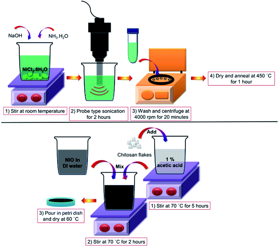 | ||
| Fig. 1 Schematic representation for: (top) the preparation of NiO nanoparticles using the sonochemical method and (above) the fabrication of the NiO/chitosan thin film. | ||
NiO/chitosan SA itself is fabricated by sandwiching a very small piece of the NiO/chitosan film between two single mode fiber ferrules using a fiber adaptor. A small amount of index matching gel is applied to the film and fiber ferrules to serve as an adhesive and at the same time used to minimize possible losses due to Fresnel reflection.
The crystalline phase of the nanoparticles is analyzed by a PANalytical Empyrean X-ray diffractometer (XRD) with monochromatized Cu Kα radiation and λ = 1.5418 Å. The system is operating at a scanning rate of 0.02° per second to over a 2θ range of 30° to 80°. Fourier transform infrared (FTIR) spectra analysis of the thin film is carried out using a Perkin Elmer FTIR-Spectrum 400 spectrometer at room temperature. A Field Emission Scanning Electron Microscope (FESEM) image is obtained by a Hitachi SU8220 operated at 1.0 kV while energy dispersive X-ray spectroscopy (EDX) analysis was carried out in conjunction with the FESEM analysis to confirm the material composition of the SA. Fig. 2 shows the XRD pattern for the NiO nanoparticles synthesized using the sonochemical method. Diffraction peaks are observed at 2θ values of 31.9°, 43.5°, 63.2°, 75.4° and 79.4°, and are assigned to the (1 1 1), (2 0 0), (2 2 0), (3 1 1) and (2 2 2) planes of NiO. These XRD peaks of NiO are consistent with the data of the JCPDS 47-1049 file, reflecting the formation of NiO after the reaction process.37 The sharp peaks indicate the high crystallinity of the NiO nanoparticles and no other peaks are observed, indicating there are no impurities present and that the sample has high purity. The crystallite size of the NiO nanoparticles is determined to be ∼20 nm as calculated using the Scherrer equation with a full-width at half maximum of 0.4349°.38
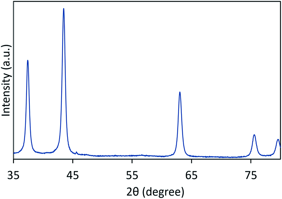 | ||
| Fig. 2 The XRD pattern of NiO nanoparticles. | ||
When subjected to FTIR scanning at wavelength range of 450–3500 cm−1 at room temperature, a broad absorption peak at ∼3320 cm−1 can be seen in Fig. 3, which arises due to O–H stretching and the bending vibration of the intercalated free water molecules from to absorbed moisture.39 Absorption peaks centered at ∼2935 and ∼2812 cm−1 correspond to the C–H stretching due to the vibration of –CH3 and –CH2 groups in chitosan polymer.40 Absorption peaks near 1555, 1407, and 1027 cm−1 that ascribed to symmetric bending of NH2, C–N, and C–O groups present in chitosan40–42 can also be observed in the figure. The presence of NiO nanoparticles in the thin film is validated by the presence of two absorption peaks at 745 and 602 cm−1 which are assigned to the stretching vibrations of the Ni–O bonds.43,44
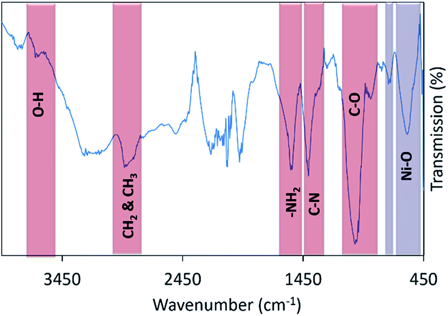 | ||
| Fig. 3 FTIR spectrum of NiO/chitosan film. | ||
The surface morphology of the NiO nanoparticles and elemental composition of the NiO/chitosan thin film are characterized using FESEM and EDX respectively with their results given in Fig. 3. As seen in Fig. 4(a), the FESEM image of the NiO nanoparticles at 130k magnification clearly shows a high yield of spherical nanoparticles with an average diameter of less than 25 nm. Meanwhile, the presence of NiO nanoparticles and chitosan in the thin film is confirmed by element mapping, as shown in Fig. 4(b). Four main elements are observed, with the presence of carbon (C) and nitrogen (N) corresponding to the chitosan film while the nickel (Ni) and oxygen (O) elements correlate to the NiO nanoparticles.45,46 All the elements are well-defined with sharp contrasts. Further analysis carried out by EDX confirms that the nanohybrid comprises of the C, O, N, and Ni elements, as given in Fig. 4(c). A Ni and O ratio of about 1.05![[thin space (1/6-em)]](https://www.rsc.org/images/entities/char_2009.gif) :0.95 observed from the spectrum is consistent with the theoretical value of NiO, while the presence of no other peaks in the spectrum indicates the purity of the fabricated NiO/chitosan film.
:0.95 observed from the spectrum is consistent with the theoretical value of NiO, while the presence of no other peaks in the spectrum indicates the purity of the fabricated NiO/chitosan film.
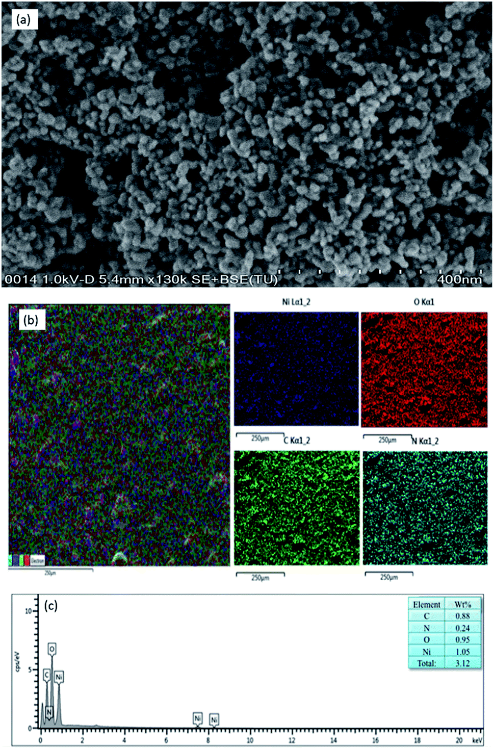 | ||
| Fig. 4 (a) FESEM image of the NiO nanoparticles drop-casted on the ITO substrate, (b) EDX mapping of Ni, O, C, and N elements, and (c) EDX analysis data of the plotted area. | ||
The size of the nanoparticles are not small enough to adversely affect the saturable absorption characteristics of the SA, leading to relatively typical SA behaviour.47 This was also demonstrated by Molli et al.,48 who showed similar behaviour in vanadium pentoxide (V2O5) nanoparticles.
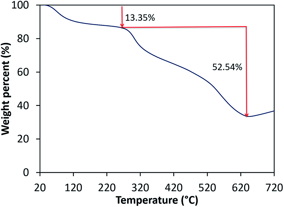
The thermal stability of the prepared films is studied using a TGA4000 Perkin Elmer Pyris Diamond Thermogravimetric Analyzer. The results are recorded between temperature range of 30 to 900 °C under N2 atmosphere at a heating rate of 10 °C min−1. The thermal stability of the NiO/chitosan film is depicted in Fig. 5, and from the TGA curves of the NiO/chitosan film, two thermal transitions at 28–259 °C and 259–629 °C can be observed. The initial weight loss of about 13.35% is observed within the temperature range of 28–259 °C due to the removal of absorbed water and hydroxide molecules from the prepared film49 and also indicates the formation of stable NiO nanoparticles.50 The final thermal transitions occur within the temperature range of 259–629 °C with a weight reduction of about 52.54% might cause by the degradation of polysaccharide and decomposition of chitosan molecules.51 The weight loss reaches a plateau when the temperature is higher than 630 °C with a remaining weight of about 34.11%. The total weight loss of the prepared films is found to be less as compared to other reports on chitosan,52 thus suggesting good thermal stability of the NiO/chitosan film.
 | ||
| Fig. 5 The TGA plot of the prepared NiO/chitosan film. | ||
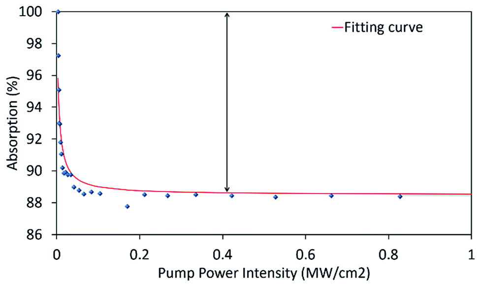
The twin-detector measurement technique is used to measure the nonlinear absorption characteristics of the NiO/chitosan thin film. A mode-locked laser is used to generate a seed signal at a lasing wavelength of 1560 nm with a pulse width of 0.71 ps and repetition rate of 28.17 kHz. The experimental data obtained, together with a fitted curve computed from the saturation model equation53 is given in Fig. 6. Based on the figure, the effective modulation depth, non-saturable losses, and saturation intensity of the NiO/chitosan thin film are calculated to be ∼11.50%, 88.50%, and 4.34 kW cm−2, respectively. The measured modulation depth the NiO/chitosan thin film is comparable to that of other materials such as WS2/PVA at 2%,54 Fe3O4/PVA at 1.80%,55 and gold nanorods/PVA at 4.06%.56 These results indicated that the NiO/chitosan film has a significant potential for use as SA.
 | ||
| Fig. 6 The measured nonlinear absorption of the prepared NiO/chitosan SA. | ||
Q-switched optical fiber laser set-up
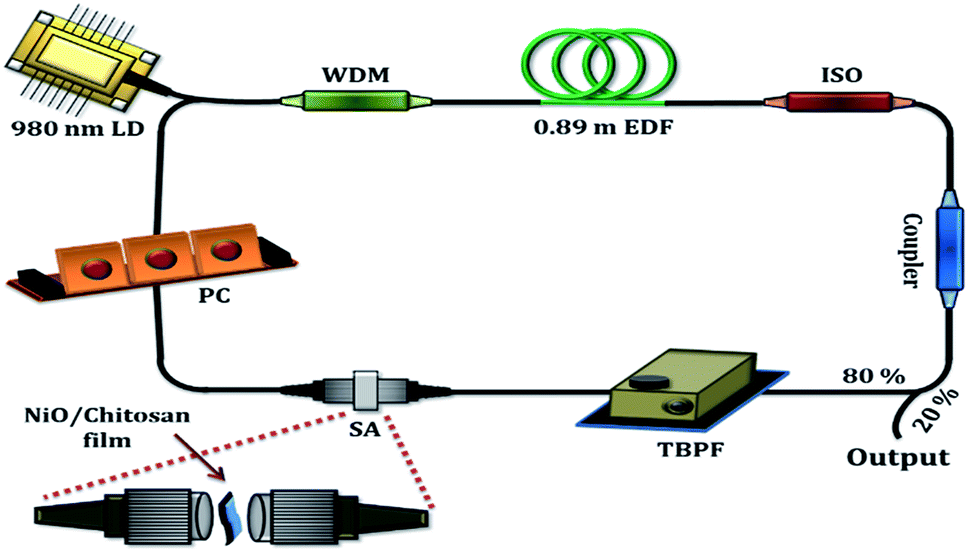
Fig. 7 shows the experimental set-up of the proposed tunable passively Q-switched EDFL with the NiO/chitosan thin film-based SA. A 980 nm laser diode (LD) acts as the pump sources and is connected to the 980 nm port of a 980/1550 nm wavelength division multiplexer (WDM). The common port of the WDM is now connected to a 0.89 m long erbium doped fiber (EDF) and is in turn connected to an isolator to ensure the unidirectional propagation of light in the cavity. The output of the isolator is connected to a fiber-based 80:20 optical coupler, which is used to extract approximately 20% of the propagating signal for analysis. The 80% port of the coupler on the other hand is connected to a tunable band pass filter (TBPF) with a tuning range up to 80 nm, and subsequently to the SA and a polarization controller (PC). Finally, the PC is connected to the 1550 nm port of the WDM, thus completing the optical circuit. The laser cavity has a total length of approximately 9.1 m with its insertion loss measured to be 3.66 dB. The 20% port of the optical circular is connected to another 50:50 optical coupler, with one end of the coupler connected to a Yokogawa AQ6370B optical spectrum analyzer (OSA) for optical spectrum and pulse shape measurements. The other end of the coupler is connected, in turn, to a Yokogawa DLM2054 mixed signal oscilloscope coupled with a photodetector, Anritsu MS2683 Radio-Frequency Spectrum Analyzer (RFSA) and a Thorlabs power meter for the measurement of the output in the frequency domain, as well as the measurement of the signal to noise ratio (SNR) and the output power of output pulses.
 | ||
| Fig. 7 Schematic illustration of the experimental set-up for the wavelength tunable passively Q-switched EDF laser cavity. | ||
Results and discussions
The CW lasing characteristics of the proposed laser are first determined by configuring the cavity in Fig. 7 with the omission of the SA. In this configuration, the lasing threshold of the proposed system under CW operation is determined to be 74.78 mW, giving a laser output with a power of 0.13 mW. Fig. 8 gives the optical spectrum of the CW signal taken from the system at a pump power of 171.30 mW. As can be seen from the figure, the CW output has a lasing wavelength with a narrow peak centred at 1567.35 nm, with a 3 dB bandwidth of 0.37 nm.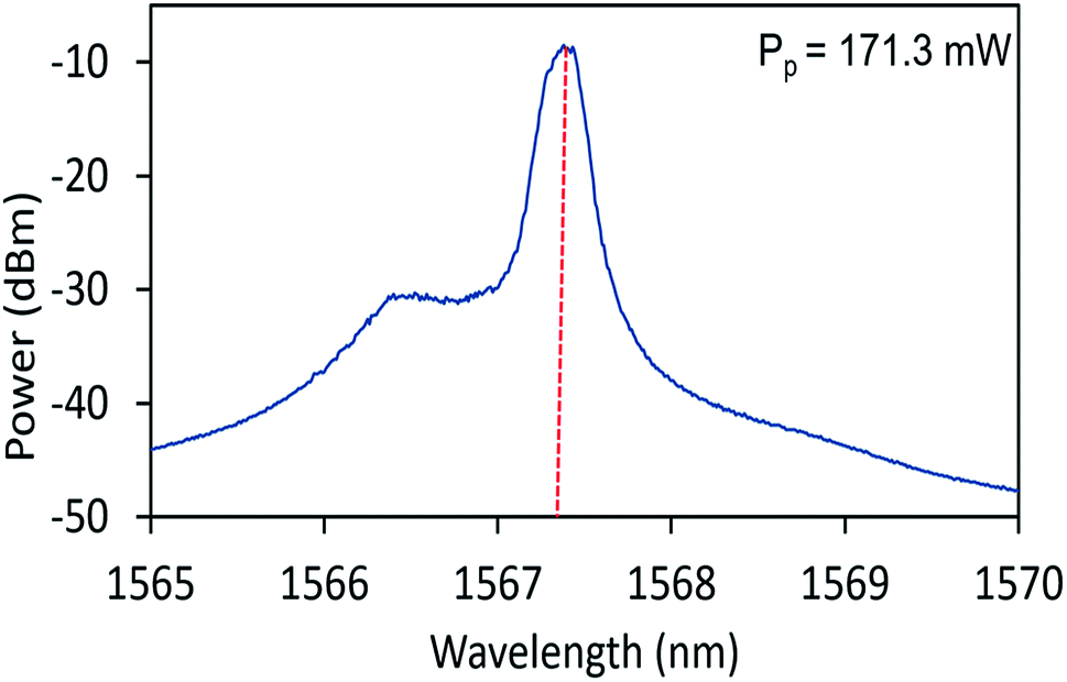 | ||
| Fig. 8 Optical spectrum of CW lasing output. | ||
Q-switched operation of the cavity is then achieved by integrating the NiO/chitosan based SA into the EDFL cavity, but without the TBPF present. Self-starting Q-switched operation at 1562 nm is observed at a threshold pump power of 104.90 mW with an average output power of 0.05 mW. It is observed that when the NiO/chitosan based SA is removed from the cavity, no pulsed outputs are observed, indicating that the SA is responsible for the generation of pulses and not any other optical phenomena. Fig. 9 gives the oscilloscope trace of the Q-switched pulses for three different pump powers. It can be seen that the pulse trains becomes narrower as the pump power is increased from 140.70 mW to 244.50 mW, along with the interval between pulses decreasing gradually as well. This is expected of the pulsed output and is a typical feature of passive Q-switching operation. It can also be seen that the Q-switched pulse train has uniform pulse shapes at different pump powers, indicating a high level of stability.
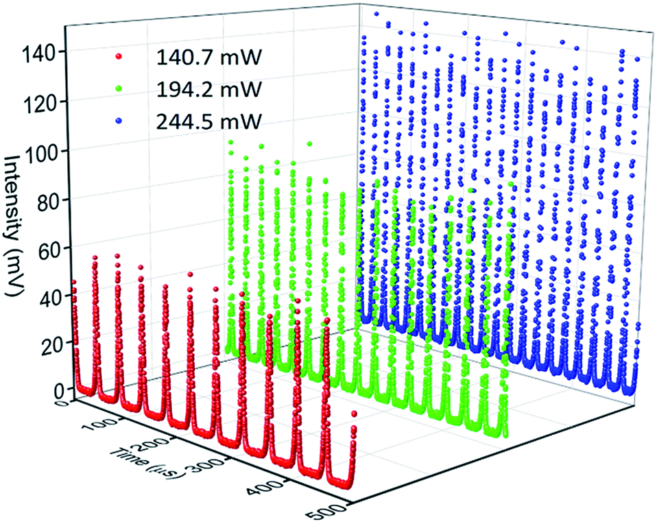 | ||
| Fig. 9 Q-switched pulse trains at pump powers of 140.7 mW, 194.2 mW and 244.5 mW. | ||
The typical output characteristics of the Q-switched laser at a pump power of 171.30 mW is given in Fig. 10. Fig. 10(a) shows the laser emission spectra with lasing observed at 1562 nm with a 3 dB bandwidth of 1.33 nm. It should also be noted that compared to CW lasing, the spectrum obtained under Q-switched lasing is broadened, with a shift to towards the low wavelength region. The broadening of the lasing spectrum is caused by the self-phase modulation (SPM) effect of the signal lasing in the cavity, as well as the shift of the system towards a higher gain region to compensate for losses induced by the insertion of the SA into the cavity.57 This provides additional validation that the NiO/chitosan based SA is responsible for inducing the Q-switched pulses in the cavity. As seen in Fig. 10(b), the laser cavity produces a stable pulse train with a repetition rate of 29.30 kHz and time interval between adjacent pulses of 34 μs. The focused view of the typical single pulse profile obtained under the afore-mentioned conditions is given in Fig. 10(c). It can be seen that the pulse envelope possess a symmetrical Gaussian-like shape with a full width at half maximum (FWHM) value of 2.90 μs, comparable to that reported works.58,59 From the radio frequency (RF) spectrum presented in Fig. 10(d), the SNR value is measured to be ∼43.26 dB at a fundamental frequency of 29.30 kHz, which demonstrates the good Q-switched stability. The measured SNR value is comparable to that obtained from similarly reported systems.60,61
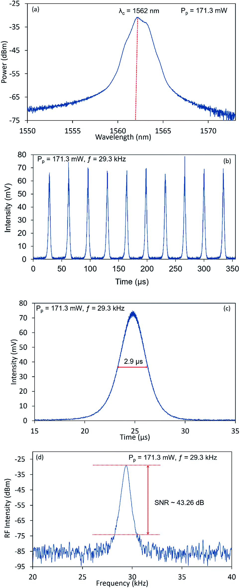 | ||
| Fig. 10 Typical characteristics of the Q-switched pulses generated from the EDF laser at a pump power of 171.30 mW, showing (a) the optical spectrum output, (b) the oscilloscope trace of the pulse train, (c) a single pulse profile and (d) the RF spectrum at fundamental frequency, fo = 29.30 kHz. | ||
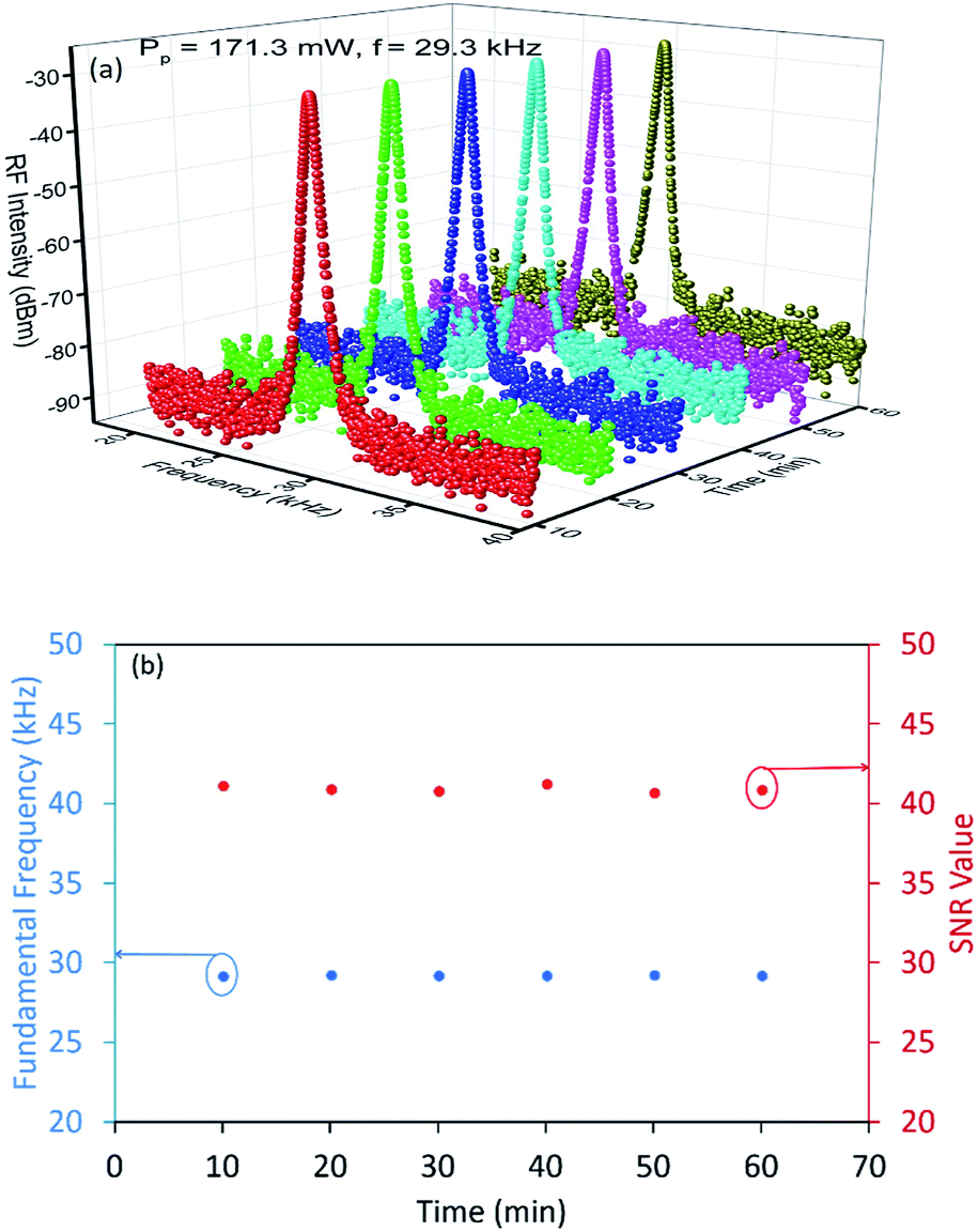
The stability of the laser system is observed by monitoring its power stability over a period of one hour. The RF spectra is recorded at intervals of every 10 minutes at a fixed pump power and repetition rates of 171.30 mW and 29.30 kHz, with the 3D plot of the RF spectra given in Fig. 11(a). No obvious changes are observed in the fundamental frequency and RF intensity during the test period, thus demonstrating that the generated pulses are highly stable. In addition to this, the trend of the SNR values as in Fig. 11(b), also indicates a highly stable pulsed output, with changes in the SNR value and fundamental frequency shows of less than 1 dBm and 0.10 kHz, respectively during the same observation period.
 | ||
| Fig. 11 (a) 3D plot of the RF spectra and (b) fundamental frequency and SNR value against time, recorded at 10 minutes intervals over a period of 1 hour. | ||
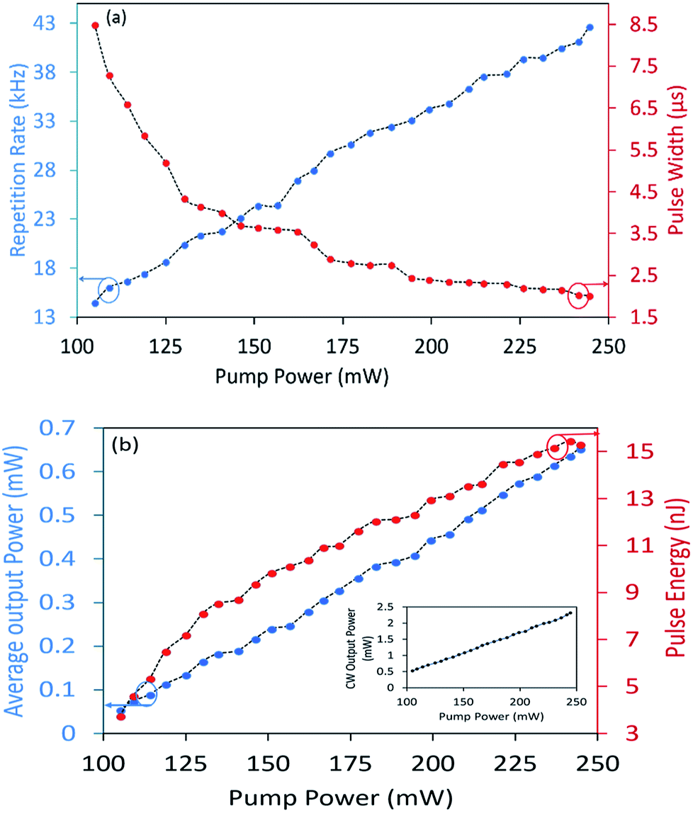
The response of the pulse duration and repetition rate of the Q-switched pulses against the pump power is given in Fig. 12(a). From the figure, it can be observed that the pulse duration and repetition rate increases linearly and decreases somewhat exponentially over a pump power range of 104.90 to 244.50 mW. The repetition rate at the minimum pump power is approximately 14.49 kHz, and increased to 42.66 kHz at the maximum pump power. The pulse width on the other hand is approximately 8.50 μs at the minimum pump power, and decreases exponentially until it reaches a value of 3.40 μs at a pump power of 194.20 mW, where it now decreases at a slower rate until reaching 2.02 μs at the maximum pump power.
 | ||
| Fig. 12 (a) Pulse width and repetition rate, and (b) pulse energy and average output power of the pulsed output against the pump power. Inset: The CW output power versus the pump power. | ||
Fig. 12(b) gives the response of the average output power and pulse energy against the rising pump power, and it can be seen from the figure that both the average output power and pulse energy grows linearly against the pump power, reaching its maximum values of 0.65 mW and 15.30 nJ at the maximum pump power. The dependence of the average output power of CW to the pump power is depicted in the inset of Fig. 12(b). From the figure, it can be seen that the average output power increases linearly with the incident pump power until a maximum output power of 2.32 mW is reached at a pump power of 244.50 mW. The slightly low laser slope efficiency is due to the insertion loss of the NiO/chitosan SA. The pulse energy obtained in this work is comparable to that reported in other Q-switched fiber lasers using graphene oxide62 and zinc oxide (ZnO).63 Moreover, the same trends can be observed should the pump power be reduced, indicating that the SA has not sustained any thermal damage and that its damage threshold is most likely higher than the maximum pump power available in this work.
At this point, the TBPF is introduced into the laser cavity to enable wavelength tunability of the proposed laser. The resulting tunability spectrum is given in Fig. 13, and shows a stable output over a wavelength range stretching from 1522 to 1580 nm. As shown in Fig. 13(a), a tuning range of 58 nm can be obtained covering the C and L bands as well as portions of the S band. The dependence of the repetition rate of the pulsed output at different tuning wavelengths is given in Fig. 13(b), and shows that the repetition rate increased from 16 kHz to 37.04 kHz when the wavelength is tuned from 1522 nm to 1530 nm. Increasing the lasing wavelength further results in the repetition rate decreasing to 5.38 kHz at a wavelength of 1580 nm. The observed trend of the repetition rate at different lasing wavelengths is observed to be very similar to that of the amplified spontaneous emission (ASE) spectrum of the EDF when pumped at 194.20 mW, as seen in the inset of Fig. 13(b). This is attributed to the fast population inversion from the strong intracavity laser at the larger gain region of the EDF, which in turn makes the bleaching process of the NiO/chitosan SA faster and thus resulting in a higher larger repetition rate.64 Furthermore, the dependency of the tunability on the bandwidth of the EDF gain medium shows no noticeable Q-switched pulses beyond the tunable wavelength range.
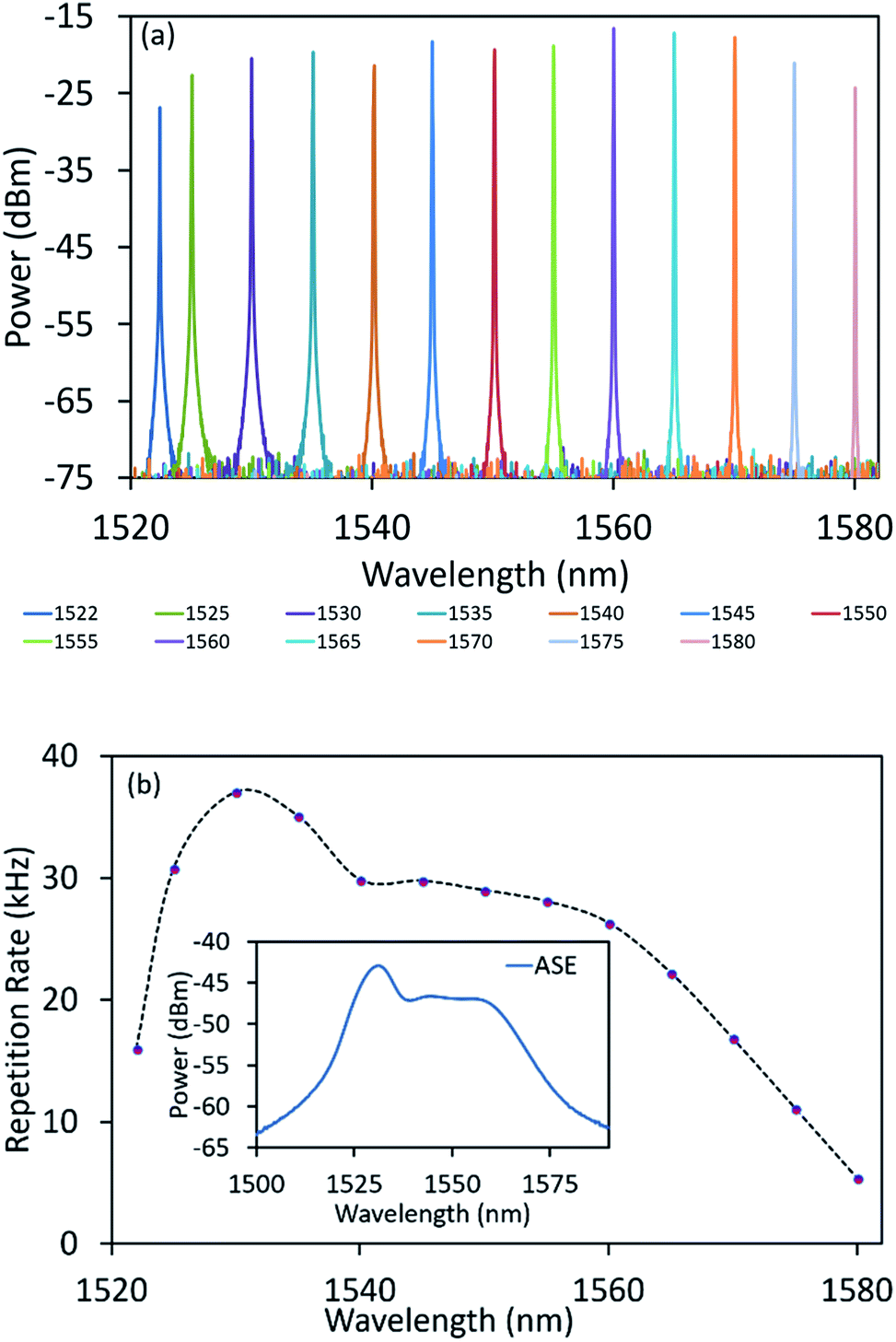 | ||
| Fig. 13 (a) The optical spectra of the Q-switching operation from 1522 nm to 1580 nm and (b) the repetition rate as a function of the tunable lasing wavelength. The inset of the figure shows the ASE spectrum of the EDF when pumped at 194.20 mW. | ||
Table 1 provides a comparison of the output performance parameters for the proposed Q-switched laser against similar designs utilizing various materials as SAs.
| SA | Operation wavelength (nm) | Tuning range (nm) | Repetition rate (kHz) | Min. pulse width (μs) | Max. pulse energy (nJ) | Ref. |
|---|---|---|---|---|---|---|
| a BP = Black phosphorus; GO = graphene oxide; ZnNPs = zinc nanoparticles; Fe2O4 = ferroferric oxide nanoparticles; PI = polyimide; CuNP = copper nanoparticles; MWCNT = multiwall carbon nanotubes; Ag = silver nanoparticles; MTMS = methyltrimethoxysilane; MoS2 = molybdenum disulfide; PVA = polyvinyl alcohol. | ||||||
| BP | 1562.35 | 9.61–44.72 | 9.80 | 81.50 | 65 | |
| GO | 1558.75 | — | 51.80–123.50 | 2.30 | 1.68 | 62 |
| ZnNPs | 1565.50 | — | 12.30–43 | — | 2.60 | 63 |
| Fe3O4/PVA | 1557 | — | 8.50–28 | 6 | 71 | 24 |
| Fe3O4/PI | 1562 | — | 5.50–49 | 3.50 | — | |
| CuNP/PVA | 1561 | — | 41.70–101.20 | 4.28 | 18.38 | 66 |
| MWCNT/PVA | 1519–1569 | 50 | 13.73–47.68 | 6.10 | 52.13 | 67 |
| Ag/MTMS | 1552.90–1580.20 | 27.30 | 10.50–24.40 | 6.54 | — | 68 |
| MoS2/PVA | 1519.60–1567.70 | 48.10 | 8.77–43.47 | 3.30 | 160 | 69 |
| NiO/Chitosan | 1522–1580 | 58 | 14.49–42.66 | 2.02 | 15.30 | This work |
It can be seen that the proposed system of this work is able to cover a wide C-band region as compared to other works. The tunability range of the proposed laser is also significantly better, as shown in Table 1. It is noted that while other works67,68 are able to be extended into the S-band region, similar to that of this work, the C-band region covered is not as broad. Furthermore, while other works successfully generate Q-switched pulses with a larger maximum pulse energy,24,65,67,69 the pulses produced in this work have the advantage of a shorter minimum pulse width. The system proposed by Mansoor et al.62 has a comparable minimum pulse width, though these pulses have a lower maximum pulse energy as compared that obtained in this work. As reported by T. Y. Tsai et al.,70 output pulses from Q-switched operations with a shorter pulse width is highly preferred for photonics applications. Thus, the proposed work has significant substantial potential for the generation of passively Q-switched pulses in the wideband C-band region for various photonics applications.
The maximum average output power can also be optimized by using a different optical coupler ratio, such as 90:10 or 95:5 to increase the power of the signal propagating in the cavity,71 and also by reducing the cavity length.72 Furthermore, the careful control of cavity losses73 as well as the use of fiber Bragg gratings to clamp the lasing wavelength74 can also boost the maximum average power output. Therefore, the proposed work with the generated pulses has substantial potential for the passively Q-switched pulses in the wideband C-band region especially in the photonics applications.
Conclusion
In this work, a broad range wavelength tunable passively Q-switched EDF laser with a NiO/chitosan thin film based SA is proposed and demonstrated. The proposed laser shows the feasibility of the NiO/chitosan thin film as an SA, and is capable of generating a tuning output over a range of 58 nm from 1522 to 1580 nm, covering the C and L bands and elements of the S band as well. A stable pulse train is obtained at a low threshold power of 104.90 mW at 1562 nm, with the highest pulse energy of 15.30 nJ and maximum repetition rate of 42.66 kHz obtained at the maximum pump power. A minimum pulse width of 2.02 μs is also obtained at this pump power. The output is highly stable, with an SNR of around 43 dB. The advantages of the chitosan film, which include its biocompatibility, non-toxicity and high thermal resistance make it a highly attractive candidate material for SA fabrication. The proposed SA will have many practical photonics applications, particularly for optical signal processing and optical fiber communication systems.Conflicts of interest
There are no conflicts to declare.Acknowledgements
This research was funded by the grant LRGS (2015) NGOD/UM/KPT from the Ministry of Higher Education, Malaysia and also the grants RU 001 – 2017 and RP 029B – 15 AFR from the University of Malaya. We would also like to acknowledge the Distinguished Visiting Fellowship for H. Ahmad from the Royal Academy of Engineering (UK) to City, University of London.References
- A. F. El-Sherif and T. A. King, Opt. Lett., 2003, 28, 22–24 CrossRef PubMed.
- C. Cuadrado-Laborde, A. Díez, J. L. Cruz and M. V. Andrés, Opt. Lett., 2009, 34, 2709–2711 CrossRef PubMed.
- Y. Lu and X. Gu, IEEE Photonics J., 2014, 6, 1–7 Search PubMed.
- Z. Yu, M. Malmström, O. Tarasenko, W. Margulis and F. Laurell, Opt. Express, 2010, 18, 11052–11057 CrossRef PubMed.
- J. Ren, S. Wang, Z. Cheng, H. Yu, H. Zhang, Y. Chen, L. Mei and P. Wang, Opt. Express, 2015, 23, 5607–5613 CrossRef PubMed.
- O. Buryy, A. Iznin, I. Syvorotka, D. Sugak, S. Ubizskii and M. Vakiv, Acta Phys. Pol., A, 2010, 117, 238–243 CrossRef.
- O. L. Antipov, N. G. Zakharov, M. Fedorov, N. M. Shakhova, N. N. Prodanets, L. B. Snopova, V. V. Sharkov and R. Sroka, Med Laser Appl, 2011, 26, 67–75 CrossRef.
- S. J. Ahn, J. H. Kim, D. W. Kim, H. S. Kim, Y. C. Kim, S. Ahn and C. Kim, Phys. Status Solidi B, 2004, 241, 1650–1653 CrossRef.
- T. S. Jang, S. S. Lee and Y. G. Kim, Ultrasonics, 2004, 42, 837–841 CrossRef PubMed.
- N. Trela, P. R. Kaczmarek and K. M. Abramski, Transparent Optical Networks, 2007. ICTON'07. 9th International Conference on IEEE, 2007, vol. 4, pp. 244–247 Search PubMed.
- S. R. Yemineni, A. Arokiaswami and P. Shum, Lasers and Electro-Optics Pacific Rim (CLEO-PR), 2017 Conference on IEEE, 2017, pp. 1–12 Search PubMed.
- B. Chen, X. Zhang, K. Wu, H. Wang, J. Wang and J. Chen, Opt. Express, 2015, 23, 26723–26737 CrossRef PubMed.
- Z. Luo, Y. Huang, J. Weng, H. Cheng, Z. Lin, B. Xu, Z. Cai and H. Xu, Opt. Express, 2013, 21, 29516–29522 CrossRef PubMed.
- D. Wu, Z. Cai, Y. Zhong, J. Peng, Y. Cheng, J. Weng, Z. Luo and H. Xu, IEEE J. Sel. Top. Quantum Electron., 2017, 23, 7–12 Search PubMed.
- M. F. M. Rusdi, A. A. Latiff, M. C. Paul, S. Das, A. Dhar, H. Ahmad and S. W. Harun, Opt. Laser Technol., 2017, 89, 16–20 CrossRef.
- Z. Qin, G. Xie, C. Zhao, S. Wen, P. Yuan and L. Qian, Opt. Lett., 2016, 41, 56–59 CrossRef PubMed.
- B. Xu, Y. Wang, J. Peng, Z. Luo, H. Xu, Z. Cai and J. Weng, Opt. Express, 2015, 23, 7674–7680 CrossRef PubMed.
- B. Xu, Y. Cheng, Y. Wang, Y. Huang, J. Peng, Z. Luo, H. Xu, Z. Cai, J. Weng and R. Moncorgé, Opt. Express, 2014, 22, 28934–28940 CrossRef PubMed.
- A. Nady, M. Ahmed, A. Numan, S. Ramesh, A. Latiff, C. Ooi, H. Arof and S. Harun, J. Mod. Opt., 2017, 64, 1315–1320 CrossRef.
- D. Mohammed, W. A. Khaleel and A. Al-Janabi, Opt. Laser Technol., 2017, 97, 106–110 CrossRef.
- A. Nady, A. Latiff, A. Numan, C. R. Ooi and S. Harun, Laser Phys., 2018, 28, 085106 CrossRef.
- B. Xuekun, M. Chengbo, X. Luxi, W. Shaofei, P. Shengli and Z. Xianglong, Appl. Phys. Express, 2016, 9, 042701 CrossRef.
- J. Guo, H. Zhang, C. Zhang, Z. Li, Y. Sheng, C. Li, X. Bao, B. Man, Y. Jiao and S. Jiang, Opt. Mater. Express, 2017, 7, 3494–3502 CrossRef.
- D. Mao, X. Cui, W. Zhang, M. Li, T. Feng, B. Du, H. Lu and J. Zhao, Photonics Res., 2017, 5, 52–56 CrossRef.
- H. Ahmad, A. S. Sharbirin, A. Muhamad, M. Z. Samion, S. A. Reduan, A. Z. Zulkifli and M. F. Ismail, J. Lightwave Technol., 2017, 35, 2470–2475 Search PubMed.
- N. Aziz, A. Latiff, M. Lokman, E. Hanafi and S. Harun, Chin. Phys. Lett., 2017, 34, 044202 CrossRef.
- H. Ahmad, C. S. J. Lee, M. A. Ismail, Z. A. Ali, S. A. Reduan, N. E. Ruslan, M. F. Ismail and S. W. Harun, Opt. Commun., 2016, 381, 72–76 CrossRef.
- A. Nady, M. H. M. Ahmed, A. A. Latiff, A. Numan, C. H. R. Ooi and S. W. Harun, Laser Phys., 2017, 27, 065105 CrossRef.
- M. Deshpande, K. N. Patel, V. P. Gujarati, K. Patel and S. Chaki, Adv. Mater. Res., 2016, 1141, 65 Search PubMed.
- H.-T. Wang, D. K. Mishra, P. Chen and J.-M. Ting, J. Alloys Compd., 2014, 584, 142–147 CrossRef.
- R. S. Kate, S. A. Khalate and R. J. Deokate, J. Alloys Compd., 2018, 734, 89–111 CrossRef.
- N. Duraisamy, A. Numan, S. O. Fatin, K. Ramesh and S. Ramesh, J. Colloid Interface Sci., 2016, 471, 136–144 CrossRef PubMed.
- D. Homa, Q. Zhang, C. Hill, G. Kaur and G. Pickrell, Curr. Appl. Phys., 2014, 14, 1396–1400 CrossRef.
- N. Sattarahmady, H. Heli and R. D. Vais, Biosens. Bioelectron., 2013, 48, 197–202 CrossRef PubMed.
- L. H. Chen, T. Li, C. C. Chan, R. Menon, P. Balamurali, M. Shaillender, B. Neu, X. M. Ang, P. Zu, W. C. Wong and K. C. Leong, Sens. Actuators, B, 2012, 169, 167–172 CrossRef.
- R. Raghunandhan, L. H. Chen, H. Y. Long, L. L. Leam, P. L. So, X. Ning and C. C. Chan, Sens. Actuators, B, 2016, 233, 31–38 CrossRef.
- S. Rakshit, S. Chall, S. S. Mati, A. Roychowdhury, S. Moulik and S. C. Bhattacharya, RSC Adv., 2013, 3, 6106–6116 RSC.
- B. Ingham and M. F. Toney, in Metallic Films for Electronic, Optical and Magnetic Applications, Woodhead Publishing, 2014, pp. 3–38, DOI:10.1533/9780857096296.1.3.
- M. El-Kemary, N. Nagy and I. El-Mehasseb, Mater. Sci. Semicond. Process., 2013, 16, 1747–1752 CrossRef.
- M. AbdElhady, Int. J. Carbohydr. Chem., 2012, 2012, 1–6 CrossRef.
- L. Vitali, K. C. Justi, M. Laranjeira and V. T. Fávere, Polimeros, 2006, 16, 116–122 Search PubMed.
- Y. Wang, A. Pitto-Barry, A. Habtemariam, I. Romero-Canelon, P. J. Sadler and N. P. Barry, Inorg. Chem. Front., 2016, 3, 1058–1064 RSC.
- P. Vijayadarshan, T. Mohan, J. V. Viswanath, K. Venugopal, N. S. Rao and A. Gupta, Mater. Sci. Res. India, 2017, 14, 37–42 CrossRef.
- T. Shahid, T. Khan, M. Zakria, R. Shakoor and M. Arfan, J. Mater. Sci. Eng., 2016, 5, 6 Search PubMed.
- J. Safari and L. Javadian, RSC Adv., 2014, 4, 48973–48979 RSC.
- Y. Chuminjak, S. Daothong, P. Reanpang, J. P. Mensing, D. Phokharatkul, J. Jakmunee, A. Wisitsoraat, A. Tuantranont and P. Singjai, RSC Adv., 2015, 5, 67795–67802 RSC.
- J. K. Anthony, H. C. Kim, H. W. Lee, S. K. Mahapatra, H. M. Lee, C. K. Kim, K. Kim, H. Lim and F. Rotermund, Opt. Express, 2008, 15, 11193–11202 CrossRef.
- M. Molli, G. D. Salian, S. K. Aditha, S. V. Muthukumar, T. M. Rattan, S. Amrithapandian, B. K. Panigrahi and V. Kamisetti, AIP Conf. Proc., 2012, 233–236 Search PubMed.
- A. Ashok, A. Kumar, R. R. Bhosale, M. A. H. Saleh and L. J. Van den Broeke, RSC Adv., 2015, 5, 28703–28712 RSC.
- T. Marimuthu, S. Mohamad and Y. Alias, Synth. Met., 2015, 207, 35–41 CrossRef.
- B. Lim, C. Poh, C. Voon and H. Salmah, Appl. Mech. Mater., 2015, 754–755, 34–38 Search PubMed.
- M. Karpuraranjith and S. Thambidurai, Int. J. Biol. Macromol., 2017, 104, 1753–1761 CrossRef PubMed.
- A. Martinez and S. Yamashita, in Carbon Nanotubes Applications on Electron Devices, InTech, 2011 Search PubMed.
- L. Li, Y. Wang, Z. F. Wang, X. Wang and G. Yang, Opt. Commun., 2018, 406, 80–84 CrossRef.
- J. Koo, J. Lee, J. Kim and J. H. Lee, J. Lumin., 2018, 195, 181–186 CrossRef.
- X.-D. Wang, Z.-C. Luo, H. Liu, N. Zhao, M. Liu, Y.-F. Zhu, J.-P. Xue, A.-P. Luo and W.-C. Xu, Opt. Commun., 2015, 346, 21–25 CrossRef.
- H. Ahmad, S. Ooi, Z. Tiu and B. Rahman, Opt. Commun., 2018, 426, 1–8 CrossRef.
- M. Zhang, G. Hu, G. Hu, R. C. T. Howe, L. Chen, Z. Zheng and T. Hasan, Sci. Rep., 2015, 5, 17482 CrossRef PubMed.
- Y. Chen, G. Jiang, S. Chen, Z. Guo, X. Yu, C. Zhao, H. Zhang, Q. Bao, S. Wen and D. Tang, Opt. Express, 2015, 23, 12823–12833 CrossRef PubMed.
- L. Baole, C. Haowei, J. Man, C. Xiaoming, R. Zhaoyu and B. Jintao, Laser Phys., 2013, 23, 045111 CrossRef.
- Y. Chen, C. Zhao, S. Chen, J. Du, P. Tang, G. Jiang, H. Zhang, S. Wen and D. Tang, IEEE J. Sel. Top. Quantum Electron., 2014, 20, 315–322 Search PubMed.
- A. Mansoor, B. A. Hamida, T. Eltaif, E. Ismail, N. Kadir, S. Khan and S. Harun, J. Opt. Commun., 2018, 307–310 Search PubMed.
- P. Zaca-Morán, J. G. Ortega-Mendoza, G. J. Lozano-Perera, L. C. Gómez-Pavón, G. F. Pérez-Sánchez, J. P. Padilla-Martínez and C. Felipe, Laser Phys., 2017, 27, 105101 CrossRef.
- Y. Huang, Z. Luo, Y. Li, M. Zhong, B. Xu, K. Che, H. Xu, Z. Cai, J. Peng and J. Weng, Opt. Express, 2014, 22, 25258–25266 CrossRef PubMed.
- N. N. Razak, A. A. Latiff, Z. Zakaria and S. W. Harun, Photonics Lett. Pol., 2017, 9, 72–74 CrossRef.
- A. Muhammad, M. Ahmad, R. Zakaria, H. Rahim, S. Yusoff, K. Hamdan, H. Yusof, H. Arof and S. Harun, Chin. Phys. Lett., 2017, 34, 034205 CrossRef.
- H. Ahmad, S. N. M. Hassan, F. Ahmad, M. Z. Zulkifli and S. W. Harun, Opt. Commun., 2016, 365, 54–60 CrossRef.
- H. Ahmad, N. E. Ruslan, Z. A. Ali, S. A. Reduan, C. S. J. Lee, R. A. Shaharuddin, N. Nayan and M. A. Ismail, Opt. Commun., 2016, 381, 85–90 CrossRef.
- Y. Huang, Z. Luo, Y. Li, M. Zhong, B. Xu, K. Che, H. Xu, Z. Cai, J. Peng and J. Weng, Opt. Express, 2014, 22, 25258–25266 CrossRef PubMed.
- T.-Y. Tsai and Y.-C. Fang, Opt. Express, 2009, 17, 1429–1434 CrossRef PubMed.
- W. Liu, X. Hu, L. Ying, S. Chen, J. Zhang, H. Akiyama, Z. Cai and B. Zhang, Sci. Rep., 2015, 5, 9600 CrossRef PubMed.
- N. A. M. A. Hambali, M. A. Mahdi, M. H. Al-Mansoori, M. I. Saripan and A. F. Abas, Appl. Opt., 2009, 48, 5055–5060 CrossRef PubMed.
- H. Ahmad, M. Z. Zulkifli, A. A. Latif and S. W. Harun, Opt. Commun., 2009, 24, 4771–4775 CrossRef.
- S. W. Harun, S. K. Low, P. Poopalan and H. Ahmad, IEEE Photonics Technol. Lett., 2002, 14, 293–295 Search PubMed.
Footnote |
| † Visiting Professor at the Department of Physics, Faculty of Science and Technology, Airlangga University, Surabaya 60115, Indonesia. |
| This journal is © The Royal Society of Chemistry 2018 |