
 Open Access Article
 This Open Access Article is licensed under a Creative Commons Attribution-Non Commercial 3.0 Unported Licence
Fabrication of nitrogen-doped ZnO nanorod arrays by hydrothermal synthesis and ambient annealing†
Ryosuke Kobayashi a,
Tetsuo Kishia,
Yuta Katayanagib,
Tetsuji Yanoa and
Nobuhiro Matsushita*a
a,
Tetsuo Kishia,
Yuta Katayanagib,
Tetsuji Yanoa and
Nobuhiro Matsushita*a
aDepartment of Materials Science and Engineering, School of Materials and Chemical Technology, Tokyo Institute of Technology, 2-12-1 Ookayama, Meguro-ku, Tokyo 152-8550, Japan. E-mail: matsushita.n.ab@m.titech.ac.jp; Fax: +81-3-5734-3353; Tel: +81-3-5734-2875
bDepartment of Technology Education, Faculty of Education, Gunma University, 4-2 Aramaki-machi, Maebashi, Gunma 371-8510, Japan
First published on 28th June 2018
Abstract
Nitrogen-doped ZnO nanorod arrays (N:ZnO NRAs) were fabricated by hydrothermal synthesis using a zinc–ammine complex solution, followed by annealing at elevated temperatures under ambient conditions. After annealing at 400 °C for 1 h, Raman spectra indicated that nitrogen was incorporated in the ZnO crystal structure. NH3-ligands in the zinc–ammine complex precursor were incorporated in ZnO crystals during hydrothermal crystal growth and were then ruptured during annealing. Photoluminescence spectra indicated that during post-annealing, the nitrogen was incorporated into the oxygen site, which created accompanying defects such as oxygen vacancies and/or interstitial oxygen. The absorption edge in diffuse-reflectance UV-visible spectra revealed visible absorption after post-annealing. In addition, the N:ZnO NRAs generated strong visible-light-induced photocurrents. Nitrogen doping caused a decline in carrier density, as confirmed by an electrochemical Mott–Schottky plot. These results suggest that this cost-effective fabrication has many potential applications such as solar-induced water splitting.
Introduction
Zinc oxide (ZnO) has many superior properties such as a wide, direct band gap, a large exciton binding energy, and high carrier mobility. Consequently, it has many applications.1–3 Moreover, one-dimensional ZnO nanostructures have high charge-carrier diffusion lengths, low grain boundaries, and a high surface-to-volume ratio, which are essential features for many optoelectronic applications.4–10 Photoelectrochemical water splitting under solar light has been explored extensively because of environmental issues.11,12In general, undoped ZnO is only active under ultraviolet light. To make it reactive to visible light, doping is a commonly used to modify its optoelectronic properties. In particular, nitrogen doping reduces the absorption energy and enables ZnO to absorb visible light.13 Hence, it is expected that nitrogen-doped ZnO nanorod arrays (N:ZnO NRAs) will be used for visible-light-reactive photoelectrodes.14
Typical N:ZnO NRAs fabrication involves dry processes, such as chemical vapor deposition15 and pulsed laser deposition,16 which require high-vacuum and high-temperature systems. Wet processes are much easier for fabricating undoped ZnO NRAs,17,18 and offer cost-efficiency and the potential for large-scale production. Generally, wet fabrication of N:ZnO NRAs requires two steps: a solution process, followed by post-doping via annealing in an ammonia gas atmosphere.14 Alternatively, ion implantation19 is used to incorporate nitrogen without changing the nanostructure. However, the dopant distribution within the crystal cannot be effectively controlled with annealing in ammonia gas,20,21 and complex, expensive systems are required for ion implantation.19 It is thus desirable to establish an easy, cost-effective method to fabricate uniformly nitrogen-doped N:ZnO NRAs.
Here, N:ZnO NRAs were fabricated by combining hydrothermal synthesis using a zinc–ammine complex solution, and post-annealing in an ambient atmosphere. The zinc–ammine complex solution was chosen as a precursor for the hydrothermal synthesis because it provided nitrogen sources via the NH3 ligands. The process was simple, and did not require specialized equipment or conditions. N:ZnO NRAs were obtained by annealing as-grown samples above 400 °C; visible light photocurrents were maximized when the sample was annealed at 500 °C. The nitrogen doping mechanism was as follows: (1) NH3 ligands in the zinc–ammine complex were incorporated in ZnO crystals during the hydrothermal crystal growth; (2) the ligands dissociated during annealing; and (3) nitrogen doping occurred within the ZnO crystals. Defect formation mechanisms followed by annealing were also investigated.
Experimental
Preparation of zinc–ammine complex solution
Zn(NO3)2·6H2O (>99%), NaOH (>97%), and NH3 aqueous solution (28%), all from Wako Pure Chemical Industries, Ltd., Japan, were used without further purification. A zinc–ammine complex precursor solution was prepared according to Meyers et al.22 Specifically, 10 ml of aqueous 2.5 M NaOH was added dropwise to 15 ml of aqueous 0.5 M Zn(NO3)2·6H2O under vigorous stirring. The resulting slurry was centrifuged and the supernatant was removed. Rinsing and centrifugation was performed four times to remove Na+ and NO3−. The precipitate was then dissolved in 50 ml of aqueous 6.6 M NH3 to yield the zinc–ammine complex solution.Preparation of ZnO seed layer
ZnO seed layers were deposited on a 20 mm × 30 mm FTO glass substrate (Sigma Aldrich, ∼7 Ω sq−1) by spin-coating the zinc–ammine complex solution. The substrate was first ultrasonically cleaned in acetone, then ethanol, and finally in distilled water for 10 min each. Then, the substrate was exposed to UV–ozone (ProCleaner™ Plus, Bioforce Nanosciences) for 10 min to produce a hydrophilic surface. The spin-coating was performed at 3000 rpm for 30 s. The substrate was then heated on a hot plate at 150 °C for 5 min. The spin-coating and heating steps were repeated ten times to get the desired ZnO thickness.Fabrication of N-doped ZnO nanorod arrays
The zinc–ammine complex solution was diluted by a factor of three with distilled water to form a growth solution. The substrate was placed in a Teflon vessel and 30 ml of the growth solution was added. The vessel was covered, tightly enclosed in a stainless autoclave, and placed in an oven. The hydrothermal reaction was performed at 100 °C for 24 h. The substrates were then removed and immediately rinsed with distilled water. Then the samples were dried in an oven at 100 °C for 10 min, and annealed at 300–700 °C with a programming rate of 10 °C min−1.Characterization
Crystal phases were determined by X-ray diffraction (XRD), (Bruker D8, Bruker), using Cu Kα radiation. Sample morphologies were imaged with field-emission scanning electron microscopy (FE-SEM) (S-4500, Hitachi). Diffuse reflectance spectra were recorded with a UV-vis spectrophotometer (V-670, JASCO), using BaSO4 as a reference material. Raman spectra were recorded with a Nanofinder30 spectrometer, using 532 nm excitation from a Nd:YAG laser. Photoluminescence (PL) spectra were recorded at room temperature with 325 nm excitation from a He-Cd laser. X-ray photoelectron spectroscopy (XPS) spectra were recorded on a Perkin-Elmer model 5500 MT XPS system, using monochromatic Al Kα radiation. Binding energies were calibrated with respect to the C 1s core level at 284.8 eV.Photoelectrochemical experiments
Photoelectrochemical characteristics were measured with a potentiostat (HZ-7000, Hokuto Denko), using a standard three-electrode cell under visible light irradiation from a 100 W xenon lamp equipped with a <422 nm cutoff filter (Asahi Spectra). N:ZnO NRAs on FTO substrates were used as working electrodes with an effective area of 4 cm2. A Pt plate and an Ag/AgCl electrode were used as counter and reference electrodes, respectively. A 0.1 M Na2SO4 aqueous solution was used as the electrolyte and was purged with Ar bubbling for 30 min before the experiments. Electrochemical impedance spectroscopy (EIS) was performed in a 0.5 M Na2SO4 electrolyte solution with a 5 mV amplitude, a 20 kHz to 1 Hz frequency range, and a potential range of −0.6 to 1.0 V vs. Ag/AgCl. Experimental setups are shown in Fig. S1.†Results and discussion
Fig. 1 shows the XRD patterns of as-grown N:ZnO NRAs and those annealed at 500 °C for 1 h. The peaks were identified as würtzite-type ZnO (JCPDS 36-1451), with no observed impurity phases. In particular, the (002) peak was the strongest, indicating preferential crystal orientation along the c-axis. This orientation has often been observed in solution-processed ZnO.17,18 Cross-sectional and top-view SEM images of the as-grown and annealed N:ZnO NRAs are also shown in Fig. 1. Nearly vertically aligned N:ZnO NRAs were obtained on the FTO substrate; their morphologies were maintained during annealing at 500 °C. The average diameter and length of the rods were approximately 210 nm and 12 μm, respectively.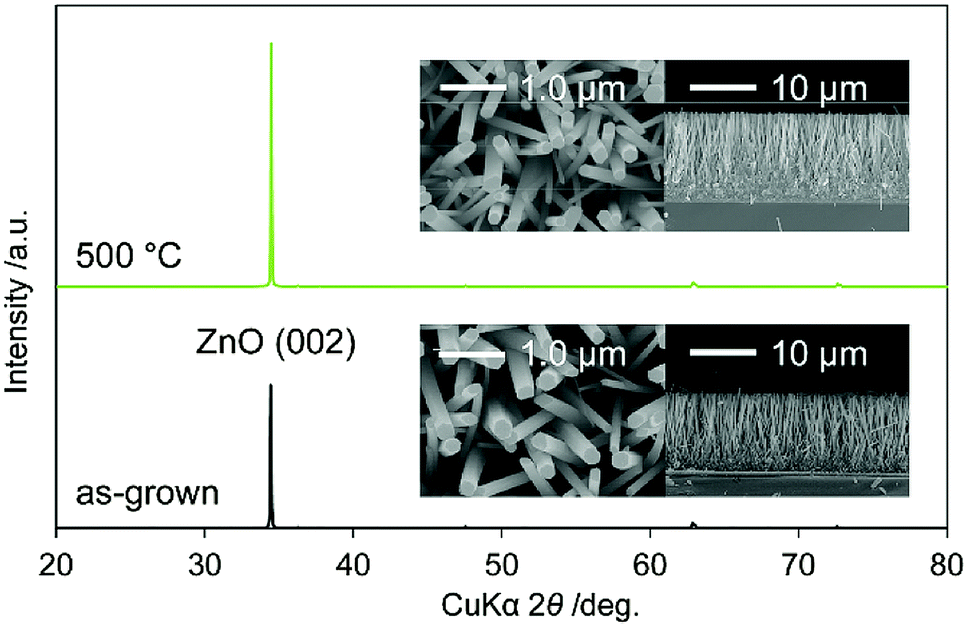 | ||
| Fig. 1 XRD patterns of as-grown N:ZnO NRAs and those annealed at 500 °C for 1 h. Cross-sectional and top-view SEM images are shown in the insets. | ||
Fig. 2 shows Raman spectra of the N:ZnO NRAs for the as-grown sample and for those annealed at different temperatures. All the spectra were normalized with respect to the highest peak intensity at 437 cm−1. This peak was observed for all samples, and was attributed to the characteristic vibration of the high-frequency E2 mode for würtzite-phase ZnO.23 Peaks at 330 cm−1 were from multiple phonon scattering E2 (MP).24
 | ||
| Fig. 2 Raman spectra of the as-grown N:ZnO NRA and those annealed at 300–700 °C for 1 h. All the spectra were normalized with respect to the peak intensity at 437 cm−1. | ||
Additional peaks at 275 cm−1, 510 cm−1, 582 cm−1, 635 cm−1 emerged after annealing above 400 °C; they are usually attributed to N-related local vibrational modes in ZnO.16,25–27 According to calculations by Friedrich et al.24 the peak at 275 cm−1 may be assigned to a vibrational mode between zinc interstitials (Zni) and the nitrogen substitution of oxygen (NO). It emerged after annealing above 400 °C, and thus indicated that nitrogen was incorporated into the oxygen site. The peak at 581 cm−1 was assigned to an A1 longitudinal optical peak derived from defects such as an oxygen vacancy (Vo), Zni, and defect complexes in ZnO.28,29 It disappeared after annealing at 300 °C, and appeared again after annealing above 400 °C. This result indicates that crystallinity was improved by annealing at 300 °C; whereas, new defects were created by nitrogen doping at annealing temperatures > 400 °C.
Fig. 3(a) shows the 275 cm−1 peaks in the Raman spectra fitted by Gaussian functions (dotted lines). Fig. 3(b) plots the calculated areas of the 275 cm−1 peaks vs. annealing temperature. The peak area increased with temperature, reached a maximum at around 500 °C, and then decreased above 600 °C. The peak intensity was a function of nitrogen dopant concentration.30,31 When annealing temperature < 400 °C, N–H bonds were not sufficiently broken; thus, N-related peaks were not observed. Temperatures above 400 °C were sufficient to rupture N–H bonding. The nitrogen remained in the crystal, while the hydrogen eventually diffused out.32
 | ||
| Fig. 3 (a) Raman spectra from Fig. 2 centered around 275 cm−1 and Gaussian fits. (b) Peak areas around 275 cm−1 vs. annealing temperature. | ||
To investigate sample defects, room-temperature PL spectroscopy was performed (Fig. 4). A strong near-band-edge luminescence at 380 nm is usually observed in ZnO,33 but was suppressed and very weak in all the samples. This suggested that the samples had many defects, decreasing band-to-band transitions, and increasing band-to-defect level transitions or defect level-to-band transitions. The origin of the broad visible luminescence has been controversial because of its complexity. Generally, the violet emission originates from Zni-to-valence band transitions,34 the yellow emission originates from OH groups made in the solution process,35 the orange emission originates from conduction band or Zni-to-oxygen interstitials (Oi),36 and the red emission originates from the conduction band-to-VO or VO-to-valence band transitions.37,38 Tarun et al. reported that the red emission originated from a nitrogen dopant state.39
 | ||
| Fig. 4 Photoluminescence spectra of N:ZnO NRAs after various annealing temperatures. | ||
In the as-grown sample, there were many OH group/VO defects remaining in the crystal, thus there was yellow/red emission in the spectra. Annealing at 300 °C reduced the number of OH groups/VO defects, decreasing the intensity of yellow/red luminescence. After 500 °C annealing, the Oi/VO defects increased because of N doping at oxygen sites, increasing the orange/red luminescence. Annealing at 700 °C reduced all the defects in the crystal, and the total luminescence decreased. These results were supported by the Raman spectra (Fig. 2), which revealed the existence of Zni, Oi, and VO defects. Differential scanning calorimetry (DSC) measurement of the sample also suggested the reduction of oxygen vacancies and the decomposition of the incorporated ammonia. More detailed thermal analysis is under investigation.
Diffuse reflectance absorption spectra of the N:ZnO NRAs are shown in Fig. 5. Before annealing, the absorption edge shifted to longer wavelengths relative to that reported for ZnO (∼380 nm). This red shift was due to VO defect levels created by NH3 ligand incorporation, consistent with Raman and photoluminescence spectra (Fig. 2 and 4). Similar absorption shifts induced by oxygen vacancies have been previously reported and applied in visible-light-reactive photocatalysts.40–42 After annealing at 300 °C, the absorption edge shifted to shorter wavelengths, similar to that previously reported for ZnO. Ambient annealing improved crystallinity and decreased the number of VO defects. Therefore, the absorption edge shift that had been caused by VO defects shifted back to the normal value for ZnO. After annealing at >400 °C, a broad shoulder absorption appeared around 500 nm that was attributed to the impurity levels formed by N doping.42 These changes in visible light absorption were consistent with color changes of the samples from pale-yellow (as-grown) to white (annealed at 300 °C) and to pale orange (annealed >500 °C), as shown in Fig. S2.†
 | ||
| Fig. 5 (a) Diffuse-reflectance UV-vis spectra of as-grown N:ZnO NRAs and those annealed at 300–700 °C for 1 h. (b) Enlarged spectra from (a). | ||
XPS spectra of the N 1s core levels for the samples are shown in Fig. 6. All the N 1s spectra exhibited single broad peaks, and they were deconvoluted into two peaks centered at 398.9 and 399.8 eV. The peaks around 398.9 eV were from nitrogen atoms in NH3,42,43 and the peaks around 399.8 eV were resulted from the formation of O–Zn–N bonds in the crystal.19,21,44 The intensity of O–Zn–N related peak increased after annealing at 500 °C. This result suggested that N was doped at the O sites in ZnO after 500 °C annealing, which strongly supports our discussion on nitrogen doping mechanism. Peak around 404 eV was not observed in the spectra. This peak has been assigned to (N2)O,45,46 thus the absence of the peak suggested the incorporated nitrogen was not from N2 molecule in the atmosphere, but from NH3 in the growth solution. The surface atomic ratio of N to Zn in the sample increased from 2.1% to 3.1% to 3.2% and to 4.7% in the as-grown sample and that annealed at 300 °C, 500 °C and 700 °C. This result suggests that nitrogen was incorporated inside the crystal during the crystal growth, and it thermally diffused from inside to the surface during the annealing.
 | ||
| Fig. 6 XPS spectrum of the N 1s region of as-grown N:ZnO NRAs and those annealed at 300–700 °C for 1 h. | ||
Fig. 7 shows photocurrent vs. time (I–t) measurements at 0.8 V recorded on N:ZnO NRAs with light on/off cycles using 422 nm illumination. The data show a very low dark current of <10−7 A cm−2. Upon illumination, an initial spike was observed in the photocurrent because of a power transient; the photocurrent then quickly relaxed to a steady-state value. The spikes were caused by photoexcited holes at electrode/electrolyte interfaces or at the interfaces within electrodes, which verified the existence of surface trap states in the sample.19 The maximum photocurrent occurred in the sample annealed at 500 °C. This was over 18 times that for the as-grown sample, which exhibited very low photocurrent. The relationship between photocurrent density and annealing temperature correlated with the 275 cm−1 Raman peak intensities.
 | ||
| Fig. 7 Electrochemical I–t measurements recorded on N:ZnO NRAs with light on/off cycles at 0.8 V using >422 nm illumination. | ||
To determine the carrier density and the flat-band potential of the N:ZnO NRAs, Mott–Schottky analysis was performed using EIS. For flat electrodes, the Mott–Schottky equation is expressed by:
 | (1) |
The impedance of the constant-phase element ZCPE was:
 | (2) |
In Fig. 8 is plotted C−2 vs. V. The positive slopes suggested that all the N:ZnO NRAs were n-type semiconductors, despite the nitrogen doping. There were two main reasons for n-type N:ZnO in this experiment. First, there were a lot of compensating donor defects in the sample. According to the Raman and PL spectra (Fig. 2 and 4), the existence of Zni and VO were suggested. These defects worked as electron donor and compensated the acceptor-nitrogen in the crystal. Second, the acceptor-nitrogen concentration was too low to turn n-type to p-type. The Raman peak intensities at 275 cm−1 (shown in Fig. 2) were weaker than those shown in the previous reports on p-type N:ZnO.21,27 This peak is assigned to a vibrational mode between Zni and NO, and thus it represents the amount of nitrogen in the crystal. The weak intensity of the peak insists low nitrogen concentration in the sample. To determine the apparent donor density ND from the Mott–Schottky analysis, the active surface area was estimated. N:ZnO NRAs were deposited on a 4 cm2 area, but the actual active surface area was much larger because of the side areas of the rod arrays. From the SEM image in Fig. 1, the actual surface area could be estimated from the rod lengths, diameters, and density. There were about 25 × 106 nanowires per cm2, with an average radius r = 210 nm and an average length h = 12 μm. Assuming a cylindrical surface area (Acylinder = 2πr2 + 2πrh), a total active surface area of A = 16.1 cm2 was determined.
 | ||
| Fig. 8 Mott–Schottky plots of N:ZnO NRAs under dark conditions as a function of various annealing temperatures (inset: equivalent circuit of the photoanode used for the calculations). | ||
The calculated donor densities and flat band potentials are listed in Table 1. A low carrier density was calculated for the as-grown sample because there were many defects revealed in the PL spectra. After annealing at 300 °C, the defect density was reduced and trapped electrons were released; thus, the donor density increased sharply. However, the donor density decreased after annealing above 500 °C, indicating that doped nitrogen acted as an accepter in the ZnO. The donor density continuously decreased up to 600 °C and then increased again with annealing at 700 °C. This implied that the nitrogen accepter diminished at higher temperatures. The flat band potential was negatively shifted after annealing at 300 °C, and then positively shifted after annealing at 500 °C. These results indicated that electrons were released and that the Fermi level rose after 300 °C annealing, and then the doped nitrogen and the Fermi level fell again after >500 °C annealing.
| Sample | Carrier density/cm−3 | Flat band potential/V vs. Ag/AgCl |
|---|---|---|
| As-grown | 4.76 × 10¹⁷ | 0.065 |
| 300 °C | 3.16 × 10²⁰ | −0.293 |
| 400 °C | 1.96 × 10¹⁹ | −0.218 |
| 500 °C | 7.00 × 10¹⁸ | −0.128 |
| 600 °C | 4.61 × 10¹⁸ | −0.041 |
| 700 °C | 6.55 × 10¹⁸ | −0.110 |
Conclusion
N:ZnO NRAs were fabricated by hydrothermal synthesis using a zinc–ammine complex solution, followed by post-annealing at various temperatures under ambient conditions. Raman and photoluminescence spectra indicated that post-annealing dissociated the NH3-ligands, allowing nitrogen to be incorporated at oxygen sites. When annealing occurred at a sufficiently high temperature, weak absorption appeared in the visible region (∼500 nm). The N:ZnO NRAs generated strong visible-light-induced (>422 nm) photocurrents after post-annealing. This procedure requires neither expensive nor complex equipment, and thus should be applicable for large-scale fabrication of N:ZnO NRAs.Conflicts of interest
There are no conflicts to declare.Acknowledgements
This work was supported by MEXT Nanotechnology platform 12025014(F-17-IT-0017) for the micro structure images of samples. A part of this work was financially supported by Research Grant, The Murata Science Foundation. We thank Alan Burns, PhD, from the Edanz Group (https://www.edanzediting.com/ac) for editing a draft of this manuscript.References
- S. Liang, H. Sheng, Y. Liu, Z. Huo, Y. Lu and H. Shen, J. Cryst. Growth, 2001, 225, 110–113 CrossRef.
- J. Xu, Q. Pan and Z. Tian, Sens. Actuators, B, 2000, 66, 277–279 CrossRef.
- X. Jiang, F. Wong, M. Fung and S. Lee, Appl. Phys. Lett., 2003, 83, 1875–1877 CrossRef.
- M. H. Huang, S. Mao, H. Feick, H. Yan, Y. Wu, H. Kind, E. Weber, R. Russo and P. Yang, Science, 2001, 292, 1897–1899 CrossRef PubMed.
- J. B. Baxter and E. S. Aydil, Appl. Phys. Lett., 2005, 86, 053114 CrossRef.
- X. M. Zhang, M. Y. Lu, Y. Zhang, L. J. Chen and Z. L. Wang, Adv. Mater., 2009, 21, 2767–2770 CrossRef.
- S.-J. Young, C.-C. Yang and L.-T. Lai, J. Electrochem. Soc., 2017, 164, B3013–B3028 CrossRef.
- C.-L. Hsu, Y.-H. Lin, L.-K. Wang, T.-J. Hsueh, S.-P. Chang and S.-J. Chang, ACS Appl. Mater. Interfaces, 2017, 9, 14935–14944 CrossRef PubMed.
- T. Chen, S. Young, S. Chang, C. Hsiao and C. Huang, J. Electrochem. Soc., 2012, 159, J153–J157 CrossRef.
- L.-W. Ji, C.-Z. Wu, C.-M. Lin, T.-H. Meen, K.-T. Lam, S.-M. Peng, S.-J. Young and C.-H. Liu, Jpn. J. Appl. Phys., 2010, 49, 052201 CrossRef.
- A. Wolcott, W. A. Smith, T. R. Kuykendall, Y. Zhao and J. Z. Zhang, Adv. Funct. Mater., 2009, 19, 1849–1856 CrossRef.
- H. M. Chen, C. K. Chen, Y. C. Chang, C. W. Tsai, R. S. Liu, S. F. Hu, W. S. Chang and K. H. Chen, Angew. Chem., 2010, 122, 6102–6105 CrossRef.
- D. Li and H. Haneda, J. Photochem. Photobiol., A, 2003, 155, 171–178 CrossRef.
- X. Yang, A. Wolcott, G. Wang, A. Sobo, R. C. Fitzmorris, F. Qian, J. Z. Zhang and Y. Li, Nano Lett., 2009, 9, 2331–2336 CrossRef PubMed.
- B. Xiang, P. Wang, X. Zhang, S. A. Dayeh, D. P. Aplin, C. Soci, D. Yu and D. Wang, Nano Lett., 2007, 7, 323–328 CrossRef PubMed.
- B. Yang, P. Feng, A. Kumar, R. Katiyar and M. Achermann, J. Phys. D: Appl. Phys., 2009, 42, 195402 CrossRef.
- M. Guo, P. Diao and S. Cai, J. Solid State Chem., 2005, 178, 1864–1873 CrossRef.
- A. Sugunan, H. C. Warad, M. Boman and J. Dutta, J. Sol-Gel Sci. Technol., 2006, 39, 49–56 CrossRef.
- M. Wang, F. Ren, J. Zhou, G. Cai, L. Cai, Y. Hu, D. Wang, Y. Liu, L. Guo and S. Shen, Sci. Rep., 2015, 5, 12925 CrossRef PubMed.
- R. G. Palgrave, D. J. Payne and R. G. Egdell, J. Mater. Chem., 2009, 19, 8418–8425 RSC.
- B. Chavillon, L. Cario, A. Renaud, F. Tessier, F. Cheviré, M. Boujtita, Y. Pellegrin, E. Blart, A. Smeigh and L. Hammarstrom, J. Am. Chem. Soc., 2011, 134, 464–470 CrossRef PubMed.
- S. Meyers, J. Anderson, C. Hung, J. Thompson, J. Wager and D. Keszler, J. Am. Chem. Soc., 2008, 130, 17603–17609 CrossRef PubMed.
- T. C. Damen, S. Porto and B. Tell, Phys. Rev., 1966, 142, 570 CrossRef.
- F. Friedrich, M. Gluba and N. Nickel, Appl. Phys. Lett., 2009, 95, 141903 CrossRef.
- A. Kaschner, U. Haboeck, M. Strassburg, M. Strassburg, G. Kaczmarczyk, A. Hoffmann, C. Thomsen, A. Zeuner, H. Alves and D. Hofmann, Appl. Phys. Lett., 2002, 80, 1909–1911 CrossRef.
- L. L. Kerr, X. Li, M. Canepa and A. J. Sommer, Thin Solid Films, 2007, 515, 5282–5286 CrossRef.
- N. P. Herring, L. S. Panchakarla and M. S. El-Shall, Langmuir, 2014, 30, 2230–2240 CrossRef PubMed.
- G. J. Exarhos and S. K. Sharma, Thin Solid Films, 1995, 270, 27–32 CrossRef.
- C. Youn, T. Jeong, M. Han and J. Kim, J. Cryst. Growth, 2004, 261, 526–532 CrossRef.
- J. Sann, J. Stehr, A. Hofstaetter, D. Hofmann, A. Neumann, M. Lerch, U. Haboeck, A. Hoffmann and C. Thomsen, Phys. Rev. B: Condens. Matter Mater. Phys., 2007, 76, 195203 CrossRef.
- K. Jindal, M. Tomar, R. Katiyar and V. Gupta, J. Appl. Phys., 2016, 120, 135305 CrossRef.
- J. Gao, X. Zhang, Y. Sun, Q. Zhao and D. Yu, Nanotechnology, 2010, 21, 245703 CrossRef PubMed.
- B. Meyer, H. Alves, D. Hofmann, W. Kriegseis, D. Forster, F. Bertram, J. Christen, A. Hoffmann, M. Straßburg and M. Dworzak, Phys. Status Solidi B, 2004, 241, 231–260 CrossRef.
- C. H. Ahn, Y. Y. Kim, D. C. Kim, S. K. Mohanta and H. K. Cho, J. Appl. Phys., 2009, 105, 013502 CrossRef.
- A. Djurišić, Y. Leung, K. Tam, Y. Hsu, L. Ding, W. Ge, Y. Zhong, K. Wong, W. Chan and H. Tam, Nanotechnology, 2007, 18, 095702 CrossRef.
- X. Liu, X. Wu, H. Cao and R. Chang, J. Appl. Phys., 2004, 95, 3141–3147 CrossRef.
- N. Alvi, K. Ul Hasan, O. Nur and M. Willander, Nanoscale Res. Lett., 2011, 6, 130 CrossRef PubMed.
- F. Stavale, L. Pascua, N. Nilius and H.-J. Freund, J. Phys. Chem. C, 2014, 118, 13693–13696 CrossRef.
- M. Tarun, M. Z. Iqbal and M. McCluskey, AIP Adv., 2011, 1, 022105 CrossRef.
- J. Wang, Z. Wang, B. Huang, Y. Ma, Y. Liu, X. Qin, X. Zhang and Y. Dai, ACS Appl. Mater. Interfaces, 2012, 4, 4024–4030 CrossRef PubMed.
- H.-L. Guo, Q. Zhu, X.-L. Wu, Y.-F. Jiang, X. Xie and A.-W. Xu, Nanoscale, 2015, 7, 7216–7223 RSC.
- X. Zong, C. Sun, H. Yu, Z. G. Chen, Z. Xing, D. Ye, G. Q. Lu, X. Li and L. Wang, J. Phys. Chem. C, 2013, 117, 4937–4942 CrossRef.
- X. Wang, J. C. Yu, Y. Chen, L. Wu and X. Fu, Environ. Sci. Technol., 2006, 40, 2369–2374 CrossRef PubMed.
- L.-C. Chen, Y.-J. Tu, Y.-S. Wang, R.-S. Kan and C.-M. Huang, J. Photochem. Photobiol., A, 2008, 199, 170–178 CrossRef.
- K. Ahn, Y. Yan, S. Lee, T. Deutsch, J. Turner, C. Tracy, C. Perkins and M. Al-Jassim, J. Electrochem. Soc., 2007, 154, B956–B959 CrossRef.
- C. Perkins, S. Lee, X. Li, S. Asher and T. Coutts, J. Appl. Phys., 2005, 97, 034907 CrossRef.
- I. Mora-Seró, F. Fabregat-Santiago, B. Denier, J. Bisquert, R. Tena-Zaera, J. Elias and C. Lévy-Clément, Appl. Phys. Lett., 2006, 89, 203117 CrossRef.
Footnote |
| † Electronic supplementary information (ESI) available. See DOI: 10.1039/c8ra04168g |
| This journal is © The Royal Society of Chemistry 2018 |