
 Open Access Article
 This Open Access Article is licensed under a Creative Commons Attribution-Non Commercial 3.0 Unported Licence
Synergetic photoluminescence enhancement of monolayer MoS2 via surface plasmon resonance and defect repair†
Yi Zenga,
Weibing Chenb,
Bin Tangac,
Jianhui Liao *a,
Jun Lou*b and
Qing Chen*ac
*a,
Jun Lou*b and
Qing Chen*ac
aKey Laboratory for the Physics and Chemistry of Nanodevices, Department of Electronics, Peking University, Beijing 100871, China. E-mail: jianhui.liao@pku.edu.cn
bDepartment of Materials Science and NanoEngineering, Rice University, Houston, Texas 77005, USA. E-mail: jlou@rice.edu
cAcademy for Advanced Interdisciplinary Studies, Peking University, Beijing 100871, China. E-mail: qingchen@pku.edu.cn
First published on 28th June 2018
Abstract
The weak light-absorption and low quantum yield (QY) in monolayer MoS2 are great challenges for the applications of this material in practical optoelectronic devices. Here, we report on a synergistic strategy to obtain highly enhanced photoluminescence (PL) of monolayer MoS2 by simultaneously improving the intensity of the electromagnetic field around MoS2 and the QY of MoS2. Self-assembled sub-monolayer Au nanoparticles underneath the monolayer MoS2 and bis(trifluoromethane)sulfonimide (TFSI) treatment to the MoS2 surface are used to boost the excitation field and the QY, respectively. An enhancement factor of the PL intensity as high as 280 is achieved. The enhancement mechanisms are analyzed by inspecting the contribution of the PL spectra from A excitons and A− trions under different conditions. Our study takes a further step to developing high-performance optoelectronic devices based on monolayer MoS2.
Introduction
Transition-metal dichalcogenides (TMDCs), such as MoS2, WS2, and MoSe2, have attracted much attention as two-dimensional (2D) semiconductors in recent years, due to their unique electrical and optical properties stemming from their atomic thicknesses.1–5 An intrinsic difference of monolayer TMDCs from graphene is the direct bandgap (such as the MoS2 monolayer with a bandgap of about 1.9 eV (ref. 6 and 7)), which enables these materials to have potential applications not only in field-effect transistors (FETs),8–11 but also in future optoelectronics (such as photodetectors and phototransistors).12–18 However, it is still a challenge to obtain high-performance optoelectronic devices made from monolayer TMDCs. Photoluminescence (PL) is one important technique in characterizing the optoelectronic properties of 2D semiconductors.6,7 Unfortunately, the PL intensity in pristine monolayer MoS2 is not high enough for realistic optoelectronic devices. Generally, the PL intensity mainly depends on the light-absorption and PL quantum yield (QY) in the materials. On one hand, the inherent atomic thickness of MoS2 monolayer leads to a very low light absorption, which is about 10% at the energy of A exciton and B exciton in the light absorption spectrum within the range from 1.3 eV to 2.4 eV.6 On the other hand, the defects (such as vacancies etc.) in MoS2 result in a low luminescence QY, which is at the level of 4 × 10⁻³ excited with a 532 nm laser.6,19 And the PL of MoS2 is a fluorescence process, considering the ultra fast PL decay time of MoS2, which was several nanoseconds as reported.20 Both the weak light absorption and low QY cause a weak PL intensity of MoS2. To obtain higher material performance, improving both the light absorption process and light emission process are vital. So far, many efforts have been made to improve the PL intensity of monolayer MoS2, including surface plasmon resonance (SPR) based on metallic nano-antennas,21–28 nanocavities,29 doping via chemical treatments,30–32 passivation engineering,20,33,34 and electrical tuning.35,36 Among these methods, the PL intensity of MoS2 monolayer was improved by either enhancing the excitation field21–28 or improving the QY.20,33,34 Note, compared to the effect of LSPR of Au NPs, the suspension effect on MoS2 on Au NPs could be negligible. As reported in previous work that weak enhancement was realized in the condition of MoS2 on Au NPs wrapped in thick HfO2 which maintained the morphology of Au NPs and have much weaker LSPR effect,28 also the results of suspended MoS2 on thick Al2O3/Au indicated that a suspension of MoS2 would not cause a high PL enhancement factor.22 Simultaneously improving both the excitation field and the QY of monolayer MoS2 has not been reported to the best of our knowledge. Here, we report a synergistic method to enhance the PL intensity of monolayer MoS2 by simultaneously utilizing both the SPR effect and the chemical treatment in order to repair defects. The uniform Au nanoparticles (NPs) arrays under the MoS2 monolayer can tremendously enhance the intensity of electromagnetic field around MoS2 (ref. 26, 28 and 37) and the defects effect can be ignored, considering the statistical results.28 Meanwhile, the bis(trifluoromethane)sulfonimide (TFSI) molecules passivated the sulfur vacancies in MoS2, which improved the QY in MoS2 prominently.20,34 Combining the advantages in both enhanced light intensity (light absorption process) and improved QY (light emission process), we realized the highest PL intensity enhancement factor of 280 and an average enhancement factor of 188 which were largely improved compared to the highest PL enhancement factor of 200 and average enhancement factor of 44 in our previous work.28 The prominent PL enhancement presented in this work provides a solid path to fabricate high-performance optoelectronic devices based on MoS2 and other 2D materials.Results and discussion
Fig. 1a shows schematically the structure of the samples measured in our experiments, in which a monolayer MoS2 triangle was put on a sub-monolayer Au NPs array and the surface of the MoS2 was treated by TFSI molecules. To construct this sample structure, we started from the self-assembly of sub-monolayer Au NPs. Au NPs with 10 nm diameter were immobilized from the water solution onto a SiO2/Si substrate by using (3-aminopropyl) triethoxysilane (APTES) molecules. From the absorption spectrum and finite difference time domain (FDTD) simulation of Au NPs (see ESI Fig. S1†), the resonance wavelength of the Au NPs with a diameter of 10 nm was about 520 nm, which is very close to 532 nm in our laboratory and the LSPR effect of Au NPs is satisfactory.28 We tuned the density of Au NPs to about 440 NPs/μm2 by transferring the Au NPs sub-monolayer onto a SiO2/Si substrate that was already decorated with Au NPs, using the method described in our previous paper.28 Monolayer MoS2 triangles were grown by chemical vapor deposition (CVD) on SiO2/Si substrates and confirmed by Raman, XPS, TEM and STEM.38 To minimize the effect of tensile strain, the CVD-grown MoS2 monolayer was first transferred onto another clean SiO2/Si substrate using the nondestructive poly(methylmethacrylate) (PMMA)-assisted wet transferring technique.34 Subsequently, the PL spectra of MoS2 on SiO2/Si substrate was measured. For comparison, the second PL measurement was conducted after transferring the same MoS2 monolayer onto a SiO2/Si substrate with a sub-monolayer of Au NPs. Then, we treated the MoS2 monolayer with TFSI molecules using the method as reported.20 Afterwards, we did a third PL measurement. The PL enhancement factors were systematically investigated by comparing the maximum intensity of PL spectra of these three measurements performed at the same experimental conditions. The same sample positions were selected in these three measurements to make reliable comparison. Also, to avoid the edge effect, the measured positions were not close to edges based on the large length of MoS2 triangles which is ∼60 μm and the small laser beam size which is about 1–2 μm.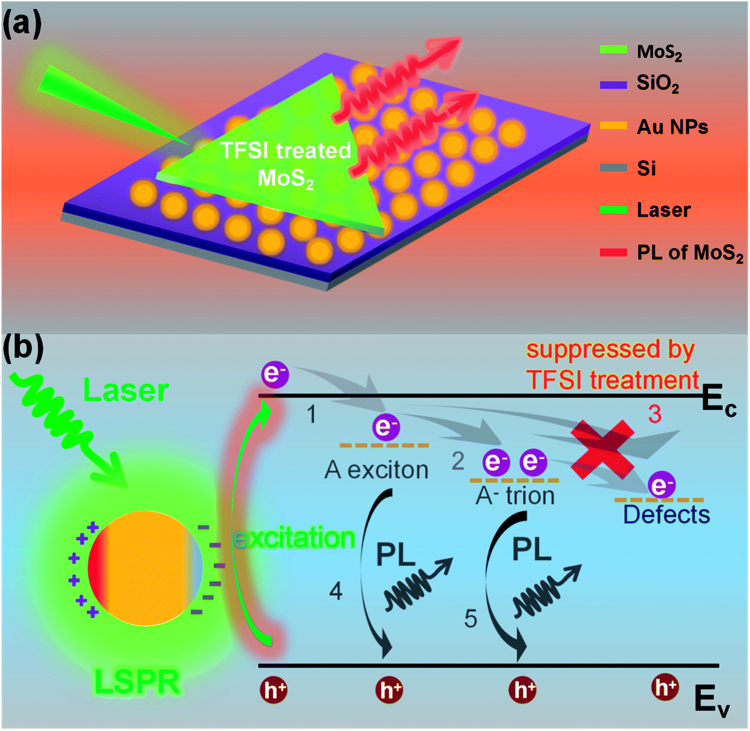 | ||
| Fig. 1 Schematic illustration of the sample structure and PL enhancement mechanism in this system. (a) Diagram of the sample structure of TFSI treated MoS2 on Au NPs. The MoS2 monolayer was transferred onto a SiO2/Si substrate with Au NPs and the MoS2 surface was subsequently treated with TFSI molecules. (b) The PL mechanism in this system. Under the laser illumination, electron-hole pairs are created. The LSPR of Au NPs will improve the light absorption in MoS2. The TFSI treatment will inhibit the nonradiative recombination (represented by red arrow 3). Excitons or trions decay through the radiation recombination (represented by gray arrows 4 and 5). | ||
Fig. 1b illustrates the PL process of a MoS2 monolayer and the enhancement mechanism used in this work. Normally, there are two sub-processes in the PL process of monolayer MoS2, i.e., the light-absorption and the light-emitting. During the light-absorption process, upon excitation of a 532 nm laser, some electrons in the valence band (Ev) of MoS2 will be excited into the conduction band (Ec), then relax into the excitonic or trionic level to form excitons or trions (represented by gray arrows 1 and 2).39 Although the light-matter interaction is strong in MoS2, the natural atomic thickness restricts the absorption,6,40 resulting in a limited population of excitons and trions. On the other hand, the process of emitting is seriously affected by the population of defects.20 The electrons in Ec, excitons and trion levels are partially trapped by the defects in MoS2, and decay through a nonradiative recombination (represented by the grey arrow 3). The remaining excitons and trions decay through a radiative recombination (represented by gray arrows 4 and 5).20,41,42 The PL energy of excitons is different from that of trions because of the different binding energy.35,43,44 Based on the analysis of the PL process, we propose a strategy to enhance the PL intensity through two processes, i.e., the light-absorption and the light-emitting. Firstly, upon the 532 nm laser excitation, which is a appropriate wavelength as reported in our previous work,28 the localized surface plasmon resonance (LSPR) of 10 nm Au NPs is excited (represented by the green halo around the Au NP) and the electromagnetic field around Au NPs is strengthened26,28 (see ESI Fig. S2†). Hence much more electrons are excited into the conduction band of MoS2, resulting from the interaction between the enhanced electromagnetic field and the monolayer. Therefore, the population of excitons and trions increases. Secondly, with the TFSI treatment, the defects in MoS2 are passivated and the nonradiative recombination rate is largely suppressed.20 Subsequently, more excitons or trions decay through a radiative recombination. Based on these two proposed improvements, we expect that the PL intensity of MoS2 could be strongly enhanced.
Before our experiments, we first inspected the quality of the MoS2 sample by using Raman spectroscopy. The differential between the E12g peak and the A1g peak is 20.4 cm−1, which confirms the monolayer nature of MoS2 (ref. 45) (see ESI Fig. S3†). To avoid other effects (such as thermal effect) on MoS2 during PL measurements, each spectrum was acquired in 2 s and a relatively low laser power of 3.9 μW of 532 nm excitation was selected. Fig. 2a shows an optical image of a TFSI treated MoS2 monolayer on Au NPs. The MoS2 crystal has a triangle shape with the side length of about 60 μm. Fig. 2a also confirms that the TFSI treatment does not affect the morphology of MoS2, which is consistent with the previous reports.20,33 The density of Au NPs of all our samples was about 440 NPs/μm2 (as shown in Fig. S4 in the ESI†), which is a proper density that could enhance the light-absorption in MoS2 as we previously reported.28
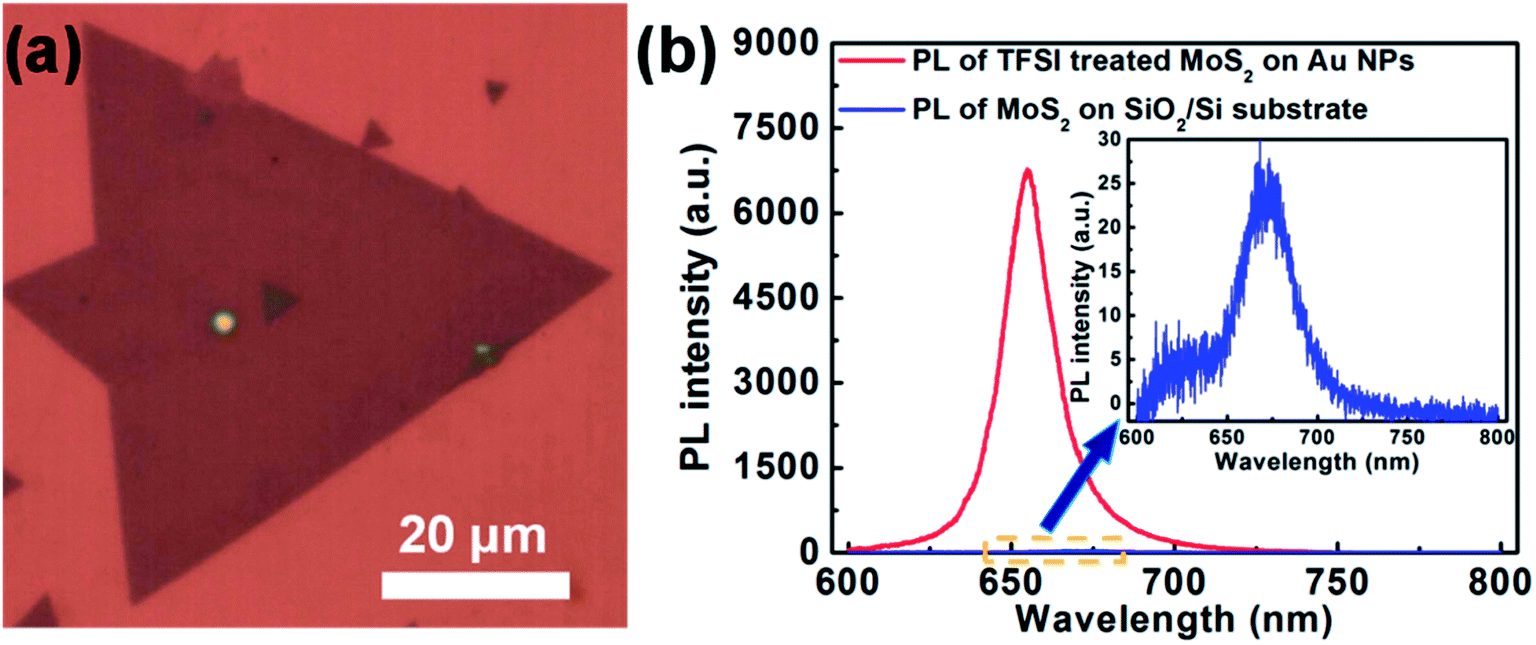 | ||
| Fig. 2 Optical image of the TFSI treated MoS2 monolayer on Au NPs and typical PL spectra. (a) Optical image of a MoS2 triangle transferred onto Au NPs and subsequently treated by TFSI molecules. (b) Typical PL spectra of MoS2 measured on the SiO2/Si substrate (blue curve) and on Au NPs after TFSI treated (red curve). Inset: The enlarged PL spectrum of MoS2 on the SiO2/Si substrate. | ||
Fig. 2b shows the PL spectra measured on the same position of a MoS2 sample on a SiO2/Si substrate and on Au NPs after TFSI treatment. The PL intensity was enlarged from 23.8 to 6693. This indicates a total enhancement factor of 280 by utilizing Au NPs plus the TFSI treatment. The inset in Fig. 2b shows the PL spectrum of the pristine MoS2 on the SiO2/Si substrate. There are two peaks (620 nm and 670 nm) in the PL spectrum, which come from the valence band splitting at K point in the Brillouin zone.6 Here we focus on the peak around 670 nm, which is contributed by the A excitons and A− trions.29,35
To evaluate the enhancement effect, we measured the PL intensities of monolayer MoS2 with only the presence of Au NPs, or TFSI, or both, respectively. For the same monolayer MoS2 sample, we measure the PL spectra of the same positions for the three situations, i.e., the pristine MoS2, MoS2 on Au NPs, and TFSI treated MoS2 on Au NPs. Fig. 3a shows the results of these measurements of 54 points in 5 samples. The PL intensities of the MoS2 on Au NPs is averagely enhanced by 28.3 times comparing with that of the pristine MoS2, due to the LSPR effect of Au NPs. Excited upon a 532 nm illumination, the LSPR of Au NPs enhanced the excitation field around MoS2. Therefore, more electrons were excited from valence band to conduction band and more excitons or trions formed,26,28,37 which lead to higher PL intensity. After the TFSI treatment, the PL intensity was further enhanced. The average enhancement factor reached 188 with respect to the PL intensity of the pristine MoS2. This might be attributed to the passivation of defects in the MoS2 by TFSI molecules, so that most excitons and trions in excited states decay through a radiative recombination way.20,34,47
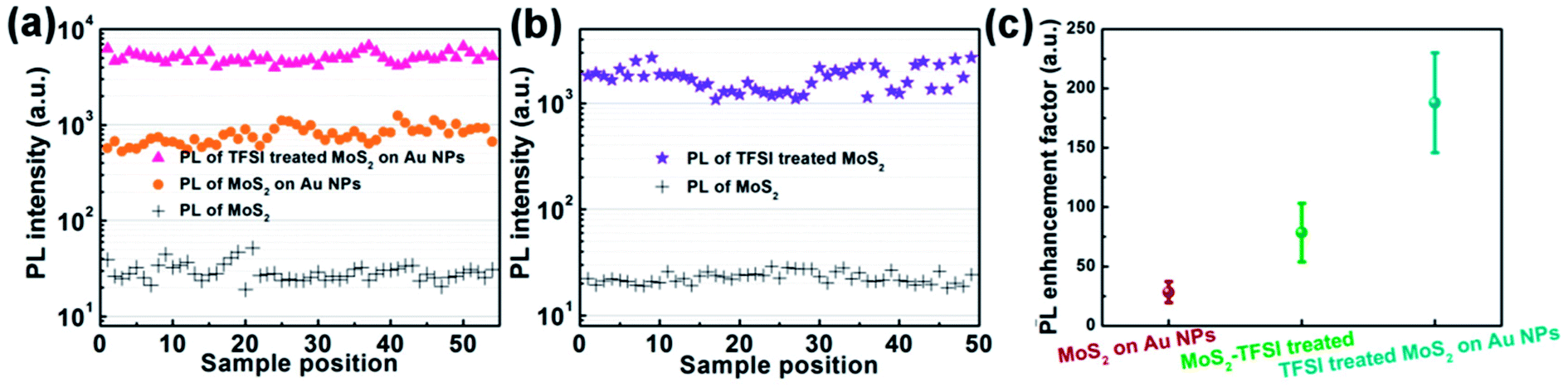 | ||
| Fig. 3 Statistics of PL intensity and enhancement factors of MoS2 under different circumstances. (a) Statistics of PL intensity of MoS2 on SiO2/Si substrate (black cross), on Au NPs (orange solid circle) and on Au NPs with TFSI treated (pink triangle). (b) Statistics of PL intensity of MoS2 on SiO2/Si substrate (black cross) and that after treated with TFSI (purple star). (c) PL enhancement factors in different conditions: MoS2 on Au NPs, MoS2 with TFSI treated, MoS2 on Au NPs with TFSI treated. | ||
To separately check the effect of the TFSI treatment without Au NPs, we measured another 5 samples on SiO2/Si substrate with 49 positions before and after the TFSI treatment, as shown in Fig. 3b. It shows that the PL intensities at all measured positions were remarkably enhanced after the TFSI treatment. The average enhancement factor is 78.4. Note that various PL enhancement factors due to the TFSI treatment ranging from 60 to 190 have been reported, which depends on the quality of the MoS2 monolayers.20,34,46 Nevertheless, our result indicates that the defects in MoS2 played an important role in the PL process. Even without the LSPR enhancement from Au NPs, the defects passivation in MoS2 monolayers could have a notable enhancement effect.
Fig. 3c shows the statistic results of the PL enhancement factors in the three conditions in this work. With respect to the PL intensity of the pristine MoS2, the average PL enhancement factors are 28.3, 78.4 and 188 for MoS2 on Au NPs, TFSI treated MoS2, and TFSI treated MoS2 on Au NPs, respectively. It is interesting to find that the PL enhancement factor for TFSI treated MoS2 on Au NPs was 188, which was much lower than multiplying the enhancement factor of MoS2 on Au NPs (28.3) by the enhancement factor of the TFSI treatment MoS2 (78). It might be attributed to the effect of the biexcitonic recombination, a two-body nonradiative process in TFSI treated MoS2 which occurs from the collision of two excitons, as reported in previous work.20,34,47 Generally, if the incident power is greater than 10−2 W cm−2, a high photon injection level in TFSI treated MoS2 occurs.47 The high populations of excitons leads to a high biexcitionic recombination, which results in a sublinear dependence of PL intensity with the incident power.20,33,34,47 In our experiments, the laser power was 3.9 μW and the spot diameter was about 1 μm. So, the power density was about 102 W cm−2, much larger than 10−2 W cm−2. Therefore, in our case, the PL intensity was in the sublinear region with respect to the incident power.47 The power-dependence of PL intensity in our experiments is consistent with previous work,20 as shown in Fig. S5.† Due to the limitation of our equipment, only 3 different power conditions are conducted. In this sublinear region, the QY of MoS2 decreases with increasing the incident power. The presence of Au NPs is to increase the electromagnetic intensity, i.e., the incident power. For the case of monolayer MoS2 on Au NPs, the incident power is increased by the Au NPs, resulting in the increase of the PL intensity though the QY is decreased. For the case of TFSI treated MoS2, only the QY is increased, leading to the increase of the PL intensity. However, when Au NPs and TFSI are simultaneously applied to the monolayer MoS2, there are two counterbalanced effects. On the one hand, the LSPR of Au NPs boosts the optical field and TFSI increases the QY. This tends to increase the PL intensity. On the other hand, the higher optical field due to the LSPR leads to a lower QY,47 since the incident power is in the sublinear region. This results in the decrease of the PL intensity. The overall enhancement factor is larger than that induced by Au NPs or TFSI treatment alone, which suggests that the enhancement effect dominates. But because of the counterbalanced effects, the PL enhancement factor of TFSI treated MoS2 on Au NPs was much lower than multiplying the enhancement factor of MoS2 on Au NPs by the enhancement factor of the TFSI treatment MoS2.
To further analyze the PL enhancement mechanism, we checked out the PL spectra closely. As we know, the PL spectrum of MoS2 originates from light emitting from A excitons, A− trions and B excitons.35 We fitted the PL spectra of MoS2 under different circumstances with three Lorentzian functions for A excitons (blue), A− trions (mignonette), B excitons (red),30,31 as shown in Fig. 4a. The black and pink curves are experiment and fitted data, respectively. The PL peak at the low wavelength (about 625 nm) is from B excitons, which originates from the splitting of valence band in MoS2. Normally, the PL of B excitons is very weak and we usually only consider the PL contributed by A excitons and A− trions for the case of MoS2 on Au NPs, TFSI treated MoS2 and TFSI treated MoS2 on Au NPs. (See ESI Fig. S6†). Based on the fitted curve, we did a statistic for the PL intensities of A excitons and A− trions, as shown in Fig. 4b. The average PL intensity of A exciton (23.1) is almost the same as A− trion (23.5) in the pristine MoS2. Though the overall PL intensity of MoS2 was enhanced, the relative PL intensities of the A excitons differs from that of A− trions in different situations. Meanwhile the peak position and Full Width at Half Maximum (FWHM) were distinct, as shown in Fig. S7.† Firstly, after being transferred onto Au NPs, the average PL intensity of A excitons and A− trions increased to 927 and 154, respectively. This kind of improvement was resulted from the enhanced electromagnetic field around MoS2 assisted by LSPR of Au NPs.26,28 More electrons in excited states would relax into excitonic and trionic levels. Consequently, the PL intensities of A excitons and A− trions are both enhanced. However, the difference (0.4 eV) in the Fermi energy between the MoS2 monolayer (4.7 eV)48,49 and Au (5.1 eV)50 is much lower than the energy of photons from 532 nm laser. Ref. 37 made a systematic research on MoS2–Au NPs hybrid. Upon 532 nm excitation, the electrons in excited state would transfer from MoS2 to Au, causing a p-doping in MoS2.37 Therefore, the population of trions reduced in comparison with that of excitons. Ultimately, the average PL intensity of excitons was higher than that of trions when MoS2 was transferred onto Au NPs.37 Secondly, the MoS2 monolayer treated by TFSI molecules increased the average PL intensity of A excitons and A− trions to 550 and 1962, respectively. Since the passivation suppressed the nonradiative recombination, an enhanced PL intensity of A excitons and A− trions was realized. The defects passivation caused a higher electron density and population of trions was greatly increased. Consequently, the PL intensity of A− trions is relatively stronger than A excitons, which is consistent with previous reports.41 Thirdly, in the case of TFSI treated MoS2 on Au NPs, the PL intensity of A excitons and A− trions increased to 5155 and 1793, which consequently contributes the highest PL intensity in MoS2 among the three conditions. These results show that both Au NPs and TFSI treatment can enhance the PL spectra of A excitons and A− trions, but their effects are different from each other. The Au NPs underneath MoS2 membrane can improve the intensity of electromagnetic field around MoS2 and enhance more light-emitting from A excitons than A− trion, while the TFSI treatment can improve the PL-QY of MoS2 and enhance more light-emitting from A− trions than A excitons.
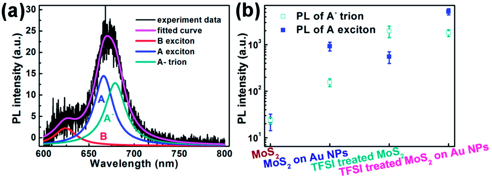 | ||
| Fig. 4 The PL spectra of A excitons and A− trions in MoS2. (a) The typical PL spectrum of MoS2 on SiO2/Si substrate (black curve). The pink line is the fitted curve to the experiment data with three Lorentzian functions for A excitons (blue), A− trions (mignonette), and B excitons (red). (b) Statistics on PL intensities of A excitons and A− trions in MoS2 under different circumstances. | ||
Conclusion
In summary, with the assistance of Au NPs and the TFSI treatment, a highly effective strategy to enhance the PL intensity of MoS2 is realized in this work. The LSPR of Au NPs under the 532 nm illumination enhances the electromagnetic field around MoS2, resulting a enhanced light-absorption in MoS2 and the defects passivation via the TFSI treatment can suppress the nonradiative recombination rate of excitons and trions. Combining the advantages of the two methods, the PL intensities of A excitons and A− trions were both enhanced. The effects of separate (Au NPs or TFSI treatment) and joint (Au NPs and TFSI treatment) enhancement factor on A excitons and A− trions were systematically investigated. The p-doping effect of Au induces a relative stronger PL intensity of A excitons and defects passivation of TFSI treatment causes a relative stronger PL intensity of A− trions. Our results provide an effective way to enhance the PL intensity of 2D materials. With the light-absorption and QY both improved, high-performance optoelectronic devices could be expected.Experimental section
CVD growth of monolayer MoS2
MoS2 monolayers were grown by high-temperature CVD with 80 sccm nitrogen as the protecting gas. A quartz tube with a diameter of 2 inches and a length of 135 cm was used with a crucible containing the precursor MoO3 powder (0.2 g) placed in the center. A silicon wafer with 300 nm thick SiO2 across this crucible was put upside down to catch the grown MoS2 monolayer. Another crucible containing sulfur powder (2 g) was put upstream at a distance of 25 cm away from the previous crucible. The furnace was heated from room temperature to 750 °C at the rate of 50 °C min−1 and kept for 10 min for the growth. The temperature of sulfur powder was estimated to 180 °C. After the growth, the furnace was cooled naturally. All the precursors were purchased from Sigma-Aldrich and used without any treatments.Preparation of Au NPs solution
Gold colloidal particles with a diameter of 10 nm were synthesized using the method described in the literature.51 Unless mentioned, all reagents were purchased from Sigma and used as received. A solution (20 mL) containing trisodium citrate (4 mL, 1% (w/v)) and tannic acid (0.08 mL, 1%) was rapidly added to a solution (80 mL) containing chloroauric acid (1 mL, 1% (w/v)) (all solutions at 60 °C). The mixed solution was boiled for 10 min with continuously stirring and then cooled to room temperature.Preparation of sub-monolayers of Au NPs
To prepare a sub-monolayer of Au NPs on the substrate, aminosilanes were used [i.e., APTES, Sigma-Aldrich, ≥98%] as molecular linkers. Firstly, a SiO2/Si substrate was cleaned in acetone, alcohol, and deionized water successively in an ultrasonic bath for 10 min in each solvent. After dried with nitrogen gas, the substrate was dealt with an oxygen plasma asher (PVA TePla Ion Wave 10, PDC-M) for 10 min at a power of 400 W to make the SiO2/Si substrate surface hydroxylated. Immediately afterward, the substrate was immersed in aqueous solution of APTES (3 × 10⁻³ M) for 45 min. The substrate was then rinsed in deionized water and dried with nitrogen gas. Afterward, it was placed in an oven (Memmert, UNB 100) at 120 °C for 30 min. The substrate was then immersed in the Au NPs aqueous solution for ≈1 h and rinsed in deionized water and dried with a nitrogen gas. Finally, to obtain a clean surface and eliminate the interference of APTES, the substrate was placed in an ozone asher (UVO cleaner 42-220) for 10 min to remove the APTES molecules, since UVO treatment is an effective method to remove a variety of contaminates from surface.52 A density of 440 NPs per μm2 of Au NPs was achieved by transferring a sub-monolayer of Au NPs onto a substrate already with a sub-monolayer of Au NPs.PMMA-assisted wet transferring technique
PMMA-assisted wet transferring technical was used to transfer samples from one substrate to another substrate in our experiments. To do this, a layer of PMMA (4% anisole solution, 950 kD) was spin-coated on MoS2 or Au NPs at a rate of 2000 rpm. Then, the substrate was placed in vacuum for 12 h at room temperature to solidify PMMA softly. The PMMA film with samples was suspended in solution after immersed in the buffered oxide etch (BOE, NH4F![[thin space (1/6-em)]](https://www.rsc.org/images/entities/char_2009.gif) :HF = 7:1, specification:UP grade) solution for 12 h. After cleaning it with deionized water for several times to remove residual BOE, the PMMA film was transferred onto the target substrate. After dried in ambient for 12 h, the substrate was placed on a heat plate at 100 °C for 3 min to make a close contact between the monolayer MoS2/Au NPs and the substrate. Finally, the PMMA was removed with acetone leaving MoS2/Au NPs on the SiO2/Si substrate.
:HF = 7:1, specification:UP grade) solution for 12 h. After cleaning it with deionized water for several times to remove residual BOE, the PMMA film was transferred onto the target substrate. After dried in ambient for 12 h, the substrate was placed on a heat plate at 100 °C for 3 min to make a close contact between the monolayer MoS2/Au NPs and the substrate. Finally, the PMMA was removed with acetone leaving MoS2/Au NPs on the SiO2/Si substrate.
TFSI treatment
20 mg bis(trifluoromethane)sulfonimide (TFSI) (Sigma-Aldrich) was dissolved in 10 ml 1,2-dichloroethane (DCE) (Sigma-Aldrich) to make a 2 mg mL−1 solution. The solution was further diluted with DCE to 0.2 mg mL−1. The samples (MoS2 on Au NPs substrates) were immersed in the TFSI solution at 100 °C for 10 min. Afterward, the samples were dried by nitrogen gas and put on a hotplate at 100 °C for 5 min.Optical measurements
The PL and Raman spectra were measured using a laser with 532 nm wavelength and 3.9 μW by the laserHoriba LabRAM ARAMIS-Raman spectrometer system (Jobin Yvon/Horiba company). The spectrometer for PL measurements was a grating of 600 gr mm−1. The Raman spectra were measured using a grating of 1800 gr mm−1 for high resolution. The objective lens with a magnification of 50 was utilized. The beam was focused to a spot with a diameter of about 1 μm. Each spectrum was acquired in 2 s.Conflicts of interest
There are no conflicts to declare.Acknowledgements
This work was financially supported by National Natural Science Foundation of China (No. 11528407 and 21573014) and the National Key Research & Development Program (Grant No. 2016YFA0201901 and 2016YFA0200802). Q. Chen and Y. Zeng were also supported by the National Natural Science Foundation of China (No. 61775006 and 61621061). J. Lou and W. Chen were also supported by the Welch Foundation Grant C-1716 and the AFOSR grant FA9550-14-1-0268. We also thank Prof. Yan Li and Dr Juan Yang for their assistance.References
- K. F. Mak and J. Shan, Photonics and optoelectronics of 2D semiconductor transition metal dichalcogenides, Nat. Photonics, 2016, 10(4), 216–226 CrossRef.
- L. Britnell, R. M. Ribeiro and A. Eckmann, et al., Strong light-matter interactions in heterostructures of atomically thin films, Science, 2013, 340(6138), 1311–1314 CrossRef PubMed.
- B. Radisavljevic, A. Radenovic and J. Brivio, et al., Single-layer MoS2 transistors, Nat. Nanotechnol., 2011, 6(3), 147–150 CrossRef PubMed.
- D. Lembke, S. Bertolazzi and A. Kis, Single-layer MoS2 electronics, Acc. Chem. Res., 2015, 48(1), 100–110 CrossRef PubMed.
- Z. Yin, H. Li and H. Li, et al., Single-layer MoS2 phototransistors, ACS Nano, 2011, 6(1), 74–80 CrossRef PubMed.
- K. F. Mak, C. Lee and J. Hone, et al., Atomically thin MoS2: a new direct-gap semiconductor, Phys. Rev. Lett., 2010, 105(13), 136805 CrossRef PubMed.
- A. Splendiani, L. Sun and Y. Zhang, et al., Emerging photoluminescence in monolayer MoS2, Nano Lett., 2010, 10(4), 1271–1275 CrossRef PubMed.
- D. Sarkar, X. Xie and W. Liu, et al., A subthermionic tunnel field-effect transistor with an atomically thin channel, Nature, 2015, 526(7571), 91–95 CrossRef PubMed.
- G. He, K. Ghosh and U. Singisetti, et al., Conduction mechanisms in CVD-grown monolayer MoS2 transistors: from variable-range hopping to velocity saturation, Nano Lett., 2015, 15(8), 5052–5058 CrossRef PubMed.
- H. Wang, L. Yu and Y. H. Lee, et al., Large-scale 2D electronics based on single-layer MoS2 grown by chemical vapor deposition, IEEE Int. Electron Devices Meet., 2012, 4.6.1–4.6.4 Search PubMed.
- A. B. Sachid, M. Tosun and S. B. Desai, et al., Monolithic 3D CMOS using layered semiconductors, Adv. Mater., 2016, 28(13), 2547–2554 CrossRef PubMed.
- D. Kufer and G. Konstantatos, Highly sensitive, encapsulated MoS2 photodetector with gate controllable gain and speed, Nano Lett., 2015, 15(11), 7307–7313 CrossRef PubMed.
- X. Wang, P. Wang and J. Wang, et al., Ultrasensitive and broadband MoS2 photodetector driven by ferroelectrics, Adv. Mater., 2015, 27(42), 6575–6581 CrossRef PubMed.
- Y. Xie, B. Zhang and S. Wang, et al., Ultrabroadband MoS2 Photodetector with Spectral Response from 445 to 2717 nm, Adv. Mater., 2017, 29(17), 1605972 CrossRef PubMed.
- Y. Li, J. G. DiStefano and A. A. Murthy, et al., Superior Plasmonic Photodetectors Based on Au@MoS2 Core–Shell Heterostructures, ACS Nano, 2017, 11(10), 10321–10329 CrossRef PubMed.
- X. Wan, K. Chen and Z. Chen, et al., Controlled Electrochemical Deposition of Large-Area MoS2 on Graphene for High-Responsivity Photodetectors, Adv. Funct. Mater., 2017, 27(19), 1603998 CrossRef.
- T. Y. Kim, J. Ha and K. Cho, et al., Transparent Large-Area MoS2 Phototransistors with Inkjet-Printed Components on Flexible Platforms, ACS Nano, 2017, 11(10), 10273–10280 CrossRef PubMed.
- J. H. Lee, H. Z. Gul and H. Kim, et al., Photocurrent Switching of Monolayer MoS2 Using a Metal–Insulator Transition, Nano Lett., 2017, 17(2), 673–678 CrossRef PubMed.
- H. Wang, C. Zhang and F. Rana, Ultrafast dynamics of defect-assisted electron–hole recombination in monolayer MoS2, Nano Lett., 2014, 15(1), 339–345 CrossRef PubMed.
- M. Amani, D. H. Lien and D. Kiriya, et al., Near-unity photoluminescence quantum yield in MoS2, Science, 2015, 350(6264), 1065–1068 CrossRef PubMed.
- B. Mukherjee, N. Kaushik and R. P. N. Tripathi, et al., Exciton Emission Intensity Modulation of Monolayer MoS2 via Au Plasmon Coupling, Sci. Rep., 2017, 7, 41175 CrossRef PubMed.
- Y. Yu, Z. Ji and S. Zu, et al., Ultrafast plasmonic hot electron transfer in Au nanoantenna/MoS2 heterostructures, Adv. Funct. Mater., 2016, 26(35), 6394–6401 CrossRef.
- W. Gao, Y. H. Lee and R. Jiang, et al., Localized and Continuous Tuning of Monolayer MoS2 Photoluminescence Using a Single Shape-Controlled Ag Nanoantenna, Adv. Mater., 2016, 28(4), 701–706 CrossRef PubMed.
- S. Butun, S. Tongay and K. Aydin, Enhanced light emission from large-area monolayer MoS2 using plasmonic nanodisc arrays, Nano Lett., 2015, 15(4), 2700–2704 CrossRef PubMed.
- S. Najmaei, A. Mlayah and A. Arbouet, et al., Plasmonic pumping of excitonic photoluminescence in hybrid MoS2–Au nanostructures, ACS Nano, 2014, 8(12), 12682–12689 CrossRef PubMed.
- A. Sobhani, A. Lauchner and S. Najmaei, et al., Enhancing the photocurrent and photoluminescence of single crystal monolayer MoS2 with resonant plasmonic nanoshells, Appl. Phys. Lett., 2014, 104(3), 031112 CrossRef.
- J. Li, Q. Ji and S. Chu, et al., Tuning the photo-response in monolayer MoS2 by plasmonic nano-antenna, Sci. Rep., 2016, 6, 23626 CrossRef PubMed.
- Y. Zeng, X. Li and W. Chen, et al., Highly Enhanced Photoluminescence of Monolayer MoS2 with Self-Assembled Au Nanoparticle Arrays, Adv. Mater. Interfaces, 2017, 4, 1700739 CrossRef.
- C. Janisch, H. Song and C. Zhou, et al., MoS2 monolayers on nanocavities: enhancement in light-matter interaction, 2D Materials, 2016, 3(2), 025017 CrossRef.
- S. Mouri, Y. Miyauchi and K. Matsuda, Tunable photoluminescence of monolayer MoS2 via chemical doping, Nano Lett., 2013, 13(12), 5944–5948 CrossRef PubMed.
- P. Hu, J. Ye and X. He, et al., Control of Radiative Exciton Recombination by Charge Transfer Induced Surface Dipoles in MoS2 and WS2 Monolayers, Sci. Rep., 2016, 6, 24105 CrossRef PubMed.
- W. Su, H. Dou and D. Huo, et al., Enhancing photoluminescence of trion in single-layer MoS2 using p-type aromatic molecules, Chem. Phys. Lett., 2015, 635, 40–44 CrossRef.
- H. Kim, D. H. Lien and M. Amani, et al., Highly Stable Near-Unity Photoluminescence Yield in Monolayer MoS2 by Fluoropolymer Encapsulation and Superacid Treatment, ACS Nano, 2017, 11(5), 5179–5185 CrossRef PubMed.
- M. Amani, R. A. Burke and X. Ji, et al., High luminescence efficiency in MoS2 grown by chemical vapor deposition, ACS Nano, 2016, 10(7), 6535–6541 CrossRef PubMed.
- K. F. Mak, K. He and C. Lee, et al., Tightly bound trions in monolayer MoS2, Nat. Mater., 2013, 12(3), 207–211 CrossRef PubMed.
- J. S. Ross, S. Wu, H. Yu, et al., Electrical Control of Two-Dimensional Neutral and Charged Excitons in a Monolayer Semiconductor, arXiv preprint arXiv:1211.0072, 2012.
- S. S. Singha, D. Nandi and A. Singha, Tuning the photoluminescence and ultrasensitive trace detection properties of few-layer MoS2 by decoration with gold nanoparticles, RSC Adv., 2015, 5(31), 24188–24193 RSC.
- S. Najmaei, Z. Liu and W. Zhou, et al., Vapour phase growth and grain boundary structure of molybdenum disulphide atomic layers, Nat. Mater., 2013, 12(8), 754–759 CrossRef PubMed.
- Z. Li, Y. Xiao and Y. Gong, et al., Active light control of the MoS2 monolayer exciton binding energy, ACS Nano, 2015, 9(10), 10158–10164 CrossRef PubMed.
- F. Xia, H. Wang and D. Xiao, et al., Two-dimensional material nanophotonics, Nat. Photonics, 2014, 8(12), 899–907 CrossRef.
- W. Su, H. Dou and D. Huo, et al., Enhancing photoluminescence of trion in single-layer MoS2 using p-type aromatic molecules, Chem. Phys. Lett., 2015, 635, 40–44 CrossRef.
- H. Shi, R. Yan and S. Bertolazzi, et al., Exciton dynamics in suspended monolayer and few-layer MoS2 2D crystals, ACS Nano, 2013, 7(2), 1072–1080 CrossRef PubMed.
- L. Wang, Z. Wang and H. Y. Wang, et al., Slow cooling and efficient extraction of C-exciton hot carriers in MoS2 monolayer, Nat. Commun., 2017, 8, 13906 CrossRef PubMed.
- H. S. Lee, M. S. Kim and H. Kim, et al., Identifying multiexcitons in MoS2 monolayers at room temperature, Phys. Rev. B, 2016, 93(14), 140409 CrossRef.
- W. Park, J. Baik and T. Y. Kim, et al., Photoelectron spectroscopic imaging and device applications of large-area patternable single-layer MoS2 synthesized by chemical vapor deposition, ACS Nano, 2014, 8(5), 4961–4968 CrossRef PubMed.
- F. Cadiz, S. Tricard and M. Gay, et al., Well separated trion and neutral excitons on superacid treated MoS2 monolayers, Appl. Phys. Lett., 2016, 108(25), 251106 CrossRef.
- M. Amani, P. Taheri and R. Addou, et al., Recombination kinetics and effects of superacid treatment in sulfur-and selenium-based transition metal dichalcogenides, Nano Lett., 2016, 16(4), 2786–2791 CrossRef PubMed.
- M. S. Choi, G. H. Lee and Y. J. Yu, et al., Controlled charge trapping by molybdenum disulphide and graphene in ultrathin heterostructured memory devices, Nat. Commun., 2013, 4, 1624 CrossRef PubMed.
- K. K. Liu, W. Zhang and Y. H. Lee, et al., Growth of large-area and highly crystalline MoS2 thin layers on insulating substrates, Nano Lett., 2012, 12(3), 1538–1544 CrossRef PubMed.
- H. B. Michaelson, The work function of the elements and its periodicity, J. Appl. Phys., 1977, 48(11), 4729–4733 CrossRef.
- J. Liao, L. Bernard and M. Langer, et al., Reversible formation of molecular junctions in 2D nanoparticle arrays, Adv. Mater., 2006, 18(18), 2444–2447 CrossRef.
- J. R. Vig, UV/ozone cleaning of surfaces, J. Vac. Sci. Technol., A, 1985, 3(3), 1027–1034 CrossRef.
Footnote |
| † Electronic supplementary information (ESI) available. See DOI: 10.1039/c8ra03779e |
| This journal is © The Royal Society of Chemistry 2018 |