
 Open Access Article
 This Open Access Article is licensed under a
 Creative Commons Attribution 3.0 Unported Licence
Quantum confined two-dimensional electron/hole gas switching by facet orientation of perovskite oxides†
Fei Zhouab,
Yong Liuad,
Zhonghong Laie,
Mingqing Liao a,
Yi Zhoua,
Yudong Huangb and
Jingchuan Zhu*acd
a,
Yi Zhoua,
Yudong Huangb and
Jingchuan Zhu*acd
aSchool of Materials Science and Engineering, Harbin Institute of Technology, 150001, Harbin, China. E-mail: fgms@hit.edu.cn
bMIIT Key Laboratory of Critical Materials Technology for New Energy Conversion and Storage, School of Chemistry and Chemical Engineering, Harbin Institute of Technology, 150001, Harbin, China
cNational Key Laboratory of Science and Technology on Advanced Composites in Special Environments, Harbin Institute of Technology, 150001, Harbin, China
dNational Key Laboratory for Precision Hot Processing of Metals, Harbin Institute of Technology, 150001, Harbin, China
eAnalysis and Testing Center, Harbin Institute of Technology, 150001, Harbin, China
First published on 5th June 2018
Abstract
The Polar discontinuity at heterointerface and the bare surface reconstructs the electronic phase of perovskite oxides. This gives rise to confined free electrons which intrinsically transit material from band insulator to metal. However, the insulator–metal transition induced by free holes has not been investigated so far due to the challenge in obtaining free hole state in oxides. Here, we propose a simple method whereby free holes can be obtained via polar facet reorientation. In the high polarity case, free holes can be supported by the lift up of O 2p subbands, which split into three independent subbands (one heavy hole subband and two light hole subbands) due to strong quantum confinement. Results show that both of the free electron and hole states are confined in a two dimensional quantum well, subjecting to the confined energy (E − EF) and occupied density of states around the Fermi level, indicating a finite thickness for preserving the metal states.
Introduction
Two-dimensional electron/hole gases (2DEGs/2DHGs) were first studied at the interfaces of semiconductor heterostructures.1,2 Recent studies have revealed the existence of high mobility 2DEGs at LaAlO3/SrTiO3 interface3 and even at the bare surface of SrTiO3,4,5 which are treated as the cornerstone of oxide electronics.6 Electronic reconstruction at interfaces or surfaces that occur to compensate for the polar discontinuity of adjacent constituents plays a key role in the formation of localized 2DEGs.7 This gives rise to attractive physics, such as insulating-metallic state transitions,8 superconductivity,9 spiral magnetism and giant negative magnetoresistance.10–12 These above-mentioned examples occur on n-type interface/surface, such as the interface construction of (LaO)+/(TiO2)0 or with defects created on bare SrTiO3 surface, leading to the mixed dimensionality of confined conducting electrons.13 On the contrary, it is still challenging to obtain the free holes at interfaces or surfaces of oxides,3,14 although recent experiment shows that strong hole carriers can be seen at the LaAlO3/SrTiO3 heterointerface by reducing the oxygen defects.15,16 However, 2DHGs have been researched in Ge/Si based semiconductor heterostructures, presenting novel physics, such as spin Hall effect induced edge-spin accumulation and well-controlled Coulomb blockade oscillations.17–19 The lack of investigations of 2DHGs on perovskite oxides might be ascribed to the limitation of current epitaxial growth technology, which generally allows films to grow along (001)cubic direction through substrate matching, preserving an extra e−/2 per unit cell on the discontinued interface or surface. Our recent experiments show that 2D potassium niobates can be grown automatically in liquid with facets of 60° tilting of oxygen octahedrons, providing a practical basis for the study of the facets effects to 2DEGs/2DHGs.In this letter, ab initio calculation is used to investigate the confined 2DEGs/2DHGs in 2D KNbO3. Results show that the increase of polar discontinuity by facets engineering would change the electronic phase of the material surface, leading to the formation of switchable 2DEGs and 2DHGs on 2D KNbO3 structures by varying facet orientations. These free electron/hole states around the Fermi level (EF) are strongly quantum localized. This concept not only endows the material with an insulator–metal transition, but also provide an opportunity for manipulating 2DEGs/2DHGs in the quantum confined regime.
Computational details
The first-principle calculation is performed with the Cambridge Serial Total Energy Package.20 2D crystal models are fully relaxed through geometry optimization according to system energy, force and stress by DFT with the Perdew, Burke, and Ernzerhof functional.21 For our main objective is qualitatively investigating the behaviors of quantum confined free electronic states, ultrasoft pseudopotentials are applied to describe the ionic cores with a plane-wave cutoff energy of 340 eV. The k-point sampling grids are 3 × 3 × 1 for 2D crystal slabs and 4 × 4 × 2 for bulk KNbO3 crystal, respectively. The vacuum spacing layer between neighboring repeat units of 2D slabs are set to 1 nm. The truncated surface are capped by H atoms, in order to neutralize the surface dangling oxygen bonds.The surface energy Es is computed using the formula Es = (Eslab − nEbulk)/2A,22 where Eslab and Ebulk are the total energy of the 2D slab and the bulk per unit cell, respectively. They are all obtained by DFT calculation. n is the number of bulk unit cell contained in the 2D slab. 2A is the surface area of each 2D slabs.
Results and discussion
2DEGs/2DHGs switching
KNbO3 is a typical orthorhombic ferroelectric with K+ and Nb5+, showing different valence discontinuity from conventional SrTiO3 in various facets orientation. In order to know the facets differences of orthorhombic KNbO3, density functional theory is used. Two dimensional (2D) slabs with tilted oxygen octahedrons in angles of 0°, 60°, 90° are built (as sketched in Fig. 1, the 2D slabs used for DFT calculation see Fig. S1†). Calculated results show that the facets of (100)orth, (011)orth and (01![[1 with combining macron]](https://www.rsc.org/images/entities/char_0031_0304.gif) )orth (0° tilting of oxygen octahedron, see Fig. 1a), which are perpendicular to one another with a terminal plane of (KO)−, have small surface energy (Es) below 100 MeV Å−2 (see Table 1). Lower surface energies explains why KNbO3 crystals always grow as cubic particle in hydrostatic reactions. These facets correspond to the (100)cub, (010)cub and (001)cub oriented facets in cubic SrTiO3 respectively, but with distinct valence difference in alternate atomic layers, (SrO)0/(TiO2)0 in SrTiO3 and (KO)−/(NbO2)+ in KNbO3. Besides 0° tilted octahedron 2D models, the Es of 60° and 90° tilted models (Fig. 1b and c) are all between 150 MeV Å−2 and 300 MeV Å−2, maintaining a strong energy barrier in self-driven growth processes. The large differences in surface energies will work on the formation of stable surface structures of 2D KNbO3. This further results in their distinct electronic reconstructions on the surface.
)orth (0° tilting of oxygen octahedron, see Fig. 1a), which are perpendicular to one another with a terminal plane of (KO)−, have small surface energy (Es) below 100 MeV Å−2 (see Table 1). Lower surface energies explains why KNbO3 crystals always grow as cubic particle in hydrostatic reactions. These facets correspond to the (100)cub, (010)cub and (001)cub oriented facets in cubic SrTiO3 respectively, but with distinct valence difference in alternate atomic layers, (SrO)0/(TiO2)0 in SrTiO3 and (KO)−/(NbO2)+ in KNbO3. Besides 0° tilted octahedron 2D models, the Es of 60° and 90° tilted models (Fig. 1b and c) are all between 150 MeV Å−2 and 300 MeV Å−2, maintaining a strong energy barrier in self-driven growth processes. The large differences in surface energies will work on the formation of stable surface structures of 2D KNbO3. This further results in their distinct electronic reconstructions on the surface.
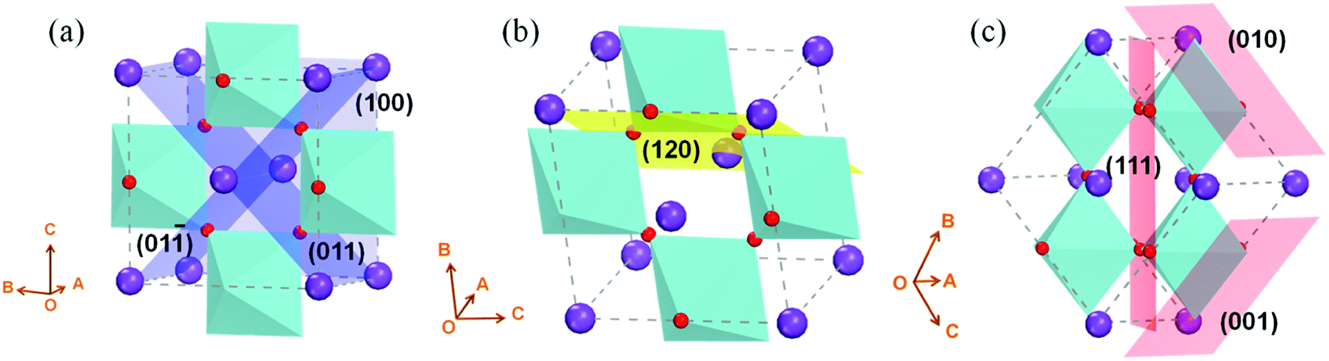 | ||
| Fig. 1 (a) (100), (011) and (01) facets of Amm2 orthorhombic KNbO3 (cut plane marked by blue) with 0° tilt of oxygen octahedrons, these three facets are perpendicular to each other, forming a cubic morphology. (b) (120) facet (cut plane marked by yellow) with 60° tilt of oxygen octahedrons, shows a pseudo-hexagonal symmetry in plane. (c) (001), (010) and (111) facets (cut plane marked by red) with 90° tilt of oxygen octahedrons. | ||
| (100) | (011) | (01) |
(001) | (010) | (111) | (120) | |
|---|---|---|---|---|---|---|---|
| Eslab − Ebulk (eV) | 11.68 | 4.68 | 3.34 | 55.68 | 40.68 | 44.68 | 51.68 |
| Surface (Å2) | 67.446 | 65.404 | 65.404 | 92.224 | 92.768 | 140.926 | 113.338 |
| Es (eV Å−2) | 0.086 | 0.033 | 0.026 | 0.298 | 0.217 | 0.158 | 0.227 |
To investigate the relevance of surface energy to surface polar properties, trilayers 2D models of KNbO3 crystal with (100)orth and (120)orth facet orientations are built. After lattice relaxation, stable 2D structures are obtained (Fig. 2a and c). Their electronic structures are calculated. Specifically, the 60° tilted facet of (120)orth 2D crystal shows an alternating valence variation of (KO3)5−/Nb5+, indicating a potential huge polar difference in alternating atomic planes, as shown in Fig. 2d. From the sliced mapping of electron localization functions (ELF) in Fig. 2b and d, quantum confined surface states can be clearly observed on both surfaces, which surround the perfectly localized core and the bonding electrons (where ELF approaches 1)23 of oxygen atoms, allowing the electron and hole carriers moving freely on the surface. In consideration of the distinct electronic reconstructions, (100)orth with extra e−/2 (N-type) and (120)orth with extra 3h+/2 (P-type) injection per unit cell, their electronic phases should be different. Fig. 3a and b show the calculated bands around EF of (100)orth and (120)orth oriented 2D KNbO3. Conventional free electron conductance switches to free hole conductance when a facet of (100)orth changes to (120)orth by the 60° tilting of oxygen octahedrons. The preferential growth facet also changes the symmetry of electronic states transitions, resulting in an indirect optical band gap transition changing to direct at Γ point, as the red arrows indicated in ESI Fig. S2a and S2b.† Density of states of s, p, d orbits (Fig. 3c and d) shows further insights of this switching behavior. The potential of low-lying conduction band descends by 0.39 eV due to extra electron injection, pushing the Nb 4d band to EF and allowing electrons to move freely at the bottom of the conduction band (Fig. 3c). Conversely, extra holes injection induced by strongly quantized O 2p states lifts the valence band by 0.17 eV above EF, giving free holes. The low-lying subbands of Nb 4d are split t2g bands, composed of a heavy (dyz doublet) and a light (dxy singlet) band.24 Strong confinement lifts up the light t2g band with respect to the heavy ones (Fig. 3a), demonstrated in the thickness dependence of band structures variations of (100)orth models (See Fig. S4†), due to the difference in me. The top O 2p bands also split into three subbands, the highest heavy (Ehb+) and underlying two light (Elb+) ones (Fig. 3b) under the quantum confined regime.
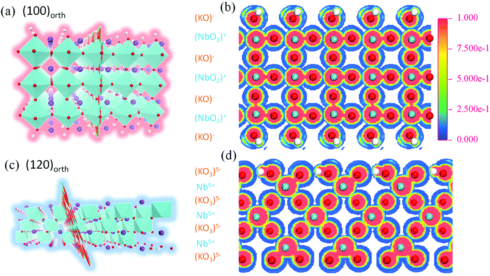 | ||
| Fig. 2 (a) and (c) The trilayers (octahedron layer) atomic structures of (100)orth and (120)orth oriented 2D KNbO3 models, surface dangling bonds of oxygen were capped by hydrogen atoms, the selected cutting slices of Nb–O plane of calculated ELF in (a) and (c) were showed in (b) and (d) by colored maps, respectively. Both of the 2D structures were obtained by energy minimization through optimizing geometry. | ||
 | ||
| Fig. 3 (a) and (b) Calculated band structures of trilayers (octahedron layer) (100)orth and (120)orth oriented 2D KNbO3 models, respectively. Free electron states switch to free holes when facets changed. (c) and (d) Partial density of states of s, p, d orbits of both of 2D KNbO3 models, respectively. Oblique fill lines show the sum of DOS of different orbits. | ||
Quantized electronic states in a 2D square quantum well
To obtain the effect of the size limitation to free electronic states, the band structures of (120)orth 2D KNbO3 with thicknesses that range from 0.23 nm (1 octahedron layer) to 4.6 nm (20 octahedron layers) are calculated (see Fig. S8†). Strong quantum confinement can be observed with a decrease in thickness, accompanied by the splitting of degenerate energy into independent sub-bands, as indicated by the red arrow in ESI Fig. S8.† A two-dimensional square quantum well is used to describe the thickness dependence of quantum confined band gaps, given by: ,25 where Eg is the calculated energy gap of the 2D model and E0g is the calculated energy gap of the bulk crystal model (E0g ∼ 2.3 eV, as shown in ESI Fig. S9†). The second term represents quantum localization, where ℏ is the reduced Planck's constant, r is the sheet thickness, and
 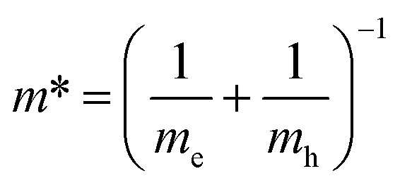 is the reduced effective mass. Fig. 4a plots the calculated thickness dependence of quantum well transition energies with dimension reduction. The value of m* is 0.6 me, which is obtained from fitting a best fit line to calculate Eg values (pink dotted line in Fig. 4a). The solid fit line in the inset confirms the linear relationship of quantum confined energies to 1/r2 for a 2D square quantum well.
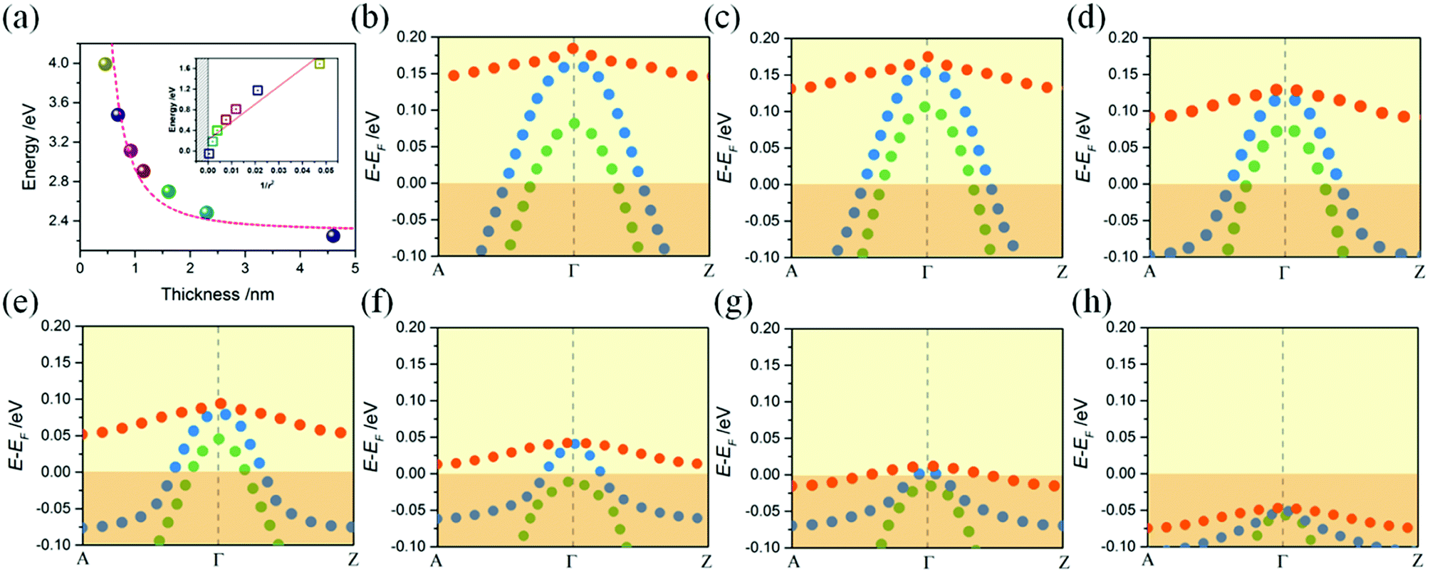 | ||
| Fig. 4 (a) Colored balls correspond to the calculated band gap energy of 2D models with thicknesses varying from 0.46 nm to 4.6 nm. The abrupt increase in band gap energy occurs at below 2 nanometer size, where there is a presence of strong quantum confinement. The theoretically calculated curve (pink dotted line) fits very well to the experimental data. Inset illustrates the linear relationship between the quantum confinement effected energy values and 1/r2. (b)–(h) The evolution of quantum localized hole states with 2D well thickness varying. Red dotted line denotes the heavy hole (Ehb+) band, blue and green dotted lines denote the two light (Elb1+ and Elb2+) bands. | ||
The hole states occupation of samples are shown in Fig. 4b–h. A monotonous decreasing relationship of confined energy of hole states with respect to the thicknesses of 2D wells is observed, where the O 2p bands will be totally under EF when thickness approaches 4.6 nm. Strong confinement leads to the splitting of the top O 2p band into one heavy (Ehb+, denoted as red dots) and two light (Elb1+ and Elb2+, denoted as blue and green dots respectively) bands at Γ point. The decrease in quantum confined energy contributes to the appearance of degenerate Ehb+ and Elb1+ bands (as shown in Fig. 4b–f), accompanied by the gradual increase of mh of Elb1+ along momentum k. Until reaching the weak confined situation (Fig. 4g), the light Elb2+ band descends down to EF first, then degenerate Ehb+ and Elb1+ bands will further combine with Elb2+ and totally descend under EF (Fig. 4h). A similar trend of low-lying conduction t2g band of (100)orth models being lifted up to EF can be observed with an increase in thickness (see ESI Fig. S5†), showing that both of 2DEG and 2DHG cases have strong quantum confinement along the Z direction.
Insulator–metal transition
To obtain further insight of the insulator–metal transition of our 2DFEG/2DFHG systems, optical absorption properties of models with varying thicknesses are calculated. Fig. 5a shows the absorption spectra of (120)orth oriented 2D KNbO3 models (thicknesses are from 0.46 nm to 4.6 nm). The strong absorption across the whole optical gap demonstrates the insulator–metal transition. Fig. 5b plots the maximum absorption of the free hole states (collected from low-frequency absorption spectra, as shown in inset figure), showing that the free holes absorption intensity increase gradually with an increase in thickness. Up to above 1.15 nm (5 layers), it decreased dramatically with an increase in thickness, indicating a critical thickness of about 2 nm for the existence of metallic states for 2DHGs. A gradual blue-shift of intrinsic absorption band edges can be observed when the number of layers increases (indicated by the blue arrow in Fig. 5a), along with one single peak extending to two individual peaks (as pink arrow indicated in Fig. 5a) due to the splitting and lifting of s, p orbits from the degenerate d band (Fig. 5c). This agrees with the quantized characters of conduction band in 2D quantum well. Although the occupation energy of hole states above EF decreases with an increase in well thickness (such as the pink arrow marked in Fig. 5c and blue arrow marked in Fig. 5d), the increase of DOS near EF (marked by pink arrow in Fig. 5d) competes with the decrease of confined energy, leading to an increase initially then decrease of free hole states absorptions. The increase in DOS near EF is ascribed to the increased total numbers of atoms per unit area when stacking layers increase. However, the confined energy still plays a dominant role for metallic states maintaining, as plotted in Fig. 4b. The absorption properties of free electrons ((100)orth oriented 2D KNbO3 models) show a similar trend of confined states transition while the thickness variation (see ESI Fig. S6a†), although the ∼4 nm (10 layers) model shows an anomalous absorption in the low-frequency range, which can be ascribe to the abrupt increase of the local DOS near EF, as marked by pink arrow in ESI Fig. S6b.†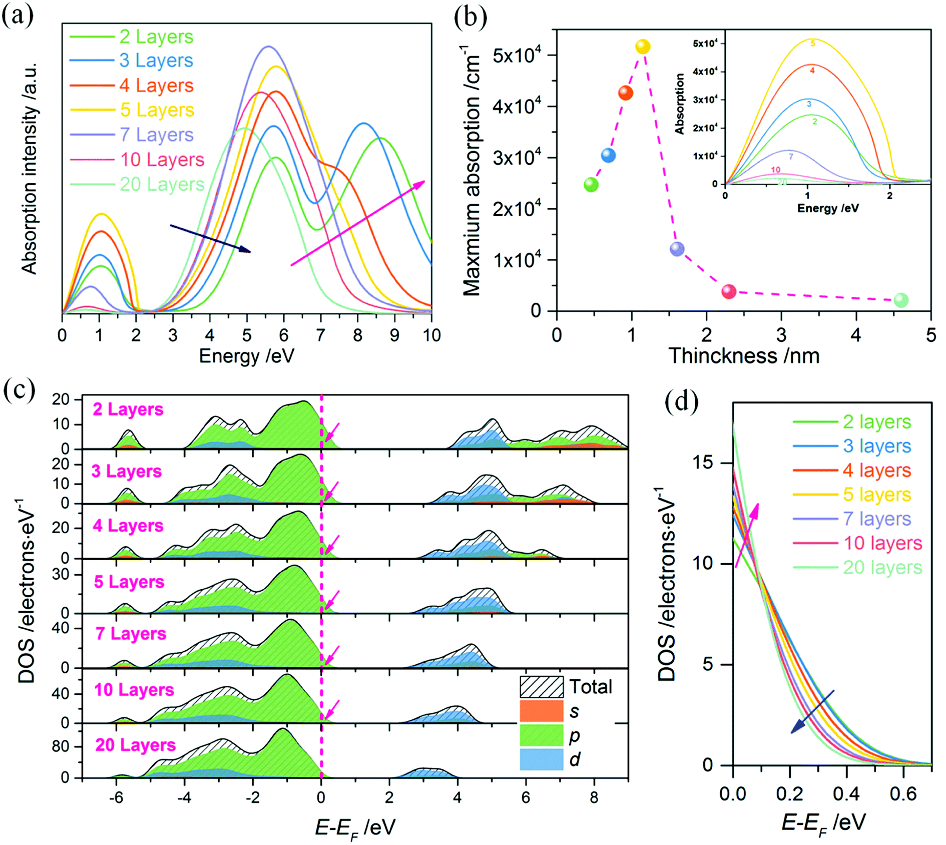 | ||
| Fig. 5 (a) Absorption properties of (120)orth oriented 2D KNbO3 models, the absorption in low frequency indicates an insulator–metal transition absorption. (b) The thickness dependences of absolute absorption intensity of free hole states, inset is the zoom in of low-frequency range. (c) PDOS of (120)orth oriented 2D KNbO3 with thickness range from 2 layers to 20 layers, show the thickness dependence of quantum localized free holes and the corresponding contributions of different orbits. (d) Evolution trend of quantized hole states with respect to the thickness varying. The quantum localized energy and the absolute value of electronic states per electron volt co-work on the free hole states absorption, showing a converse contribution (as the blue and pink arrows indicating with reverse directions). | ||
Conclusions
In summary, beyond well-known concepts for rearranging these surface electronic states (with extra electrons injecting) in 2D heterointerface or bare surface, our results show that additional holes injection can be maintained by the increase of surface polarity. The 2DEGs/2DHGs switching can be simply fulfilled by facet orientations. Distinct orientations change the polar discontinuity of alternating atom layers, corresponding to that huge surface energy differences. The thickness dependent behaviors of free electron/hole states subjecting to quantum confinement are addressed by the varied thickness of 2D models. Compared with free electron states induced insulator–metal transition (4 nm sample still exists strong free electron states absorption), free hole states transition depends much stronger on the thickness of 2D quantum well, with a small critical value of ∼2 nm. The formation of free electrons is more complex than free holes (contributed by O 2p states) due to the hybridization of s, p, d orbits in conduction bands. Such as one p band abnormally extends under EF (among the split t2g bands) for (100)orth oriented monolayer model at the extreme confined regime, acting to form an additional free electron conduction band (see ESI Fig. S5a†). Despite their differences, both of 2DEGs and 2DHGs are resulted from strong quantum confinement. Furthermore, the confined energy (E − EF) and the total DOS occupying near EF (which varies with sample thickness) jointly act on the metallic state transition, demonstrating that metallic states can be modulated not only by the amount of donor-like defects or adsorbates, but also simply by thickness variation.In contrast to previous theoretical and experimental results,3,4,24,26 our theoretical study reveals that the free holes can be obtained on high polar surface of perovskite oxides, gives the origins of oxides 2DEGs/2DHGs, including their intrinsic switching by surface polarity change and confined evolution behaviors with respect to quantum well thickness, emerging as a promising basis towards design the new generation all-oxides electronic devices.
Conflicts of interest
There are no conflicts to declare.Acknowledgements
The work at HIT is supported by the Fundamental Research Funds for the Central Universities. Grant No. Hit. KISTP. 201401.References
- E. E. Mendez, L. Esaki and L. L. Chang, Phys. Rev. Lett., 1985, 55, 2216 CrossRef PubMed.
- J. M. Kikkawa, Science, 1997, 277, 1284–1287 CrossRef.
- A. Ohtomo and H. Y. Hwang, Nature, 2004, 427, 423–426 CrossRef PubMed.
- W. Meevasana, P. D. C. King, R. H. He, S.-K. Mo, M. Hashimoto, A. Tamai, P. Songsiriritthigul, F. Baumberger and Z.-X. Shen, Nat. Mater., 2011, 10, 114–118 CrossRef PubMed.
- A. F. Santander-Syro, O. Copie, T. Kondo, F. Fortuna, S. Pailhes, R. Weht, X. G. Qiu, F. Bertran, A. Nicolaou, A. Taleb-Ibrahimi, P. Le Fevre, G. Herranz, M. Bibes, N. Reyren, Y. Apertet, P. Lecoeur, A. Barthelemy and M. J. Rozenberg, Nature, 2011, 469, 189–193 CrossRef PubMed.
- C. Cen, S. Thiel, J. Mannhart and J. Levy, Science, 2009, 323, 1026–1030 CrossRef PubMed.
- S. Okamoto and A. J. Millis, Nature, 2004, 428, 630–633 CrossRef PubMed.
- C. Cen, S. Thiel, G. Hammerl, C. W. Schneider, K. E. Andersen, C. S. Hellberg, J. Mannhart and J. Levy, Nat. Mater., 2008, 7, 298–302 CrossRef PubMed.
- N. Reyren, S. Thiel, A. D. Caviglia, L. F. Kourkoutis, G. Hammerl, C. Richter, C. W. Schneider, T. Kopp, A. S. Ruetschi, D. Jaccard, M. Gabay, D. A. Muller, J. M. Triscone and J. Mannhart, Science, 2007, 317, 1196–1199 CrossRef PubMed.
- A. Brinkman, M. Huijben, Z. M. Van, J. Huijben, U. Zeitler, J. C. Maan, V. D. W. Wg, G. Rijnders, D. H. Blank and H. Hilgenkamp, Nat. Mater., 2007, 6, 493–496 CrossRef PubMed.
- S. Banerjee, O. Erten and M. Randeria, Nat. Phys., 2013, 9, 625–629 CrossRef.
- A. F. Santander-Syro, F. Fortuna, C. Bareille, T. C. Rödel, G. Landolt, N. C. Plumb, J. H. Dil and M. Radović, Nat. Mater., 2014, 13, 1085 CrossRef PubMed.
- N. C. Plumb, M. Salluzzo, E. Razzoli, M. Månsson, M. Falub, J. Krempasky, C. E. Matt, J. Chang, M. Schulte and J. Braun, Phys. Rev. Lett., 2014, 113, 086801 CrossRef PubMed.
- M. Huijben, G. Rijnders, D. H. Blank, S. Bals, S. Van Aert, J. Verbeeck, G. Van Tendeloo, A. Brinkman and H. Hilgenkamp, Nat. Mater., 2006, 5, 556–560 CrossRef PubMed.
- Y. Chen and N. Pryds, Nat. Mater., 2018, 17, 215–216 CrossRef PubMed.
- H. Lee, N. Campbell, J. Lee, T. J. Asel, T. R. Paudel, H. Zhou, J. W. Lee, B. Noesges, J. Seo and B. Park, Nat. Mater., 2018, 17, 231–236 CrossRef PubMed.
- W. Lu, J. Xiang, B. P. Timko, Y. Wu and C. M. Lieber, Proc. Natl. Acad. Sci. U. S. A., 2005, 102, 10046 CrossRef PubMed.
- K. Nomura, J. Wunderlich, J. Sinova, B. Kaestner, A. H. MacDonald and T. Jungwirth, Phys. Rev. B, 2005, 72, 245330 CrossRef.
- R. Moriya, K. Sawano, Y. Hoshi, S. Masubuchi, Y. Shiraki, A. Wild, C. Neumann, G. Abstreiter, D. Bougeard and T. Koga, Phys. Rev. Lett., 2014, 113, 2916–2921 CrossRef PubMed.
- M. D. Segall, P. J. D. Lindan, M. J. Probert, C. J. Pickard, P. J. Hasnip, S. J. Clark and M. C. Payne, J. Phys.: Condens. Matter, 2002, 14, 2717 CrossRef.
- J. P. Perdew, K. Burke and M. Ernzerhof, Phys. Rev. Lett., 1996, 77, 3865–3868 CrossRef PubMed.
- Y. Bi, S. Ouyang, N. Umezawa, J. Cao and J. Ye, J. Am. Chem. Soc., 2011, 133, 6490–6492 CrossRef PubMed.
- B. Silvi and A. Savin, Nature, 1994, 371, 683–686 CrossRef.
- P. Delugas, A. Filippetti, V. Fiorentini, D. I. Bilc, D. Fontaine and P. Ghosez, Phys. Rev. Lett., 2011, 106, 166807 CrossRef PubMed.
- L. E. Brus, J. Chem. Phys., 1984, 80, 4403–4409 CrossRef.
- Z. S. Popović, S. Satpathy and R. M. Martin, Phys. Rev. Lett., 2008, 101, 256801 CrossRef PubMed.
Footnote |
| † Electronic supplementary information (ESI) available: Computation methods, surface slabs of different facets of KNbO3, band structure of trilayers models of 2D KNbO3, crystal models of (100)orth oriented 2D KNbO3, band structures of (100)orth oriented 2D crystal, states occupation below EF of (100)orth oriented 2D crystals, free electrons absorptions of (100)orth oriented 2D KNbO3, crystal models of (120)orth oriented 2D crystal, band structures of (120)orth oriented 2D crystal, electronic structures of bulk KNbO3 crystal (PDF). See DOI: 10.1039/c8ra03928c |
| This journal is © The Royal Society of Chemistry 2018 |