
 Open Access Article
 This Open Access Article is licensed under a Creative Commons Attribution-Non Commercial 3.0 Unported Licence
Development of a candidate reference sample for the characterization of tip-enhanced Raman spectroscopy spatial resolution†
Alessio Sacco ab,
Dario Imbraguglioa,
Andrea M. Giovannozzia,
Chiara Portesi*a and
Andrea M. Rossia
ab,
Dario Imbraguglioa,
Andrea M. Giovannozzia,
Chiara Portesi*a and
Andrea M. Rossia
aIstituto Nazionale di Ricerca Metrologica, Torino, 10135, Italy. E-mail: c.portesi@inrim.it
bPolitecnico di Torino, Torino, 10129, Italy
First published on 3rd August 2018
Abstract
Tip-Enhanced Raman Spectroscopy (TERS) is a topographic and chemical analysis technique with nanoscale resolution, consisting of the combination of Scanning Probe Microscopy (SPM) and Localized Surface Plasmon Resonance (LSPR) for the enhancement of Raman scattering in the vicinity of the probe. The quantification of spatial resolution represents an important issue, and, as of now, standards for calibration are not available. In the present work a candidate reference sample for TERS measurements was fabricated. It consists of a flat, conductive gold surface with a nanometric grating of a self-assembled monolayer of Raman-active organic molecules fabricated by an optimized Electron Beam Lithography (EBL) method to replicate established SPM calibration standards. Its feasibility as a TERS standard was tested by STM-TERS imaging.
Introduction
Industry and scientific research rely upon the ability to determine quantities accurately and unequivocally and, to achieve that, establishing common guidelines for measurements and reference samples for calibration is important. Metrology tackles this issue to provide the basis for a single, coherent system of measurements throughout the world, traceable to the International System of Units (SI), with the respective universal practical realisation of the units and methods of measurement.Raman spectroscopy is an analytical technique with increasing industrial applications, but it currently lacks reference materials. The application of certified reference materials (CRMs) in analytical chemistry for quality control purposes is well recognized and recommended by a wide range of international, national and professional organizations. In this work we propose a fabrication method for a candidate reference sample for spatial resolution calibration of Tip-Enhanced Raman spectroscopy (TERS) setups. TERS combines plasmon-enhanced Raman spectroscopy and scanning probe microscopy (SPM), a technique which has been developed to measure spatial features of surfaces with nanometric resolution, allowing simultaneous chemical and topographic mapping of surfaces with nanometric resolution.1–5
In SPM, a tip with a sharp apex allows probing of areas a few nanometres wide and the reconstruction of topographic images with spatial resolution much higher than conventional optical microscopy. Indeed, the latter is diffraction-limited, making it impossible to resolve features smaller than approximately half of the light wavelength (for visible light, no less than about 200 nm), while SPM can achieve atomic spatial resolution depending on the characteristics of the probe, the feedback and the apparatus employed.
In a TERS setup, a metallic SPM tip is illuminated by a laser beam. The emitted signal is collected by a microscope objective and analysed by a Raman spectrophotometer. By combining the two techniques, it is possible to register topographic and chemical maps, each with a spatial resolution (usually quantified by the ability to spatially resolve two adjacent targets, or by calculating the FWHM of the profile of a sharp feature in the image) dictated by the probe apex and comparable to its nanometric dimensions.6–11 To achieve TERS, the surface plasmons on the probe tips must resonate with the excitation laser electromagnetic frequency so that a plasmonically enhanced, Raman-amplifying electromagnetic field is formed, and is localised in the vicinity of the tip apex.1 This physical phenomenon is the same as in surface-enhanced Raman spectroscopy, but in TERS the Raman signal amplification is bound to a single, restricted region (a hotspot), from which the SPM feedback also arises. Raman-amplifying SPM probes may be fabricated by either coating a classical SPM probe with an appropriate metal, or by shaping a probe from solid metal such as a wire (silver or gold are widespread choices for visible excitation wavelengths).
Even though in the literature many significant results have been obtained by exploiting TERS capabilities, including single-molecule and ultrafast mapping, and TERS has been applied to diverse environments such as ultrahigh vacuum and liquids,12–14 one of the most urgent issues is related to the questions about reproducibility of the results and the standardization of the methods. Actually, while metrological SPMs have been already developed, the way towards metrological TERS has yet to be paved. By metrological SPM, it is possible to trace three-dimensional length measurements to the length SI standard with nanometric accuracy.15,16 By metrologically calibrated TERS, the chemical information will be traceable to the SI as well and, at the same time, the measurements will gain in terms of reproducibility.
In this paper, a candidate sample suitable to achieve TERS chemical imaging traceability to the metre by means of an SPM-based calibration procedure for nanometric accuracy is presented. It is designated to be both highly thermally and electrically conductive to minimise radiation heating and for measurements with both force-based and tunnelling current TERS feedbacks, making it a suitable candidate to be a universal TERS standard for calibration and comparisons, regardless of the apparatus specifications.17 Its gold surface, albeit flat, further enhances TERS signals, leading to measurements in gap-mode, resulting in much more intense signals than those arising from a non-gap mode TERS measurement,18 and a much lower detection limit.19 The sample is characterised during the different steps of the production process with several techniques, including confocal Raman, AFM, and TERS imaging in STM feedback.
Experimental
Sample
The sample was manufactured as described in Fig. 1, starting from a clean SiO2/Si surface (280 nm SiO2 on monocrystalline Si, by Si-Mat). 20 nm of gold (99.999%, Alfa Aesar) were deposited by electron-gun evaporation at a rate of 0.1 nm s−1 after the deposition of 5 nm of titanium (99.99%, Alfa Aesar) as adhesion layer. The resulting surface was then covered by 50 nm of poly methyl-methacrylate (PMMA) by spin-coating (at 6000 rpm for 60 s) to form the electron-sensitive layer. The Electron Beam Lithography (EBL) was performed with a dose of 670 μC cm−2 and an acceleration voltage of 30 kV. Afterwards, it was developed in methyl isobutyl ketone (MIBK in isopropyl alcohol 1![[thin space (1/6-em)]](https://www.rsc.org/images/entities/char_2009.gif) :3) for 30 s, then rinsed in IPA and water and dried with nitrogen. The nanostructured samples were then soaked either in thiophenol solution (TP, ≥99% from Sigma-Aldrich, 5 mM in ethanol) or in 7-mercapto-4-methylcoumarin (MMC, ≥97% from Sigma-Aldrich) solution (1 mM in ethanol) for 18 h, resulting in the formation of thiol Self-Assembled Monolayers (SAM)20,21 selectively bonded on the exposed Au portion of the sample. The specimens were then thoroughly rinsed in ethanol and dried with nitrogen. At the end, to remove the PMMA resist, the samples were sonicated in acetone (≥99.8%, Carlo Erba) for 5 minutes (37 kHz at 30 °C), rinsed with ethanol and nitrogen flux dried.
:3) for 30 s, then rinsed in IPA and water and dried with nitrogen. The nanostructured samples were then soaked either in thiophenol solution (TP, ≥99% from Sigma-Aldrich, 5 mM in ethanol) or in 7-mercapto-4-methylcoumarin (MMC, ≥97% from Sigma-Aldrich) solution (1 mM in ethanol) for 18 h, resulting in the formation of thiol Self-Assembled Monolayers (SAM)20,21 selectively bonded on the exposed Au portion of the sample. The specimens were then thoroughly rinsed in ethanol and dried with nitrogen. At the end, to remove the PMMA resist, the samples were sonicated in acetone (≥99.8%, Carlo Erba) for 5 minutes (37 kHz at 30 °C), rinsed with ethanol and nitrogen flux dried.
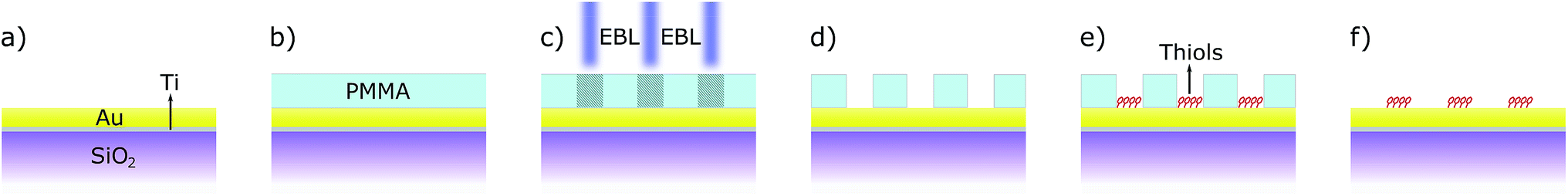 | ||
| Fig. 1 Scheme of the steps of the standard production process. The initial flat 20 nm Au surface (a), deposited on SiO2 with a Ti adhesion layer, is covered by a 50 nm PMMA mask (b), which is then selectively exposed to EBL (c). After the mask development, bare Au areas remain (d), where thiols can selectively bond. The surface is soaked in a thiol solution until a self-assembled monolayer is formed (e), then rinsed, and sonicated in acetone to remove the mask. After this process, the gold surface with a nanopatterned thiol SAM is ready (f). | ||
Apparatus
TERS measurements were performed in ambient conditions and in STM feedback with a NT-MDT Ntegra scanning probe microscope, equipped with a 10 μm × 10 μm piezoelectric scanner and customised with mirrors to allow tip illumination and scanning of the Raman laser excitation source (He–Ne 633 nm, electrically pumped, continuous, linearly polarized) from a modified Thermo DXR spectrometer, responsible for the spectra acquisition as well. The system achieves 5 cm−1 spectral resolution in the 50–3600 cm−1 spectral range. Illumination of the tip and signal collection is mediated by a 100×, long working distance microscope objective (Mitutoyo M Plan Apo 100, 0.7 NA) in a top illumination configuration (Fig. 2).22 The TERS tips were fabricated by electrochemical etching of a 0.25 mm diameter Ag wire (99.99% purity, from Sigma-Aldrich) in a 1:2 v/v solution of perchloric acid (70% HClO4 in water, from Merck) in methanol (special grade, by Carlo Erba) by applying a (8.1 ± 0.1) V voltage difference with respect to a circular Au cathode.23–25 This mechanism was electronically controlled by a homemade feedback circuit that automatically cut the voltage after the wire drop-off and the tips were formed, standardising the procedure to make it operator-independent in order to obtain apices whose curvature radii were centred around 40 nm, with a dispersion of 10 nm. AFM measurements were performed using the Ntegra SPM, in semi-contact mode in order not to modify the structure of the PMMA, using uncoated NT-MDT VIT-P top visual Si probes (resonant frequency ∼300 kHz). Confocal Raman measurements were carried out using the TERS apparatus without the tip mounted or with the out of focus tip when reported. TERS chemical intensity maps were calculated by measuring the area of the Lorentzian functions best fitting the peaks in the ±50 cm−1 spectral region centred on the wavenumber of the signal on which the map is based, after background subtraction. The enhancement factors reported were calculated by measuring the height of the fitted Raman signal used for the calculation after background subtraction; when noise was considered, the standard deviation of the noise in the 1750–2250 cm−1 region (after background subtraction) was utilised.
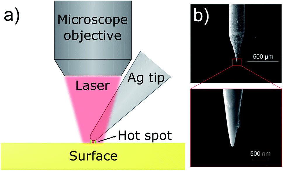 | ||
| Fig. 2 (a) scheme of the top visual TERS apparatus employed in the measurements; (b) SEM image of a STM-TERS silver tip fabricated by the electrochemical etching. | ||
Results and discussion
Mask characterization
Preliminary measurements with both STM and confocal Raman verified that the Au/Ti evaporated surfaces are fully conductive and completely Raman inactive after thiophenol deposition. AFM tests and following characterizations also demonstrated that these substrates have a low roughness (ISO 4287 parameters for surface roughness: Sq = 2.3 nm, Sa = 1.8 nm). Moreover, they are robust enough to withstand vigorous AFM measurements in full contact, and mask deposition and lift-off by sonication. While it is possible to draw any kind of patterns onto the mask, simple and regular geometries are desirable for its use as a calibration standard.26,27 Repeating long, straight, parallel lines in a known direction respectively to the Si wafer were chosen in this study. Different EBL doses and varied line spacing were employed in order to establish the appropriate conditions for proper exposure, avoiding incomplete development due to insufficient doses, as well as averting overexposure and distortion/merging of pattern elements by determining the minimum line distance at which distinct features subsist when doses adequate for full exposure are employed.After development with MIBK, the samples were measured with semi-contact AFM. In Fig. 3, an AFM map of the optimised mask is shown; since the mask height is 50 nm, trench depths below this value are to be considered underdeveloped, since the Au surface below is necessarily covered by PMMA. After several dose experiments a dose of 670 μC cm−2 has been chosen as optimal for the fabrication of a reliable mask with predictable bare Au areas for subsequent thiol chemically selective bonding.
 | ||
| Fig. 3 AFM image (a) of a PMMA mask exposed to the ideal EBL dose of 670 μC cm−2, measured after development: the gold surface underneath the mask is exposed, yet the lines are still separate; a line profile taken on the blue line is reported in (b). | ||
TERS imaging
TERS chemical imaging in STM mode was performed on the finalised samples in order to verify the presence and the integrity of the monolayers, and that the masks were completely removed by the treatment. This was proven by the fact that no PMMA signal was measured on the surfaces. Moreover it was verified that the portions of the surfaces that were supposed to remain pristine (because of the mask coverage and subsequent lift-off) were actually free of thiols, and that the molecules had not diffused onto them instead.In Fig. 4, a TERS chemical map of one of the thiophenol patterned surfaces is shown, the red colour representing the 1074 cm−1 peak intensity (νCC + δCH).17 Very recognisable parallel lines, corresponding to the spatial features previously measured on the PMMA masks, are clearly visible, and interspersed with zones with near zero intensity. An investigation of the corresponding spectra shows that no chemical was detected on these black areas, while pure benzenethiol spectra are registered on the lines corresponding to the organic pattern.
 | ||
| Fig. 4 STM-TERS chemical map (a), without corrections, based on the 1074 cm−1 Raman peak, of a nanopatterned thiophenol surface, obtained with 0.25 mW laser power and 0.5 s per pixel integration time (pixel size ∼7.5 nm), and a line profile based on this signal (b), taken on the dashed line in (a). Raman spectra corresponding to the map are reported: a TERS spectrum on a SAM-covered area (c); a TERS spectrum corresponding to a bare gold pixel (d); a confocal Raman spectrum of the sample, measured with the tip retracted from the surface (e). The marks on the map indicate the pixels where the spectra (c) and (d) were taken. | ||
In order to test the limits of the our sample production process, a thinner pattern was drawn and a grating of thiophenol with lines roughly 8 nm wide were obtained. The resulting TERS chemical map of the 1074 cm−1 Raman shift can be seen in Fig. 5: lines with width of (9 ± 4) nm were measured (the line width is defined here as the mean and standard deviation of the FWHMs of the Gaussian interpolations of several intensity profiles along the scans). The map was measured with a 7.5 nm pixel size: by the Shannon–Nyquist theorem, faithful sampling cannot be performed at a rate lower than the Nyquist rate (i.e. half the lateral dimensions of the features, or about 16 nm in this case), hence the reconstructed lines are prone to strong aliasing.
 | ||
| Fig. 5 STM-TERS raw chemical map of the 1074 cm−1 thiophenol peak on a nanopatterned substrate obtained from a partially underexposed map in order to reduce the pattern thickness below the beam diameter of the EBL. It was acquired with 0.25 mW laser power and 0.5 s integration time per pixel (pixel size ∼7.5 nm). | ||
Thiophenol is a widely used molecule in plasmon-enhanced Raman studies,17 but the aforementioned patterning approach was investigated for the application to a different thiol as well. The chosen molecule was 7-mercapto-4-methylcoumarine (MMC), a relatively unexplored molecule in TERS that was found to yield much more intense plasmon-enhanced Raman signals than thiophenol. In Fig. 6, a TERS chemical map of the nanopatterned MMC sample after mask lift-off is shown, coloured based on the intensity of the 1593 cm−1 MMC C![[double bond, length as m-dash]](https://www.rsc.org/images/entities/char_e001.gif) C stretching band.28,29 Nevertheless, this map exhibits feeble MMC signals in areas that were covered during the molecule deposition step of the fabrication process, suggesting lesser stability of the monolayer during the mask lift-off process, or because of tip contamination during the TERS measurement, or both.
C stretching band.28,29 Nevertheless, this map exhibits feeble MMC signals in areas that were covered during the molecule deposition step of the fabrication process, suggesting lesser stability of the monolayer during the mask lift-off process, or because of tip contamination during the TERS measurement, or both.
 | ||
| Fig. 6 STM-TERS chemical image (a), without corrections of a MMC-patterned sample, based on the 1593 cm−1 CC stretching mode. The acquisition conditions are 0.25 mW laser power and 0.5 s per pixel as exposure time, step size ∼8 nm. A line profile based on the intensity of this peak over the dashed line is shown in (b). Raman spectra of the sample with the same conditions are also reported: a TERS spectrum of the SAM (c); a spectrum of an area previously covered by the PMMA mask (d); a confocal Raman spectrum of the sample after the retraction of the tip (e). Marks on (a) correspond to the points where the spectra (c) and (d) were measured. | ||
Beside the spatial distribution, the Enhancement Factor (EF) can be estimated too from the TERS maps. The EF is often defined30,31 as the factor by which the Raman effect is amplified by the tip in the effective hotspot area, hence:
 | (1) |
 | (2) |
The lower EF limits were found to be EF > (2.2 ± 0.5) × 107 for thiophenol, and EF > (1.0 ± 0.2) × 108 in the case of MMC. In surface- and tip-enhanced Raman spectroscopy, it is common to be unable to resolve a non-enhanced signal from the confocal Raman measurements. A formula for the EF estimation in such a case, adapted from29 for TERS, is the following:
 | (3) |
A comparison between the TERS chemical and topographic images on these substrates can be carried out in order to extract dimensional information about the probe chemical capabilities. The aforementioned line patterns are quite practical for this purpose, because measuring the lines width in both maps is straightforward, and it generates a large sample size, given that each scan can be considered an independent measurement. In Fig. 7, the topographic and chemical TERS maps of the same sample area are shown, with the corresponding statistical analysis. While the sample is flat and the SAM lines have modest thickness, quite noticeable trenches are visible in the topographic map. This is due to the difference in conductivity between the naked, previously masked gold areas and the SAM areas on gold: in a constant current STM map such as this, less conductive areas on a flat sample are registered as spatially lower because of the tip movement necessary to maintain the feedback. Each thiol line and tip scan were considered as independent measurements of the same quantity, namely the line width defined as the distance between the two edges at 10% of the maximum intensity (in the chemical map) or depth (for the STM map). The lines have a mean width of μ = 25.9 nm with a standard deviation of σ = 3.5 nm in the STM measurement, and a mean of μ = 28.1 nm with σ = 3.9 nm standard deviation in the chemical image. This indicates a larger line width in the chemical map, most likely caused by the larger effective probe size: while a probe used in STM can be approximated to have apex dimensions of a few Å, with a similar interaction radius with the surface,33 TERS hotspots are significantly broader. An SPM spatial measurement yields the convolution of the target feature with the tip shape and size, therefore these findings are consistent with the expected effects.
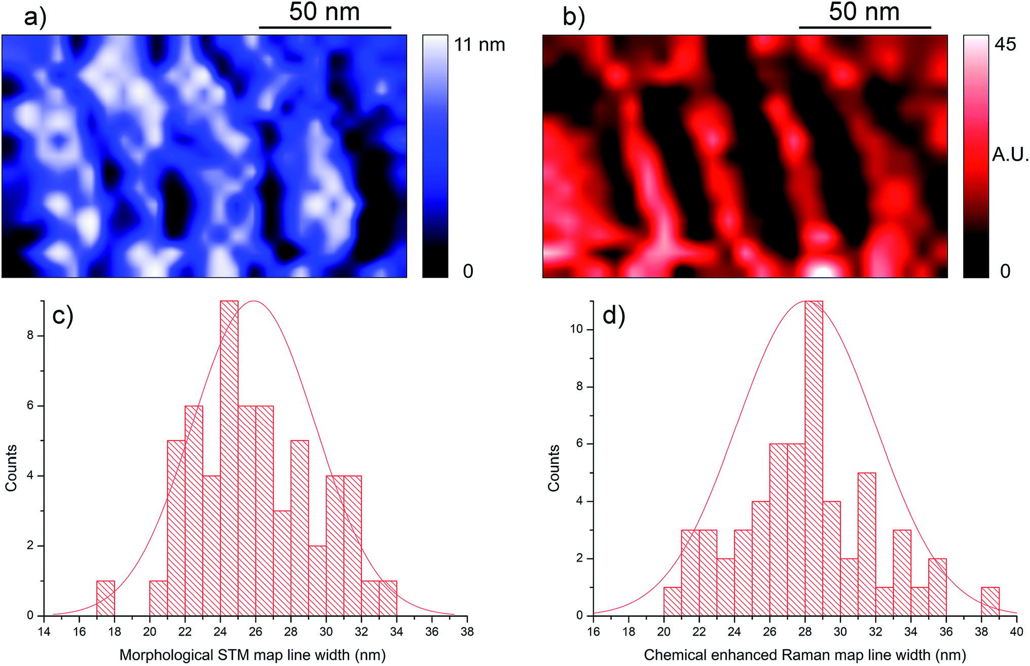 | ||
| Fig. 7 Comparison of topographic (a) and chemical (b) images of an area of the proposed sample, acquired concurrently by STM-TERS. The image was acquired with a tunneling current feedback of 0.5 nA at 0.1 V, a laser power of 0.25 mW, 0.5 s per pixel (∼8 nm pixel size). The chemical image is based on the intensity of the 1593 cm−1 MMC peak. (c and d): statistical analysis of the thiol lines width measured in the top maps and superimposed Gaussian distribution curves with the samples means and standard deviations as parameters. Line width in the topographic map: mean μ = 25.9 nm and standard deviation σ = 3.5 nm. Line width in the chemical map: mean μ = 28.1 nm and standard deviation σ = 3.9 nm. | ||
Conclusions
In the present work, a candidate reference sample for calibration of TERS spatial resolution was proposed, consisting of a flat gold surface with customizable thiol monolayer nanopatterns; this sample is expected to be suitable for both STM and force-based TERS feedbacks (AFM, shear force microscopy). The ideal conditions for its fabrication were found by AFM measurements during production, and the final product was tested with TERS mapping in STM mode. To test the extent of its customizability, both a proven TERS model molecule, thiophenol, and a novel thiol for TERS measurements, 7-mercapto-4-methylcoumarin, were used for the fabrication of the substrates. The benzenethiol surfaces were found to be very stable, and the expected pattern was measured with a quite good Raman signal. The MMC monolayer was found to have a much greater TERS signal with respect to the thiophenol SAM: the former molecule was measured to have an EF lower limit more than 4 times larger than that of the latter; however, the measurements suggest that the stability of the MMC system is somewhat lower than those of the thiophenol SAM. A numerical comparison between the topographic and chemical components of a TERS image was performed as well. The low dispersion of the thiol lines in both the physical and chemical image of the nanopatterned monolayer, as well as the accordance of these measurements to the predictions, indicate that this substrate is a viable candidate reference sample for the calibration and comparison of TERS spatial resolution.Conflicts of interest
There are no conflicts to declare.Acknowledgements
The project 15HLT01 MetvBadBugs has received funding from the EMPIR programme co-financed by the Participating States and from the European Union's Horizon 2020 research and innovation programme.References
- S. Kawata and V. M. Shalaev. Tip enhancement, Elsevier, 2011 Search PubMed.
- R. M. Stöckle, Y. D. Su, V. Deckert and R. Zenobi, Nanoscale chemical analysis by tip-enhanced Raman spectroscopy, Chem. Phys. Lett., 2000, 318, 131–136 CrossRef.
- N. Hayazawa, Y. Inouye, Z. Sekkat and S. Kawata, Metallized tip amplification of near-field Raman scattering, Opt. Commun., 2000, 183, 333–336 CrossRef.
- N. Lee, R. D. Hartschuh, D. Mehtani, A. Kisliuk, J. F. Maguire, M. Green, M. D. Foster and A. P. Sokolov, High contrast scanning nano-Raman spectroscopy of silicon, J. Raman Spectrosc., 2007, 38, 789–796 CrossRef.
- R. Zhang, Y. Zhang, Z. C. Dong, S. Jiang, C. Zhang, L. G. Chen, L. Zhang, Y. Lia, J. Aizpurua, Y. Luo, J. L. Yang and J. G. Hou, Chemical mapping of a single molecule by plasmon-enhanced Raman scattering, Nature, 2013, 498, 82–86 CrossRef PubMed.
- M. S. Anderson, Locally enhanced Raman spectroscopy with an atomic force microscope, Appl. Phys. Lett., 2000, 76, 3130–3132 CrossRef.
- N. Kumar, S. J. Spencer, D. Imbraguglio, A. M. Rossi, A. J. Wain, B. M. Weckhuysenb and D. Roy, Extending the plasmonic lifetime of tip-enhanced Raman spectroscopy probes, Phys. Chem. Chem. Phys., 2016, 18, 13710–13716 RSC.
- C. C. Neacsu, J. Dreyer, N. Behr and M. B. Raschke, Scanning-probe Raman spectroscopy with single-molecule sensitivity, Phys. Rev. B: Condens. Matter Mater. Phys., 2006, 73, 193406 CrossRef.
- C. Zhang, B. Chen and Z. Li, Optical Origin of Subnanometer Resolution in Tip-Enhanced Raman Mapping, J. Phys. Chem. C, 2015, 119, 11858–11871 CrossRef.
- F. Latorre, S. Kupfer, T. Bocklitz, D. Kinzel, S. Trautmann, S. Gräfea and V. Deckert, Spatial resolution of tip-enhanced Raman spectroscopy – DFT assessment of the chemical effect, Nanoscale, 2016, 8, 10229–10239 RSC.
- X. Wang, S.-C. Huang, T.-X. Huang, H.-S. Su, J.-H. Zhong, Z.-C. Zeng, M.-H. Li and B. Ren, Tip-enhanced Raman spectroscopy for surfaces and interfaces, Chem. Soc. Rev., 2017, 46, 4020–4041 RSC.
- Y. Fang, Z. Zhang and M. Sun, High vacuum tip-enhanced Raman spectroscope based on a scanning tunneling microscope, Rev. Sci. Instrum., 2016, 87, 033104 CrossRef PubMed.
- Z. Zhang., S. Sheng, R. Wang and M. Sun, Tip-Enhanced Raman Spectroscopy, Anal. Chem., 2016, 88, 9328–9346 CrossRef PubMed.
- Z. Zeng, S. Huang, D. Wu, L. Meng, M. Li, T. Huang, J. Zhong, X. Wang, Z. Yang and B. Ren, Electrochemical Tip-Enhanced Raman Spectroscopy, J. Am. Chem. Soc., 2015, 137, 11928–11931 CrossRef PubMed.
- V. Korpelainen, Traceability for nanometre scale measurements: atomic force microscopes in dimensional nanometrology, PhD thesis, Department of Physics, University of Helsinki, Finland, 2014.
- R. Breil, T. Fries, J. Garnaes, J. Haycocks, D. Hußser, J. Joergensen, W. Kautek, L. Koenders, N. Kofod, K. R. Koops, R. Korntner, B. Lindner, W. Mirandeé, A. Neubauer, J. Peltonen, G. B. Picotto, M. Pisani, H. Rothe, M. Sahre, M. Stedman and G. Wilkening, Intercomparison of scanning probe microscopes, Precis. Eng., 2002, 26, 296–305 CrossRef.
- C. Blum, L. Opilik, J. M. Atkin, K. Braun, S. B. Kämmer, V. Kravtsov, N. Kumar, S. Lemeshko, J. Li, K. Luszcz, T. Maleki, A. J. Meixner, S. Minne, M. B. Raschke, B. Ren, J. Rogalski, D. Roy, B. Stephanidis, X. Wang, D. Zhang, J. Zhong and R. Zenobi, Tip-enhanced Raman spectroscopy-an interlaboratory reproducibility and comparison study, J. Raman Spectrosc., 2014, 45, 22–31 CrossRef.
- J. Stadler, B. Oswald, T. Schmid and R. Zenobi, Characterizing unusual metal substrates for gap-mode tip-enhanced Raman spectroscopy, J. Raman Spectrosc., 2013, 44, 227–233 CrossRef.
- G. Picardi, M. Chaigneau and R. Ossikovski, High resolution probing of multi wall carbon nanotubes by tip enhanced Raman spectroscopy in gap-mode, Chem. Phys. Lett., 2009, 469, 161–165 CrossRef.
- C. D. Bain and G. M. Whitesides, Formation of monolayers by the coadsorption of thiols on gold: variation in the length of the alkyl chain, J. Am. Chem. Soc., 1989, 111, 7164–7175 CrossRef.
- J. C. Love, L. A. Estroff, J. K. Kriebel, R. G. Nuzzo and G. M. Whitesides, Self-Assembled Monolayers of Thiolates on Metals as a Form of Nanotechnology, Chem. Rev., 2005, 105, 1103–1170 CrossRef PubMed.
- J. Stadler, T. Schmid and R. Zenobi, Nanoscale Chemical Imaging Using Top-Illumination Tip-Enhanced Raman Spectroscopy, Nano Lett., 2010, 10, 4514–4520 CrossRef PubMed.
- W. Zhang, B. S. Yeo, T. Schmid and R. Zenobi, Single Molecule Tip-Enhanced Raman Spectroscopy with Silver Tips, J. Phys. Chem. C, 2007, 111, 1733–1738 CrossRef.
- S. S. Kharintsev, A. I. Noskov, G. G. Hoffmann and J. Loos, Near-field optical taper antennas fabricated with a highly replicable ac electrochemical etching method, Nanotechnology, 2011, 22, 025202 CrossRef PubMed.
- J. S. Lloyd, A. Williams, R. H. Rickman, A. McCowen and P. R. Dunstan, Reproducible electrochemical etching of silver probes with a radius of curvature of 20 nm for tip-enhanced Raman applications, Appl. Phys. Lett., 2011, 99, 143108 CrossRef.
- R. Koops, M. van Veghel and A. van de Nes, A dedicated calibration standard for nanoscale areal surface texture measurements, Microelectron. Eng., 2015, 141, 250–255 CrossRef.
- F. Stöhr, J. Michael-Lindhard, H. Simons, H. F. Poulsen, J. Hübner, O. Hansen, J. Garnaes and F. Jensen, Three-dimensional nanometrology of microstructures by replica molding and large-range atomic force microscopy, Microelectron. Eng., 2015, 141, 6–11 CrossRef.
- A. Taglietti, Y. A. Diaz Fernandez, P. Galinetto, P. Grisoli, C. Milanese and P. Pallavicini, Mixing thiols on the surface of silver nanoparticles: preserving antibacterial properties while introducing SERS activity, J. Nanopart. Res., 2013, 15, 2047–2052 CrossRef.
- S. A. Kara, A. Keffous, A. M. Giovannozzi, A. M. Rossi, E. Cara, L. D'Ortenzi, K. Sparnacci, L. Boarino, N. Gabouze and S. Soukane, Fabrication of flexible silicon nanowires by self-assembled metal assisted chemical etching for surface enhanced Raman spectroscopy, RSC Adv., 2016, 6, 93649–93659 RSC.
- N. Kumar, A. Rae and D. Roy, Accurate measurement of enhancement factor in tip-enhanced Raman spectroscopy through elimination of far-field artefacts, Appl. Phys. Lett., 2014, 104, 123106 CrossRef.
- D. Roy, J. Wang and C. Williams, Novel methodology for estimating the enhancement factor for tip-enhanced Raman spectroscopy, J. Appl. Phys., 2009, 105, 013530 CrossRef.
- G. L. Long and J. D. Winefordner, Limit of detection. A closer look at the IUPAC definition, Anal. Chem., 1983, 55, 712A–724A CrossRef.
- V. L. Mironov, Fundamentals of Scanning Probe Microscopy, The Russian Academy of Sciences, 2004 Search PubMed.
Footnote |
| † Electronic supplementary information (ESI) available. See DOI: 10.1039/c8ra03762k |
| This journal is © The Royal Society of Chemistry 2018 |