
 Open Access Article
 This Open Access Article is licensed under a Creative Commons Attribution-Non Commercial 3.0 Unported Licence
Optimal design of an antireflection coating structure for enhancing the energy-conversion efficiency of a silicon nanostructure solar cell
Qiaoyun Fan†
,
Zhiqiang Wang† and
Yanjun Cui *
*
Institute of Applied Mathematics, Hebei Academy of Sciences, Shijiazhuang 050081, People's Republic of China. E-mail: cuiyanjun_sxs@163.com
First published on 10th October 2018
Abstract
In this paper, we present our investigation of the optical and electrical characteristics of silicon solar cells using silicon nanowire, silicon nanocone, silicon nanopillar, and silicon nanopillar/silicon nitride structures, which were obtained by the Ag-assisted electroless etching method and ICP etching with extreme ultraviolet lithography. We introduced the formation mechanism for four kinds of solar cells. We simulated the absorption of four structures for different parameters. Furthermore, we also performed current density–voltage (J–V) characterization of the samples with silicon nitride, which exhibited an improvement of the power conversion efficiency (PCE) in contrast to the samples without silicon nitride. It was found that the properties of trapping light for silicon nitride had a prominent impact on the improvement of the PCE in the silicon nanopillar solar cells.
1. Introduction
For a traditional monocrystalline silicon solar cell, where the broader band gap allows absorbing longer light waves, the thickness of the solar cell is about 500 μm,1 which leads to a high cost for the silicon material. Thinner solar cells have been applied in industry to lower the cost, in which the thickness of the solar cell is about 180 μm. However, a thinner solar cell normally absorbs less light, meaning it cannot generate as high a PCE.2 A radial p–n junction of silicon nanorod (nanowire, nanocone, or nanopillar) arrays has been applied on photovoltaic devices, which is a new technology for reducing the cost and improving the efficiency of silicon solar cells.3–8 For the radial p–n junction of a solar cell, orthogonalization is generated between the light absorption and carrier transport direction. Photons are absorbed along the axial direction of a silicon nanopillar solar cell as well as carriers are generated along the radial direction of the silicon nanopillar solar cell.9–11 Although a low quality of silicon material has been applied in silicon nanorods, the separation and transmission of carriers are also accomplished by the radial junction of the silicon nanorods. This structure has been prepared on the surface of a solar cell, and can decrease the material cost and improve the PCE.12–14To prepare the silicon nanowire arrays, two method approaches were developed to solve the problem: one is the growth method of “bottom-up,”15–17 the other is the etching method of “top-down.”18–20 Also, the metal-assisted chemical etching method,21–23 which has a simple operation and low cost of production, has been applied to prepare silicon nanowires.13,24–26 In addition, silicon nanocone and nanopillar arrays in the silicon wafers have been generated by using ICP etching and extreme ultraviolet lithography.10,27–29 As one widely-used method for semiconductor processing, the ICP etching method has been applied, with several advantages, including low damage, high etching rates, high anisotropy, and high selection ratio.30 The ICP method is a very complex physical and chemistry process, which is composed of two components: one is the interaction between the free radicals, metastable particles, and atoms by the inductively coupled grow discharge of etching gas; the other is the interaction between the active particles and the surface of a sample.31 The main physical process is the ion bombardment on the surface, which has an auxiliary function for the chemical reaction rather than just the pure physical process of the sputtering etching. This process is not only applied to generate lattice damage caused by breaking chemical bonds and increasing the adhesive strength of the particles, but also to help power the reaction surface and to remove the volatile residues on the chip.32 In experiments, a certain thickness of the pattern on a photoresist is deposited on the silicon wafer by using lithography technology, and then, the ordered nanocone or nanopillar arrays are formed via ICP etching with controlling the procedure's parameters (etching power, temperature, time, pressure, etc.).
Silicon nanowires arrays with the characteristic of light antireflection and light trapping have been applied in a solar cell.33 This light characteristic of silicon nanowire arrays was caused by a large surface and the multiple scattering between the nanowires. The average reflection of the silicon nanowire in the range of 300–600 nm was lower than 2%.34–36 Nanocone arrays with an effective refractive index profile between the air and silicon substrate displayed the optimal properties of antireflection, which were similar to multilayer antireflection films. Also, the average reflection in the range of 300–800 nm was lower than 1%.4,8,37–39 Although the reflection of silicon nanopillar arrays is not lower than nanowire or nanocone arrays, the efficiency of cells with a lower defect structure is improved by the increased light absorption with multiple reflections between the nanopillars.5,40,41 The three structures with the optimal properties of light trapping significantly improved the path length of incident light. Silicon solar cells based on silicon nanowire, nanocone, and nanopillar arrays have some great advantages and thus promising prospects. They are used not only to prepare cells using lower cost materials but higher light-trapping properties. Moreover, it can enhance the spectrum of sunlight absorption by regulation of the band gap width of the cells.
In this paper, a novel strategy for preparing ordered and highly consistent nanocone and nanopillar arrays on a silicon planar is reported by using ICP etching and extreme ultraviolet lithography. In the whole etching process, the application of the ICP etching or lithography is important. This method for preparing silicon nanocone or nanopillar arrays has some beneficial characteristics, such as being a low-cost and simple process, and it is also repeatable. Furthermore, we also prepared the nanowire on the silicon surface by a Ag-assisted chemical etching method. Prof. Martin Green's group from the University of New South Wales reported that the efficiency of silicon solar cell could be enhanced by decreasing the recombination of carriers.42 Their research showed that the efficiency of cells with a silicon oxide or silicon nitride film deposited on the surface of a p–n junction, emitter, or back electrode could be greatly improved. So silicon nitride as an antireflection film was applied on silicon nanopillar solar cells. In addition, we simulated the absorption for three structures of solar cells with different lengths and periodicities. Also, the optimal combined light trapping structure with the antireflection coating of the silicon nanopillar solar cell was also investigated.
2. Experimental details
Fig. 1(a–e) illustrates the main experimental steps of the three structures on the silicon surfaces with the Ag-assisted chemical etching method, ICP etching method, and lightography technique. In the experiment, n-type (100) silicon wafers (resistivity ∼ 3 Ω cm) were applied for preparing the three structures on the silicon surface. Also, all the silicon wafers were cleaned by RAC 1 and RAC 2 solution, respectively. | ||
| Fig. 1 Schematic diagram showing the process flow in obtaining silicon nanowires, nanocones, nanopillars via the Ag-assisted chemical etching method, ICP etching method, and lithography technique, respectively. | ||
2.1 Method for preparing the silicon nanowires
(1) The back of silicon wafers were coated with the positive photoresist (KMP-BP212-30) with an approximate thickness of 200 nm and then the samples were cured at 90 °C for 20 min in a convection oven (see Fig. 1(b1)).(2) To remove the silicon dioxide, the samples were then etched in 2% HF solution for 1.5 min at room temperature, and then the samples were immediately placed into a solution containing 0.005 M AgNO3 and 9.6 M HF and stirred for 3 min. Then, Ag nanoparticles were deposited on the silicon surface (see Fig. 1(c1)).
(3) To obtain the silicon nanowire structure, the samples were immersed in an etchant composed of 9.6 M HF and 0.6 M H2O2 for different etching times of 15, 30, 45 and 60 min in the dark at room temperature. Finally, the silicon dioxide and Ag nanoparticles were dissolved in 2% HF solution and dilute nitric acid solution (VHNO3/VH2O = 1![[thin space (1/6-em)]](https://www.rsc.org/images/entities/char_2009.gif) :1) at room temperature, respectively. To remove the positive photoresist of the samples, the wafers were also placed into acetone solution, and large-area and highly consistent and different lengths of nanowire arrays on the silicon wafers were obtained.
:1) at room temperature, respectively. To remove the positive photoresist of the samples, the wafers were also placed into acetone solution, and large-area and highly consistent and different lengths of nanowire arrays on the silicon wafers were obtained.
2.2 Method for preparing the silicon nanocones and nanopillars
(1) To obtain silicon nanocones, the cleaned silicon wafers were also coated with several layers of positive photoresist (KMP-BP212-30) with a thickness of about 200 nm on the surfaces (see Fig. 1(b2)), while to obtain the silicon nanopillars, a SiO2 buffered layer with dozens of nanometers was deposited on the silicon surface by using PECVD (plasma-enhanced chemical vapor deposition) before the coating of the positive photoresist (see Fig. 1(b3)).(2) The samples were cured at 90 °C for 20 min in a convection oven, and then the positive photoresist was exposed using an Extreme Ultraviolet Lithography (URE-2000/25) setup. Exposure of the photoresist with a (2.5 × 2.5 cm2) and 0.5 μm triangulation point or 5 μm circular pattern of the lithography mask was achieved by 90 s exposure for the nanocone or nanopillar, respectively. The exposed photoresist was removed by using a developer, leaving triangular-shaped or circular-shaped photoresist dots on the sample surface (see Fig. 1(c2 and c3)). The samples were finally cured at 120 °C for 20 min in a convection oven.
(3) To prepare the silicon nanopillar array, the exposed silicon dioxide of the samples was etched in a solution of NH4F, HF, and deionized water with the ratio 6 g:3 ml:10 ml for 45 s at room temperature (see Fig. 1(c3)). Then, the ordered nanocone or nanopillar arrays were formed via the ICP etching method (see Fig. 1(d2 and d3)). To remove and leave behind triangular-shaped or circular-shaped photoresist dots, the samples were immersed in acetone solution. The silicon dioxide was removed in 2% HF solution for 3 min, to obtained large, ordered, and height consistent nanocone or nanopillar arrays on the silicon wafers (see Fig. 1(e2 and e3)).
The three kinds of samples were all diffused at 1000 °C for 30 min using liquid BBr3 as the boron source. After the removal of borosilicate glass from the upper surface and edge isolation, the electrodes of the front and back sides of three structures were deposited with silver film with an approximate thickness of 500 nm using a thermal evaporator under a vacuum pressure of 3.5 × 10⁻⁵ mbar. The silicon nanopillar solar cells were deposited with silicon nitride by PECVD. The detailed procedures for fabricating the three structures are presented in Fig. 1. The surface morphologies of silicon samples were obtained by SEM (FEI Quanta 250 FEG). The ICP etching process of the silicon sample was performed using the Sentech Ptsa ICP-RIE Etcher 500. The reflectance spectra of the silicon samples were investigated using a spectrophotometer (UV-1601).
3. Result and discussion
First, we examined the light absorption at wavelengths of 300–700 nm of the silicon solar cell with the three different structures: nanowire, nanocone, and nanopillar arrays, as shown in Fig. 1. By simulations based on a finite element method (FEM),43–48 the power flow distribution was simulated by TM illumination and a 2D model using different heights or periodicities of the three kinds of solar cell. The effect of this light-trapping structure on absorption of the nanopillar structure with the addition of silicon nitride was also investigated, and all the parameters were investigated.We assume that the thicknesses of n and the Al layer for all the structures were 150 nm and 40 nm, respectively. The effect of incident light perpendicular to the surface of solar cells on the absorption was optimal, so all the simulations based on incident light were vertical. In the simulation, we defined the absorption of incident light for the silicon solar cell as A(λ):
 | (1) |
 | (2) |
3.1 Optical characteristics of the four kinds of solar cells
Fig. 2(a1) illustrate the absorption spectra of the silicon planar structure with the absorption for different thicknesses or heights (L = 40, 80, and 120 nm). The film thickness for the n region and Al region of the silicon solar cell is the same. As observed in Fig. 2(a1), the average absorption of L = 120 nm with the wavelength range of 300–700 nm based on a planar Si cell was 17.98%, while the average absorptions of L = 80 nm and L = 40 nm were 17.5 and 14.45%, respectively. As can be seen, the light absorption of L = 40 or L = 80 nm is less than the light absorption for L = 120 nm in the three light absorption layer thickness. Fig. 2(a2) illustrates the absorption spectra of silicon wires/nanocones/pillars with the absorption for the same thickness or height (L = 120 nm). The periodicity (P = 10 nm) of the silicon solar cell was the same. As observed in Fig. 2(a2), the average absorptions of the silicon nanowire solar cell with the wavelength range of 300–700 nm based on a planar Si cell was 27.95%, while the average absorptions of silicon nanocone and nanopillar solar cells were 36.86 and 24.98%, respectively. As can be seen, the light absorption of silicon nanowire and nanopillar solar cells is less than for the silicon nanocone solar cell with the same layer thickness, albeit the light absorptions for the three kinds of silicon solar cells are more than for the silicon planar solar cell for L = 120 nm. Fig. 2(a3–a6) present the distribution of electric field intensity for the four structures (L = 120 nm), and also the incident wavelength λ = 700 nm. Compared to the planar structure, the distribution of electric field intensity with the incident wavelength λ = 700 nm of the silicon wires/nanocones/pillars solar cells absorbed markedly higher amounts of incident light, which could mainly be attributed to the optimal light trapping at the front sides of such nanostructures. | ||
| Fig. 2 (a1) Diagram of absorption with the wavelength range of 300–700 nm based on different heights of the silicon planar solar cell (L = 40, 80, and 120 nm); (a2) absorption for the three kinds of the solar cells (L = 120 nm): (a3)–(a6) distribution of the electric field intensity for the four kinds of structures (L = 120 nm) illustrated with the incident wavelength (λ = 700 nm). | ||
3.2 Optical characteristics of the silicon nanowire solar cell
In this simulation, we defined the diameter of all the models for the silicon nanowire solar cells as 17 nm, and the film thickness of the n region and Al region using in silicon solar cells were the same. Fig. 3(b) illustrates the absorption spectra of the silicon nanowire solar cell with the absorption for different heights (h = 130, 150, 170, 190, 210 and 230 nm) of nanowire arrays. The periodicity of the nanowire arrays was 20 nm. As observed in Fig. 3(b), in this structure, the average absorption with h = 210 nm with the wavelength range of 300–700 nm based on the silicon nanowire cell was 20.03%, while the average absorption for h = 130, 150, 170 and 190 nm were 16.63%, 17.57%, 18.68%, and 19.75%, and the average absorption for h = 230 nm was 19.72%, respectively. As can be seen, the light absorption for h = 130, 150, 170, 190 or 230 nm was less than that of light for h = 210 nm in this light absorption layer structure. To obtain the optimal light trapping structure for the silicon nanowire solar cell, we investigated the effect of periodicity for the nanowire arrays on the absorption efficiency. The height of the nanowire arrays was 210 nm. Fig. 3(c) illustrates the absorption spectra of the silicon nanowire solar cell with the absorption for different periodicities (P = 5, 10, 15, 20, 25, and 30 nm) of the nanowire arrays. As observed in Fig. 3(c), the average absorption for P = 5 nm with the wavelength range of 300–700 nm based on the silicon nanowire cell was 27.95%, while the average absorption for P = 10, 15, 20, 25, and 30 nm) were 24.0%, 21.97%, 20.03%, 18.67%, and 17.59%, respectively. As respected, the light absorption for P = 10, 15, 20, 25, or 30 nm was less than that of light for P = 5 nm in this light absorption layer structure. As a result, to absorb the incident light, with the increase in the nanowire height, the absorption efficiency first increases and then decreases. The maximum average absorption of the nanowire solar cell was 20.03%, and the height and periodicity were 210 and 20 nm. Fig. 3(b1–b3) present the distribution of the electric field intensity for this structure with (h = 210 nm illustrated with the incident wavelengths of λ = 300, 500, and 700 nm, respectively. As shown in Fig. 3(b1–b3), the effect of light trapping for the cells with long incident wavelength is much less rather than for the short incident wavelength. Furthermore, we also discuss the effect of the periodicity of nanowire arrays on absorption efficiency. Fig. 3(c1–c5) present the distribution of electric field intensity (P = 5 nm) with the incident wavelengths of λ = 300, 350, 400, 500, and 700 nm, respectively. The maximum average absorption of the nanowire solar cell was 24.02% with the more closed nanowire arrays. The effect of the distribution of the electric field intensity was apparently less with the increased light wavelength. Although the absorption peak changed the response to 435 nm, the absorptive intensity was much less than for the shorter wavelength of 300 or 350 nm. Finally, the optimal light trapping for the silicon nanowire solar cell was calculated, and the height, periodicity, and diameter were 210, 5, and 17 nm, respectively. The nanowire solar cell had the maximum average absorption, where 73.9% of photons were absorbed with the incident light wavelength of 350 nm. | ||
| Fig. 3 (a) Diagram of a silicon nanowire solar cell; (b) and (c) absorption with the wavelength range of 300–700 nm based on different heights or periodicities for the silicon nanowire solar cell. The distribution of electric field intensity for this structure (h = 210 nm) is also illustrated in (b1), (b2), and (b3) with the incident wavelength λ = 300, 500, and 700 nm, respectively. The distribution of electric field intensity for this structure (P = 5 nm) is illustrated in (c1)–(c5) with the incident wavelength λ = 300, 350, 400, 500, and 700 nm. | ||
Panels (a–c) of Fig. 4 show SEM micrographs of the silicon nanowire arrays with different etching times (30, 45, and 60 min). As can be seen in Fig. 4(a–c), the surface on the SEM pictures with the scale of 3 or 10 μm has been changed much more than that scaled at 100 μm. The holes of the silicon nanowire surface gradually become bigger with the increased etching time. This is because the lateral etching process has been increased gradually by the 0.6 M HF solution with the longer of etching time. The cross-sectional SEM images in Fig. 4(a1–c1) show the lengths of three of the etched samples. As a result, when etching the silicon nanowire, with the increase in etching time, the nanowire length increases and finer nanowire arrays are obtained.
 | ||
| Fig. 4 (a)–(c) SEM micrographs of silicon nanowire arrays with different etching times (30 min, 45 min and 60 min). (a1–c1) Cross-sectional SEM images of three samples. (d) Total reflections of the different etching times for the silicon nanowire solar cells. | ||
Fig. 4(d) presents the total reflections of silicon nanowire solar cells with different lengths of nanowire arrays. The average reflection of the etching time (30 min) for the nanowire cell in the range of 300–1100 nm was 0.085%, and the average reflections of the etching times 15, 45, and 60 min were 0.258, 0.099 and 0.117. The etching time 30 min of the silicon nanowire solar cell with the lower reflectance would trap more incident light. This is also because the lateral etching process has been increased gradually with the longer etching time. The bigger the holes are, the higher the average reflection is. In our simulations, we defined the diameter of all the models for the silicon nanowire solar cells to always be 17 nm, but in the experiments, the diameter of the nanowire arrays was gradually reduced. So some errors existed for analyzing the light-trapping of the silicon solar cell between the results of the simulations and experiments.
3.3 Optical characteristics of the silicon nanocone solar cell
In our simulations, we defined the diameter of all models for the silicon nanocone solar cells as 80 nm, and the film thickness of the n region and Al region used in the silicon solar cells were the same. Fig. 5(b) illustrates the absorption spectra of the silicon nanocone solar cell with the absorption for different heights (h = 70, 100, 130, 160, 190, and 220 nm) of nanocone arrays. The periodicity of the nanowire arrays was 50 nm. As observed in Fig. 5(b), in this structure, the average absorption for h = 220 nm with the wavelength range of 300–700 nm based on the silicon nanocone cell was 37.63%, while the average absorptions for h = 70, 100, 130, 160, 190 nm were 29.94%, 33.69%, 35.21%, 35.85%, and 36.63%, respectively. As can be seen, the light absorption for h = 70, 100, 130, 160, 190 nm was less than that of light for h = 220 nm in this light absorption structure. To obtain the optimal light trapping structure for the silicon nanocone solar cell, we investigated the effect of periodicity for the nanocone arrays on the absorption efficiency. The optimum height of the nanowire arrays was 220 nm. Fig. 5(c) illustrates the absorption spectra of the silicon nanocone solar cell with the absorption for different periodicities (P = 10, 20, 30, 40, 50, 60, 70, and 80 nm) of nanocone arrays. As observed in Fig. 4(c), the average absorption for P = 60 nm with the wavelength range of 300–700 nm based on the silicon nanocone cell was 42.49%, while the average absorptions for P = 10, 20, 30, 40, 50, 70, and 80 nm were 36.86%, 37.74%, 37.78%, 37.97%, 37.62%, 36.85%, and 38.29%, respectively. By comparison, the light absorptions for P = 10, 20, 30, 40, 50, 70, and 80 nm were less than that of light for P = 60 nm in this light absorption structure. | ||
| Fig. 5 (a) Diagram of the silicon nanocone solar cell; (b) and (c) absorption with the wavelength range of 300–700 nm based on different heights or periodicities for the silicon nanocone solar cell. The distribution of electric field intensity for this structure (h = 220 nm) is also illustrated in (b1–b5) with the incident wavelength λ = 300, 350, 380, 500, and 700 nm, respectively. The distribution of electric field intensity for this structure (P = 60 nm) is illustrated in (c1–c5) with the incident wavelength λ = 300, 415, 425, 440 and 700 nm. | ||
As a result, to absorb the incident light, with the increase in nanocone height, the absorption efficiency is always increased. The maximum average absorption of the nanocone solar cell was 37.63%, and the height and periodicity were 220 nm and 50 nm. Fig. 5(b1–b5) present the distribution of electric field intensity for this structure (h = 220 nm) illustrated with the incident wavelengths of λ = 300, 350, 380, 500 and 700 nm, respectively.
As shown in Fig. 5(b1–b5), the effect of light trapping for the cells with the incident wavelength from 300 to 380 nm is increased, while that for the incident wavelength from 380 to 700 nm is decreased. The peak absorption of the nanocone solar cell with the increasing nanocone height from 70 to 220 nm is changed with a red-shift in the range of incident light wavelength from 500 to 600 nm. Furthermore, we also investigated the effect of the periodicity of the nanocone arrays on the absorption efficiency. Fig. 5(c1–c5) present the distribution of electric field intensity (P = 60 nm) with the incident wavelengths of λ = 300, 415, 425, 440, and 700 nm, respectively. The maximum average absorption of the nanocone solar cell was 42.49% with the more sparse nanocone arrays (P = 60 nm). The peak absorption of the silicon nanocone solar cell is changed with a red-shift in the flowing situations: (1) when the periodicity of the nanocone arrays goes from 10 to 50 nm, and the incident light wavelength is from 500 to 600 nm; (2) when the periodicity of the nanocone arrays goes from 50 to 80 nm, and the incident light wavelength is from 400 to 500 nm. So the peak absorption for the distribution of electric field intensity is gradually less with the increasing periodicity of the nanocone arrays. The effect of the distribution of the electric field intensity with a bigger periodicity has a change response to the shorter incident light wavelength, while a smaller periodicity has a change response to the longer incident light wavelength. Finally, the optimal light trapping for the silicon nanocone solar cell was calculated, and the height, periodicity, and diameter were 220, 60, and 80 nm, respectively. The silicon nanocone solar cell had the maximum average absorption, with 98.46% of photons absorbed, with an incident light wavelength of 350 nm.
In the ICP etching process, the use of the etching gas of SF6 with a high etching rate will produce free radicals of F− more than CF4 or CHF3. The equation of ionization is:
| e + SF6 → SF6−n + nF* + e (n = 1, 2, 3, 4, 5) |
When the free radicals of F− come close to the silicon surface, they will react with silicon atoms:
| Si + 4F* → SiF4↑ |
The effect of etching can be enhanced with the SF6 etching gas by adding oxygen in to the etching process, because SF6 will break down into various forms of free radicals by the action of the glow discharge. Also, the free radicals from the etching gas can easily form stable fluorides without the oxygen. The free radicals are produced with the adding of oxygen, and then the more and more free radicals produced will react with the silicon atoms. In addition, SF6 is an electronegative gas, so lots of electrons are lost, and the electron density is decreased. The extra electrons have been proved with the adding of oxygen, and are useful to plasma discharge. So, to etch the silicon, the etching gas SF6 is usually used with added oxygen in the etching process.
Panels (a–c) of Fig. 6 show SEM micrographs of the silicon nanocone arrays with different etching times (3 min, 2.5 min). As can be seen in Fig. 6(b and c), the surface or cross-sectional SEM images with the scale of 5 or 2 μm, the cross-sectional SEM image of the nanocone arrays with an etching time of 3 min is better than that with an etching time of 2.5 min. That is because the edge of the 0.5 μm triangulation positive photoresist point is etched by the plasma of SF6 and O2 with the increasing etching time. Then, the exposed silicon is etched. The experimental results showed that the morphologies of the silicon nanocone arrays were deposited on the silicon surface when the triangulation positive photoresist points were changed into the smallest dots by the ICP method. Also, a better shape of the nanocone arrays was achieved at an etching time of 3 min. Fig. 6(d) presents the total reflections of silicon nanocone solar cells with different etching times of nanocone arrays. The average reflection of the etching time (4 min) for the nanowire cell in the range of 300–1100 nm was 0.91%, and the average reflections for etching times of 1.5, 2.5 and 3 min were 3.95%, 2.66%, and 1.86%. The etching time 4 min of the silicon nanocone solar cell with a lower reflectance would trap more incident light. This is also because the ICP etching process is increased gradually with the longer etching time.
 | ||
| Fig. 6 (a) SEM micrographs of silicon nanocone arrays with the etching time of 3 min. (b) and (c) SEM micrographs of silicon nanocone arrays with the etching time of 2.5 min. (d) Total reflections of the different etching times for the silicon nanocone solar cells. | ||
3.4 Optical characteristics of the silicon micropillar solar cell
In this simulation, we defined the diameter of all the models for the silicon nanopillar solar cells as 40 nm, and the film thickness of the n region and Al region used in the silicon solar cells were also the same. Fig. 7(b) illustrates the absorption spectra of the silicon nanopillar solar cell with the absorption for different high aspect ratios (h/d = 1:2, 3:4, 1:1, 3:2, 2:1, 5:2, and 3:1) of nanopillar arrays. The periodicity of the nanopillar arrays was 50 nm. As observed in Fig. 6(b), in this structure, the average absorption of h/d = 2:1 with the wavelength range of 300–700 nm based on the silicon nanopillar cell was 24.64%, while the average absorptions for h/d = 1:2, 3:4, 1:1, 3:2, 5:2, and 3:1 were 14.31%, 17.56%, 20.28%, 23.34%, 22.80%, and 23.72%, respectively. As inspected, the light absorption for all the h/d = 1:2, 3:4, 1:1, 3:2, 5:2, and 3:1 was less than that of light h/d = 2:1 in this light absorption structure. Moreover, to obtain the optimal light trapping structure for the silicon nanopillar solar cell, we also investigated the effect of periodicity for the nanopillar arrays on the absorption efficiency. The high aspect ratio (h/d = 2:1) of nanopillar arrays was applied. Fig. 7(c) illustrates the absorption spectra of the silicon nanopillar solar cell with the absorption for different periodicities (P = 5, 10, 15, 20, 30, 40, and 50 nm) of the nanopillar arrays. As observed in the Fig. 7(c), the average absorption for P = 20 nm with the wavelength range of 300–700 nm based on the silicon nanowire cell was 29.32%, while the average absorptions for P = 5, 10, 15, 30, 40, and 50 nm were 18.21%, 22.68%, 29.17%, 28.76%, 28.08%, and 24.64%, respectively. As inspected, the light absorption for all P = 5, 10, 15, 30, 40, and 50 nm was less than that of light P = 20 nm in this light absorption structure. As a result, to absorb the incident light, with the increased high aspect ratio or periodicity, the absorption efficiency increase first and then decreases. The maximum average absorption of the nanopillar solar cell was 24.64%, and the high aspect ratio (h/d) and periodicity were 2:1 and 50 nm. Fig. 7(b1–b3) present the distribution of electric field intensity for this structure (h/d = 2:1) illustrated with the incident wavelengths of λ = 300, 455, and 700 nm, respectively. As shown in Fig. 7(b1–b3), the effect of light trapping for the cells with short incident wavelength was much greater than for the long incident wavelength. Although the absorption peak has a changed response to 410 nm and 48.5% of the photons have been absorbed, the absorptive intensity is much less than for the short wavelength of 300 or 350 nm. Furthermore, we also investigated the effect of the periodicity of the nanopillar arrays on the absorption efficiency. Fig. 7(c1–c5) present the distribution of electric field intensity (P = 20 nm) with the incident wavelengths of λ = 300, 380, 390, 500, and 700 nm, respectively. The maximum average absorption of the nanopillar solar cell was 29.32% with the more closely packed nanopillar arrays. The effect of the distribution of electric field intensity was also apparently less with the increased light wavelength. Finally, the optimal light trapping for the silicon nanopillar solar cell was calculated, and the high aspect ratio, periodicity, and diameter were 2:1, 20 nm, and 40 nm, respectively. The nanopillar solar cell has the maximum average absorption with 54.64% photons absorbed with the incident light wavelength of 350 nm.
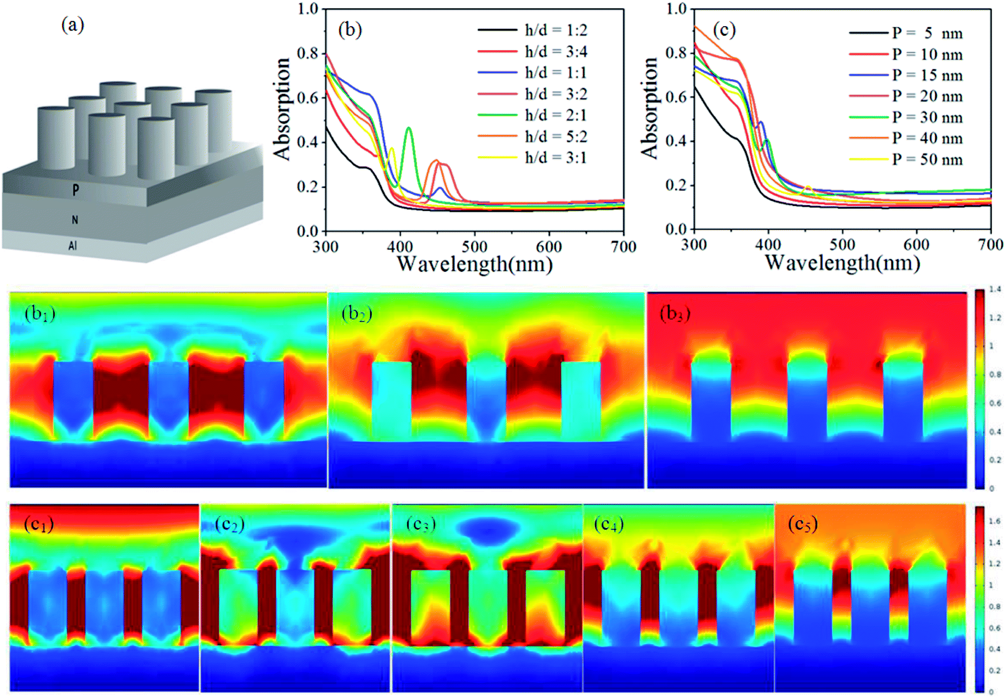 | ||
| Fig. 7 (a) Diagram of the silicon nanopillar solar cell; (b) and (c) absorption with the wavelength range of 300–700 nm based on different high aspect ratios or periodicities for silicon nanopillar solar cells. The distribution of electric field intensity for this structure (h/d = 2:1) is also illustrated in (b1–b3) with the incident wavelengths of λ = 300, 455, and 700 nm, respectively. The distribution of electric field intensity for this structure (P = 20 nm) is illustrated in (c1–c5) with the incident wavelengths λ = 300, 380, 390, 500, and 700 nm. | ||
In addition, Fig. 8(a and b) illustrates the absorption spectra of the silicon nanopillar solar cells with different thicknesses of silicon nitride (L = 4, 9, 20, 30, and 40 nm). In Fig. 8(a), the silicon nanopillar solar cell uses a thin silicon nitride coating to passivate the top surface, usually as an antireflection coating. A high aspect ratio (h/d = 2:1) was applied, and the diameter or periodicity were both 40 nm. In this calculation, the simulation based on the incident light was performed vertically. Due to the varying thickness of silicon nitride, using the optimal parameters for the silicon nanopillar solar cells allowed obtaining the best of light absorption. As observed in Fig. 8(b), the average absorptions of the different thicknesses for silicon nitride (L = 4, 9 and 20 nm) for the radial pillar solar cell with the light wavelength range 300–700 nm were 33.72%, 35.33%, and 37.32%, while the average absorptions for the thickness of silicon nitride of L = 30 and 40 nm were 31.99% and 30.98%, respectively. As inspected, the light absorption for all the different thicknesses of silicon nitride (L = 4, 9, 30, and 40 nm) was less than the light absorption for a thickness of silicon nitride of L = 20 nm for the nanopillar solar cell. Furthermore, Fig. 8(b) illustrates the absorption spectra of the silicon nanopillar solar cell structure without silicon nitride. Therefore, by comparing the absorption of the two models, the ability to absorb light of combined model was better than that for the model without an antireflection coating. Fig. 8(b1–b5) illustrate the distribution of electric field intensity for this structure with the different thicknesses of L = 4, 9, 20, 30, and 40 nm of silicon nitride with the incident wavelength of 350 nm. As well as the optimal light-trapping structure of the silicon nanopillar solar cell, this structure also causes a strong field enhancement between the silicon nitride and the surface active layer. So the absorption of the surface film of silicon nanopillar solar cell is also enhanced by the antireflection-coating structure.
 | ||
| Fig. 8 (a) Diagram of the silicon combined (nanopillar with silicon nitride) solar cell; (b) absorption with the wavelength range of 300–700 nm based on different thicknesses of silicon nitride silicon nanopillar solar cell. The distribution of electric field intensity for this structure with the silicon nitride is also illustrated in (b1–b5) with the incident wavelength of λ = 350 nm. | ||
Panels (a–c) of Fig. 9 show SEM micrographs of silicon nanopillar arrays with different high aspect ratios. As can be seen in Fig. 9(a and b), the surface or cross-sectional SEM images of the nanopillar arrays with the scale of 10 μm show that the thickness of the positive photoresist is 971.4 nm, and the diameter of nanopillar is from 4.66 μm to 5.10 μm. In the experiment, the exposed silicon dioxide of the samples was etched in a solution of NH4F, HF, and deionized water with the ratio 6 g:3 ml:10 ml for 45 s at room temperature (see Fig. 1(c3)). The edge of silicon dioxide was etched. The edge of the 5 μm circular pattern positive photoresist point was etched by the plasma of SF6 and O2 with the increasing etching time. Then, the exposed silicon surface without silicon dioxide was etched. As shown in Fig. 9(c), the experimental results show that the morphologies of the silicon nanopillar arrays were deposited on the silicon surface when the circular-shape positive photoresist points were cleaned by the acetone solution. Also, a better shape of nanopillar arrays was obtained with the high aspect ratio (h/d = 2:1). Fig. 9(d) presents the total reflections of the silicon nanopillar solar cells with different high aspect ratios of nanopillar arrays. The average reflections of the high aspect ratios (h/d = 1:2, 3:2, and 2:1) for the nanopillar cell in the range of 300–1100 nm are 27.9%, 23.59%, and 17.76%, while the average reflection of the silicon planar was 43.44%. The high aspect ratio (h/d = 2:1) of the silicon nanopillar solar cell with a lower reflectance would trap more incident light.
 | ||
| Fig. 9 (a)–(c) SEM micrographs of silicon nanopillar arrays with the different high aspect ratios (d) total reflections of the different high aspect ratios for the silicon nanopillar solar cells. | ||
3.5 Electrical characteristics of the silicon nanopillar solar cell with silicon nitride
Fig. 10(a) presents the total reflections of silicon nitride films on the glasses with different deposition times by plasma-enhanced chemical vapor deposition. The average reflection of the deposition times t = 4, 6, and 8 min for the silicon nitride films in the range of 300–1000 nm were 21.53%, 23.17%, and 26.26%, while the average reflection for the deposition times t = 10, 12, and 14 min were 21.25%, 26%, and 30.35%. As inspected, the light reflections of t = 4, 6, 8, 12, or 14 min were more than that for t = 10 min in this film of structures. As a result, to reflect the incident light, with the increase in deposition time, the reflection efficiency is increased first and then decreases, and the film with a deposition time of t = 10 min had the lowest of reflection. The silicon nanopillar solar cell with a lower reflection would trap incident light more than the higher reflection cells. So the deposition time t = 10 min of silicon nitride films was applied for the silicon nanopillar solar cell as the antireflection coating. So the silicon nanopillar solar cell with h/d = 2:1 and a deposition time of t = 10 min of silicon nitride films was applied on the combined structure (silicon nanopillar/silicon nitride solar cells). Fig. 10(b) presents the total reflections of the combined structure and an untreated structure. The average reflections of the two kinds of solar cells in the range of 300–1100 nm were 13.77% and 17.76%. The combined solar cell with a lower reflectance would trap more incident light.
 | ||
| Fig. 10 (a) Total reflections of the different depositing times for the silicon nitride films. (b) Total reflections of the silicon nanopillar/silicon nitride solar cells and of the untreated structure. | ||
Four kinds of solar cells based on different structures were measured under AM 1.5G illumination, as shown in the current density–voltage (J–V) characterization in Fig. 11 and Table 1. Table 1 shows the results of the J–V measurements of silicon planar, nanocone, nanopillar, and combined solar cells under the standard test conditions. The three kinds of solar cells with a lower reflection trap the incident light more than the higher reflection of cells. Therefore, the etching time t = 30 min for the silicon nanowire solar cell, the ICP etching time t = 3 min for the silicon nanocone solar cell, and the high aspect ratio h/d = 2:1 were applied.
 | ||
| Fig. 11 J–V characteristics of four kinds of silicon (planar, nanowire, nanocone, nanopillar) heterojunction solar cell. | ||
| JSC (mA cm−2) | VOC (V) | FF (%) | PCE (%) | |
|---|---|---|---|---|
| Si planar solar cell | 22.5 | 0.360 | 62 | 5.02 |
| Nanowire/30 min | 24.9 | 0.382 | 60 | 5.76 |
| Nanocone/3 min | 25.3 | 0.544 | 55 | 7.62 |
| Nanopillar/(h/d = 2:1) |
25.5 | 0.580 | 57 | 8.40 |
| Nanopillar with silicon nitride | 28.8 | 0.574 | 58 | 9.40 |
The power conversion efficiency of the solar cell is η:
 | (3) |
 is related to the light absorption and carrier collection.
The maximum current density JSC of the four kinds of cells appears in nanopillars/(h/d = 2:1), in which the mean value of JSC was higher than for planar, nanowires/30 min or nanocones/3 min by 3, 0.6, and 0.2 mA cm−2. But the mean value of JSC for nanopillars with silicon nitride is higher than for nanopillars/(h/d = 2:1) by 3.3 mA cm−2 and more than for planar and nanowires/30 min or nanocones/3 min by 6.3, 3.9, and 3.5 mA cm−2. Moreover, it could be observed that the PCE values of the silicon wires/nanocones/pillars solar cell were 5.76%, 7.62%, and 8.40%, while that of the silicon planar solar cell was 5.02%. Thus, there was a significant increase in the photovoltaic performance from such nanostructures to the planar structure.
In addition, it could be observed that the JSC of the solar cell with the nanopillar/(h/d = 2:1) was 25.5 mA cm−2, while that of the combined structure with (nanopillar with silicon nitride) was 28.8 mA cm−2. Thus, there was a significant increase for light wavelengths from the combined solar cell to the untreated structure. On the other hand, the performance of the combined solar cell was better than that of the untreated solar cell. This was in accordance with the markedly higher light absorbed and lower reflection by the structure, as shown in Fig. 8(a) and 10(a). It can be seen that the combined structure (nanopillar with silicon nitride) exhibited a PCE of 9.4% (JSC = 28.8 mA cm−2, VOC = 574 mV, FF = 58%). In contrast, one fabricated on the untreated structure (nanopillar/h/d = 2:1) had a PCE of 8.4% (JSC = 25.5 mA cm−2, VOC = 580 mV, FF = 57%). The properties of trapping light for silicon nitride films have a prominent impact on the improvement of the power conversion efficiency for the hybrid solar cells. Also, the nanowire and nanocone structures exhibited a lower PCE of 5.76% (JSC = 24.9 mA cm−2, VOC = 382 mV, FF = 60%) and 7.62% (JSC = 25.3 mA cm−2, VOC = 544 mV, FF = 55%). Compared to the silicon nanowire or nanocone solar cells, the light trapping of the silicon nanopillar solar cell is low, although the performance is not disappointing. Also, the PCE of nanopillar/(h/d = 2:1) was enhanced by 31%, while the PCE of combined structure (nanopillar with silicon nitride) was enhanced by 38%, in contrast to the silicon nanowire solar cell, as shown in the set of Table 1. Although the structure with the nanowire/30 min and nanocone/3 min exhibited a better light trapping ability, both the mean values of FF and VOC of the solar cells were similar and lower than that of the cell based on the antireflection coating, as shown in Table 1.
4. Conclusion
In this paper, we introduced the ICP method for preparing two kinds of silicon solar cell arrays: silicon nanocones and silicon nanopillars. Moreover, silicon nanowire arrays were also prepared by a Ag-assisted chemical etching method. We simulated the performance of the silicon planar, nanowire, nanocone, nanopillar, and combined solar cells with the absorption of light for different heights or periodicities of arrays. The optimal percents of light absorption for the silicon wires/nanocones/pillars/combined solar cells were 24.02%, 42.49%, 29.32%, and 37.32%, respectively. By comparing the absorption and the optimal electric field intensity distribution of the combined structure and untreated structure, the ability to absorb light of the combined model was better than the untreated structure. Finally, we experimentally demonstrated the current density–voltage characterization of the four structures. The PCE of the solar cell based on the combined structure was better than that of the nanopillar array. As for the antireflection coating films, silicon nitride was applied for the silicon nanopillar solar cell, and a PCE of 9.4% for the combined solar cell was obtained. This had a prominent impact on the improvement of PCE for silicon nanopillar solar cells.Conflicts of interest
There are no conflicts to declare.References
- J. C. Jimeno, V. Rodríguez, R. Gutiérrez, F. Recart, G. Bueno and F. Hernando, 16th Eur. Photovoltaic Sol. Energy Conf., 2000, vol. 5, pp. 1–5 Search PubMed.
- K. S. Do, T. H. Baek, M. G. Kang, S. J. Choi, G. H. Kang, G. J. Yu, J. C. Lee, J. M. Myoung and H. E. Song, Met. Mater. Int., 2014, 20, 545–550 CrossRef CAS.
- X. Li, Y. Xiao, K. Zhou, J. Wang, S. L. Schweizer, A. Sprafke, J.-H. Lee and R. B. Wehrspohn, Phys. Chem. Chem. Phys., 2015, 17, 800–804 RSC.
- S. Y. Zhang, W. Liu, Z. F. Li, M. Liu, Y. S. Liu, X. D. Wang and F. H. Yang, Chin. Phys. B, 2016, 25, 106802 CrossRef.
- L. H. Niu, X. H. Jiang, Y. L. Zhao, H. G. Ma, J. J. Yang, K. Cheng and Z. L. Du, Nanotechnology, 2016, 27, 315601 CrossRef PubMed.
- Z. Fan, W. Zhang, Y. Fu, L. Yan and X. Ma, J. Phys. Chem. C, 2016, 120, 6824–6834 CrossRef CAS.
- Y. He, J. Quan and G. Ouyang, Phys. Chem. Chem. Phys., 2016, 18, 7001–7006 RSC.
- Y. P. Xing, K. L. Zhang, J. S. Zhao, P. D. Han, Z. C. Yang, Y. J. Yuan and Q. Ding, Optik, 2017, 128, 133–138 CrossRef CAS.
- D. R. Kim, C. H. Lee, P. M. Rao, I. S. Cho and X. Zheng, Nano Lett., 2011, 11, 2704–2708 CrossRef CAS PubMed.
- B. Dou, R. Jia, H. Li, C. Chen, W. Ding, Y. Meng, Z. Xing, X. Liu and T. Ye, Appl. Phys. Lett., 2012, 101(18), 183901 CrossRef.
- J. Shieh, Y. C. Li, C. Y. Ji, C. C. Chiu and H. Y. Lin, J. Renewable Sustainable Energy, 2015, 7, 033102 CrossRef.
- J. Zhu, Z. F. Yu, G. F. Burkhard, C. M. Hsu, S. T. Connor, Y. Q. Xu, Q. Wang, M. McGehee, S. H. Fan and Y. Cui, Nano Lett., 2009, 9, 279–282 CrossRef CAS PubMed.
- H. F. Li, R. Jia, C. Chen, Z. Xing, W. C. Ding, Y. L. Meng, D. Q. Wu, X. Y. Liu and T. C. Ye, Appl. Phys. Lett., 2011, 98, 151116 CrossRef.
- M. D. Kelzenberg, S. W. Boettcher, J. A. Petykiewicz, D. B. Turner-Evans, M. C. Putnam, E. L. Warren, J. M. Spurgeon, R. M. Briggs, N. S. Lewis and H. A. Atwater, Nat. Mater., 2010, 9, 239–244 CrossRef CAS PubMed.
- G. Andra, M. Pietsch, T. Stelzner, A. Gawlik, E. Ose, S. Christiansen, F. Falk and IEEE, in Pvsc: 2008 33rd IEEE Photovoltaic Spec. Conf., 2008, vol. 1–4, pp. 118–121 Search PubMed.
- A. Surawijaya, I. Anshori, A. Rohiman and I. Idris, 4th Nanosci. Nanotechnol. Symposi., ed. F. Iskandar, Khairurrijal and M. Abdullah, 2011, p. 1415 Search PubMed.
- M. F. Hainey and J. M. Redwing, Appl. Phys. Rev., 2016, 3, 040806 Search PubMed.
- H. Fang, Y. Wu, J. H. Zhao and J. Zhu, Nanotechnology, 2006, 17, 3768–3774 CrossRef CAS.
- M.-L. Zhang, K.-Q. Peng, X. Fan, J.-S. Jie, R.-Q. Zhang, S.-T. Lee and N.-B. Wong, J. Phys. Chem. C, 2008, 112, 4444–4450 CrossRef CAS.
- K. Q. Peng, J. J. Hu, Y. J. Yan, Y. Wu, H. Fang, Y. Xu, S. T. Lee and J. Zhu, Adv. Funct. Mater., 2006, 16, 387–394 CrossRef CAS.
- K. Pal, U. N. Maiti, T. P. Majumder, P. Dash, N. C. Mishra, N. Bennis and J. M. Otón, J. Mol. Liq., 2011, 164, 233–238 CrossRef CAS.
- S. Sagadevan, K. Pal and Z. Z. Chowdhury, J. Mater. Sci.: Mater. Electron., 2017, 28(22), 17193–17201 CrossRef CAS.
- K. Pal, T. P. Majumder, C. Neogy and S. C. Debnath, J. Mol. Struct., 2012, 1016, 30–38 CrossRef CAS.
- H. J. Syu, S. C. Shiu and C. F. Lin, Sol. Energy Mater. Sol. Cells, 2012, 98, 267–272 CrossRef CAS.
- Z. W. Zuo, K. Zhu, G. L. Cui, W. X. Huang, J. Qu, Y. Shi, Y. S. Liu and G. B. Ji, Sol. Energy Mater. Sol. Cells, 2014, 125, 248–252 CrossRef CAS.
- A. Najar, A. B. Slimane, M. N. Hedhili, D. Anjum, R. Sougrat, T. K. Ng and B. S. Ooi, J. Appl. Phys., 2012, 112, 033502 CrossRef.
- H. Chen, Q. Zhang and S. Y. Chou, Nanotechnology, 2015, 26, 085302 CrossRef CAS PubMed.
- J. Liu, X. S. Zhang, G. J. Sun, Y. T. Wang, B. Wang, T. C. Zhang, F. T. Yi and F. Chen, Energy Technol., 2016, 4, 298–303 CrossRef CAS.
- J. Liu, Y. X. Liao, B. Wang and F. T. Yi, Sol. Energy, 2011, 694, 375–379 CAS.
- A. Pateau, A. Rhallabi, M. C. Fernandez, M. Boufnichel and F. Roqueta, J. Vac. Sci. Technol., A, 2014, 32(2), 021303 CrossRef.
- S. C. Chen, Y. C. Lin, J. C. Wu, L. Horng and C. H. Cheng, Microsyst. Technol., 2007, 13, 465–474 CrossRef CAS.
- H. Tosaka US Pat. Appl., A1[P], US20080299777, 2008.
- E. Garnett and P. Yang, Nano Lett., 2010, 10, 1082–1087 CrossRef CAS PubMed.
- L. S. Golobokova, Y. V. Nastaushev, F. N. Dultsev, D. V. Gulyaev, A. B. Talochkin and A. V. Latyshev, in Iop 1st Inter. Sch. Conf., S-Peters, 2014, p. 541 Search PubMed.
- L. Tsakalakos, J. Balch, J. Fronheiser, B. A. Korevaar, O. Sulima and J. Rand, Appl. Phys. Lett., 2007, 91, 233117 CrossRef.
- L. Tsakalakos, J. Balch, J. Fronheiser, M. Y. Shih, S. F. LeBoeuf, M. Pietrzykowski, P. J. Codella, O. Sulima, J. Rand, A. D. Kumar, B. A. Korevaar and IEEE, W. Conf. on Photovol. Energy Conf., 2006, pp. 111–113 Search PubMed.
- L. Hu and G. Chen, Nano Lett., 2007, 7, 3249–3252 CrossRef CAS PubMed.
- Q. T. Li, Z. C. Ni, S. M. Yang, J. L. Gong, D. Z. Zhu and Z. Y. Zhu, Nucl. Instrum. Methods Phys. Res., 2008, 266, 197–202 CrossRef CAS.
- X. M. Meng, N. G. Shang, C. S. Lee, I. Bello and S. T. Lee, Phys. Status Solidi A, 2005, 202, 2479–2483 CrossRef CAS.
- K. C. Sahoo, M. K. Lin, E. Y. Chang, T. B. Tinh, Y. M. Li and J. H. Huang, Jpn. J. Appl. Phys., 2009, 48, 126508 CrossRef.
- H. P. Wang, K. Y. Lai, Y. R. Lin, C. A. Lin and J. H. He, Langmuir, 2010, 26, 12855–12858 CrossRef CAS PubMed.
- P. F. Liu, P. Gemeiner, H. Shen, X. J. Meng, J. H. Chu, S. Geiger, N. Guiblin and B. Dkhil, J. Appl. Phys., 2009, 106, 054111 CrossRef.
- G. Conibeer, M. Green, R. Corkish, Y. Cho, E. C. Cho, C. W. Jiang, T. Fangsuwannarak, E. Pink, Y. Huang, T. Puzzer, T. Trupke, B. Richards, A. Shalav and K. L. Lin, Thin Solid Films, 2006, 511–512, 654–662 CrossRef CAS.
- J. S. Li, H. Y. Yu, S. M. Wong, G. Zhang, X. W. Sun, P. G. Q. Lo and D. L. Kwong, Appl. Phys. Lett., 2009, 95, 255101 Search PubMed.
- H. Shen, P. Bienstman and B. Maes, J. Appl. Phys., 2009, 106, 073109 CrossRef.
- Y.-K. Jia, E. Yang Shi, Q.-N. Guo, Y.-S. Chen, X.-Y. Gao, J.-H. Gu and J.-X. Lu, Acta Phys. Sin., 2013, 62, 247801 Search PubMed.
- F. Shan, T. Zhang and S.-Q. Zhu, J. Nanomater., 2014, 827658 Search PubMed.
- X. Li, N. P. Hylton, V. Giannini, K.-H. Lee, N. J. Ekins-Daukes and S. A. Maier, Opt. Express, 2011, 19, A888–A896 CrossRef CAS PubMed.
Footnote |
| † These authors contribute equally. |
| This journal is © The Royal Society of Chemistry 2018 |