
 Open Access Article
 This Open Access Article is licensed under a Creative Commons Attribution-Non Commercial 3.0 Unported Licence
Facile tailoring of the electrical transport in representative hole transport materials by molecular doping†
Bixin Li *a,
Chenyang Zhaob,
Shiyang Zhanga and
Min Zhena
*a,
Chenyang Zhaob,
Shiyang Zhanga and
Min Zhena
aDepartment of Science Education, Laboratory of College Physics, Hunan First Normal University, Changsha 410205, People’s Republic of China. E-mail: lbxin86@hotmail.com
bState Key Laboratory of Polymer Physics and Chemistry, Changchun Institute of Applied Chemistry, University of Chinese Academy of Sciences, Changchun 130022, People’s Republic of China
First published on 23rd July 2018
Abstract
N,N′-Diphenyl-N,N′-bis(1-naphthyl)-1,1′-biphenyl-4,4′-diamine (NPB) and 4,4′,4′′-tris (N-3-methylphenyl-N-phenylamine) triphenylamine (m-MTDATA) are widely used as hole transport materials in organic optoelectronic devices. In the present article, the hole transport properties of blends of NPB and m-MTDATA compared with the pristine materials are investigated using admittance spectroscopy and considering temperature dependent current–voltage characteristics and electroluminescent characteristics. It has been found that m-MTDATA dramatically lowers the carrier mobility in the NPB matrix to a large extent by enhancing the total density of traps and results in more dispersive transport. However, by introducing NPB into m-MTDATA the hole mobility is nearly unchanged in comparison with pristine m-MTDATA film. These differences are attributed to two different charge transport mechanisms, trapping and scattering. Obtained quantitative information regarding the charge transport parameters could help to extend optimization strategies for the fabrication of new organic optoelectronic devices by enabling the facile tailoring of the charge transport process.
1. Introduction
Organic doped semiconductors have invoked immense interest as active layers in next generation optoelectronic devices, such as organic light emitting diodes (OLEDs),1 organic solar cells (OSCs)2 and organic thin film transistors (OTFTs).3 The efficiency of OLEDs is governed by engineering the charge transport properties of organic semiconductors to achieve a charge balance between electrons and holes in charge transport layers.4 Electrical doping is an important and feasible method in the recent impressive progress in the performance of organic semiconducting devices. However few efforts are focused on the fundamental aspects of this issue.5–11 Understanding the charge transport properties in organic doped films and the related diode characteristics is therefore of great significance for the further improvement of device efficiency.The role that the dopant plays in the doped film is crucial in the transport process. Doping of a hole transport material with a dopant with a higher-lying highest occupied molecular orbital (HOMO) level results in an electronic state above the HOMO level of the matrix material while doping with a dopant with a lower-lying HOMO level generates no additional trap states.12–14 These two types of dopant are defined as trap and scatterer, respectively. Subsequently, the influence of charge trapping and scattering on the hole transport properties of N,N′-di(naphthalene-1-yl)-N,N′-diphenyl-benzidine (NPB) has been studied by So et al. via the time-of-flight (TOF) technique.15,16 The charge transport properties were analyzed using the Gaussian disorder model and they revealed that the traps significantly enhance the energetic disorder. For the scattering, it changes a little. The effects of traps and scatterers with various energy level differences have also been investigated.17 In these studies, the mobilities were determined using the TOF technique which generally requires several micron thick films due to the finite penetration depth of the incident light when retaining a well-defined flight distance.18 In particular, the TOF transients become featureless and the carrier transit time is difficult to determine in highly dispersive materials.19 Alternatively, admittance spectroscopy (AS) is a powerful technique for investigating the hole and electron mobilities in organic materials with the advantages of full automatic measurements and no specific requirements for the sample thickness.5,9,10,19–25 It is superior to TOF for investigating the charge transport in dispersive materials. Furthermore, the space-charge-limited current (SCLC) model with exponentially distributed traps is commonly used to describe the current–voltage (I–V) characteristics in organic disordered semiconductors with an estimation of the energy and density of traps.26,27 So how the trap densities are influenced upon doping will be revealed.
In the present work, we investigate the effects of intentional doping on NPB and 4,4′,4′′-tris(N-3-methylphenyl-N-phenylamine) triphenylamine (m-MTDATA) by considering I–V and capacitance–frequency (C–f) characteristics. In NPB-doped m-MTDATA and m-MTDATA-doped NPB films, the mobilities and dispersion parameters as well as trap densities are determined and compared with those of pristine materials. These obtained physical quantities show that the transport properties can be tailored facilely.
2. Experimental
NPB and m-MTDATA were chosen for this investigation. The HOMO levels of m-MTDATA and NPB are 5.1 eV and 5.4 eV, respectively. Therefore, the introduction of hole traps is expected when doping m-MTDATA into NPB, while NPB would behave as scattering centers in an m-MTDATA matrix.13,15 All organic materials were purchased from Nichem and used without further purification.The devices were fabricated by thermal evaporation of the organic materials on indium tin oxide (ITO)-coated glass substrates. The substrate was thoroughly cleaned in an ultrasonic bath using detergents and then de-ionized water. The surface of the ITO substrate was treated with oxygen plasma for 2 min to enhance its work function. All films were deposited under a high vacuum (pressure <10−4 Pa). The doped films were deposited using a co-evaporation process with a doping concentration of 4% by weight. The thickness was controlled in situ using a quarter crystal monitor and calibrated using a Dektak 6M Profiler (Veeco). The aluminum (Al) electrodes were deposited on the organic films through shadow masks with an active area of 16 mm2.
For the measurements of the temperature dependent I–V characteristics, the device structure is ITO/molybdenum oxide (MoO3) (5 nm)/active layers (120 nm)/MoO3 (5 nm)/Al, where MoO3 was used to facilitate hole injection from ITO and suppress electron injection from Al.5 For the AS measurements, the samples had the same structure as mentioned above but the thicknesses were between 120 and 1400 nm to efficiently derive mobilities in different samples due to the limitation of the maximum frequency in the impedance analyzer.
The I–V characteristics were investigated using a Keithley 2400 sourcemeter integrated with a vacuum cryostat (Optistat DN-V, Oxford Instruments). The admittance was measured at room temperature using an Agilent E4980A precision LCR meter in the frequency range of 20 Hz to 2 MHz with the oscillation amplitude of the ac voltage kept at 100 mV. The luminance–voltage (L–V) characteristics were recorded using a Keithley 2400 sourcemeter and a Keithley 2000 multimeter with a calibrated silicon photodiode.
3. Results and discussion
Fig. 1 shows the current density–voltage (J–V) characteristics of the hole-only devices for pure and doped films at room temperature. It can be clearly seen that for a given driving voltage the current density decreases around three or four orders of magnitude when m-MTDATA is doped into NPB. In particular, the device based on m-MTDATA:NPB exhibits slightly reduced, or nearly identical, J–V characteristics compared with those of pristine m-MTDATA. For example, at a voltage of 3 V, the current density is 0.034 A cm−2 for pure NPB, which reduces sharply to 3.2 × 10⁻⁶ A cm−2 in m-MTDATA doped NPB film. Meanwhile, the current densities of pristine m-MTDATA and NPB doped m-MTDATA films are 0.0064 A cm−2 and 0.0055 A cm−2, respectively. The variations in the J–V characteristics implies the different mobilities in doped films, which are related to the charge transport hopping process via the dopant molecules.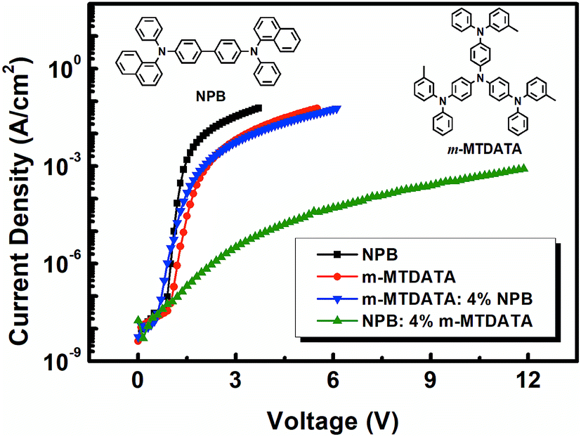 | ||
| Fig. 1 Current density–voltage characteristics of the hole-only devices. The chemical structures of NPB and m-MTDATA are also shown here. | ||
AS measurements were done to infer the hole transport properties based on the measurement of the frequency-dependent capacitance of an organic film. In this method, the current response, iac, to a small oscillating voltage, vac, is monitored. The complex admittance, Yac, is related to iac and vac as follows:
 | (1) |
 | (2) |
![[small mu, Greek, tilde]](https://www.rsc.org/images/entities/i_char_e0e0.gif) (Ω) = μ(Ω)/μdc, where μdc = d2/(Vτdc) is the dc hole mobility in the absence of the ac field. To derive the carrier mobility, the imaginary part of Y, i.e. the susceptance in the frequency domain, can be analyzed. In particular, the negative differential susceptance of the device can be defined as −ΔB = −2πf(C − Cgeo). By plotting −ΔB as a function of frequency, a characteristic frequency fr at which a maximum of −ΔB occurs is correlated with the average hole transit time via fr = 0.56/τdc.20 Consequently the carrier mobility can be extracted by the following equation:
(Ω) = μ(Ω)/μdc, where μdc = d2/(Vτdc) is the dc hole mobility in the absence of the ac field. To derive the carrier mobility, the imaginary part of Y, i.e. the susceptance in the frequency domain, can be analyzed. In particular, the negative differential susceptance of the device can be defined as −ΔB = −2πf(C − Cgeo). By plotting −ΔB as a function of frequency, a characteristic frequency fr at which a maximum of −ΔB occurs is correlated with the average hole transit time via fr = 0.56/τdc.20 Consequently the carrier mobility can be extracted by the following equation:
 | (3) |
Fig. 2 depicts a series of corresponding C–f and −ΔB–f plots for four devices. It can be observed that at zero bias voltage, the capacitances are nearly frequency independent and equal to the geometrical capacitance. As bias increases, the capacitance becomes frequency dependent. Due to hole trapping, the excess capacitance can be observed at lower frequencies. With increasing frequencies, a clear valley-like response appears in each C–f curve. Each device shows a minimum capacitance in the intermediate frequency region and then the capacitances tend to their respective geometrical capacitances at high frequency. By replotting the data as −ΔB versus frequency, the peak fr can be clearly observed. The shift of fr to higher frequencies with increasing voltage indicates the field dependence of the mobility.
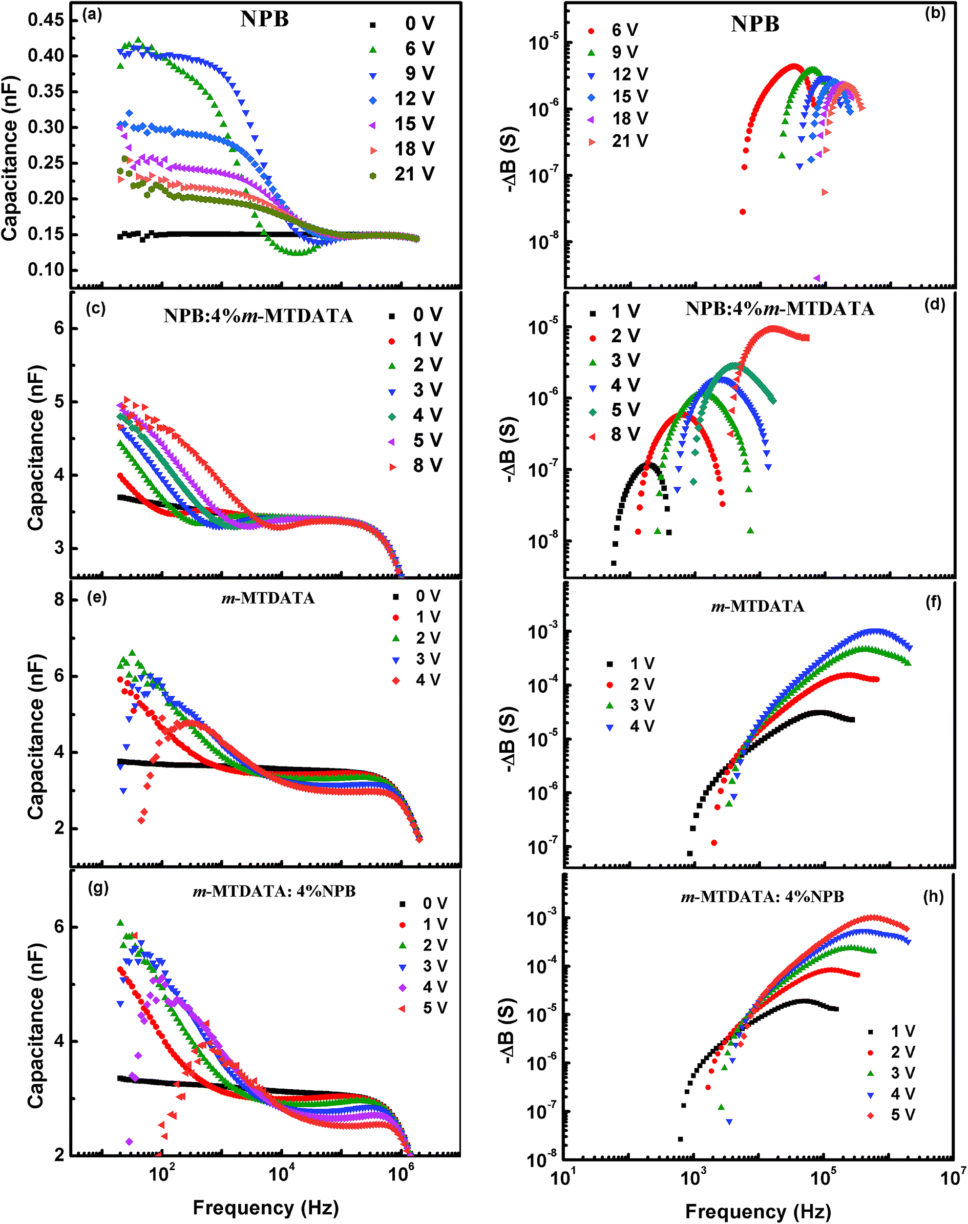 | ||
| Fig. 2 Frequency dependences of capacitance and −ΔB for hole-only devices of (a and b) NPB, (c and d) NPB:4% m-MTDATA, (e and f) m-MTDATA, (g and h) m-MTDATA:4% NPB at room temperature. | ||
Fig. 3 shows the mobilities derived from fr using eqn (3). It can be clearly seen that the mobilities follow the Poole–Frenkel dependence.28 The hole mobilities for the pristine NPB and m-MTDATA film are in the ranges of (2–4) × 10−4 cm2 V−1 s−1 and (2–4) × 10−5 cm2 V−1 s−1, respectively. In the case of m-MTDATA-doped NPB, the hole mobility reduces dramatically by four orders of magnitude. Meanwhile, for m-MTDATA doped with NPB, there is only a slight reduction in mobility or the values are nearly the same. This phenomenon suggests that traps and scatterers have different effects on hole transport mechanisms.15,16 In the case of trapping, the mobile holes may be trapped in the generated trap level and then de-trapped by thermal energy. These processes will lead to a reduction in the mobility due to the additional trap residing time. In the case of scattering, the holes may be hampered by the dopant with a lower-lying HOMO level due to collisions. However, holes may transport nearly unrestrainedly in the film.
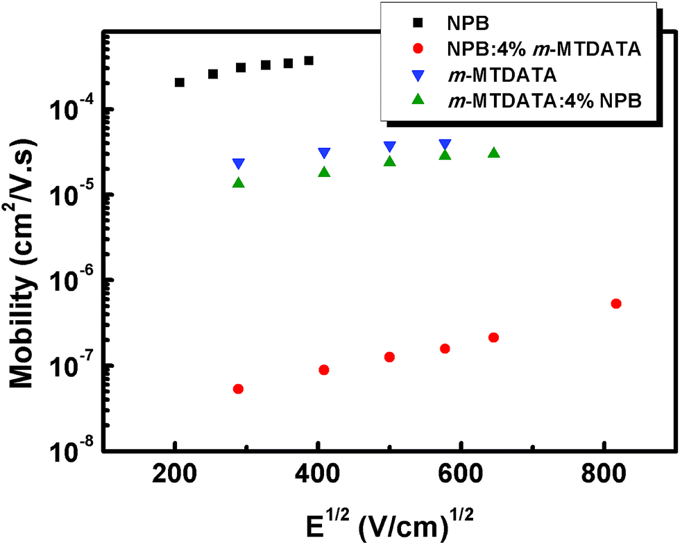 | ||
| Fig. 3 Field dependent hole mobilities of NPB, NPB:m-MTDATA, m-MTDATA and m-MTDATA:NPB at room temperature. | ||
The immobilization of carriers for time periods by trapping sites that are distributed in energy gap leads to a broad distribution of transit times, rendering the transport more dispersive. It has been shown that in a multiple trapping model, the transit time of the carriers exhibits an electric field dependence of τtr(E) ∝ E−1/α, where α is a dispersion parameter (0 < α < 1, α = 1 for non-dispersive transport) that describes dispersive transport in amorphous solids.29 Generally, a more dispersive charge transport would result in a smaller value of α. In addition, α is related to the expression α = T/Tt, where Tt is the characteristic temperature of trap distribution. The electric field dependence of the hole transit times derived from AS measurements are shown in Fig. 4. From the slope of the line representing the linear fit to the experimental data, the values of α and Tt obtained for different films are summarized in Table 1. It can be clearly seen that the α value of the NPB:4% m-MTDATA based device is the smallest, which suggests that the distribution of trap states in NPB:4% m-MTDATA is the broadest. This result gives direct evidence of the trapping center that m-MTDATA acts as when doped into NPB.
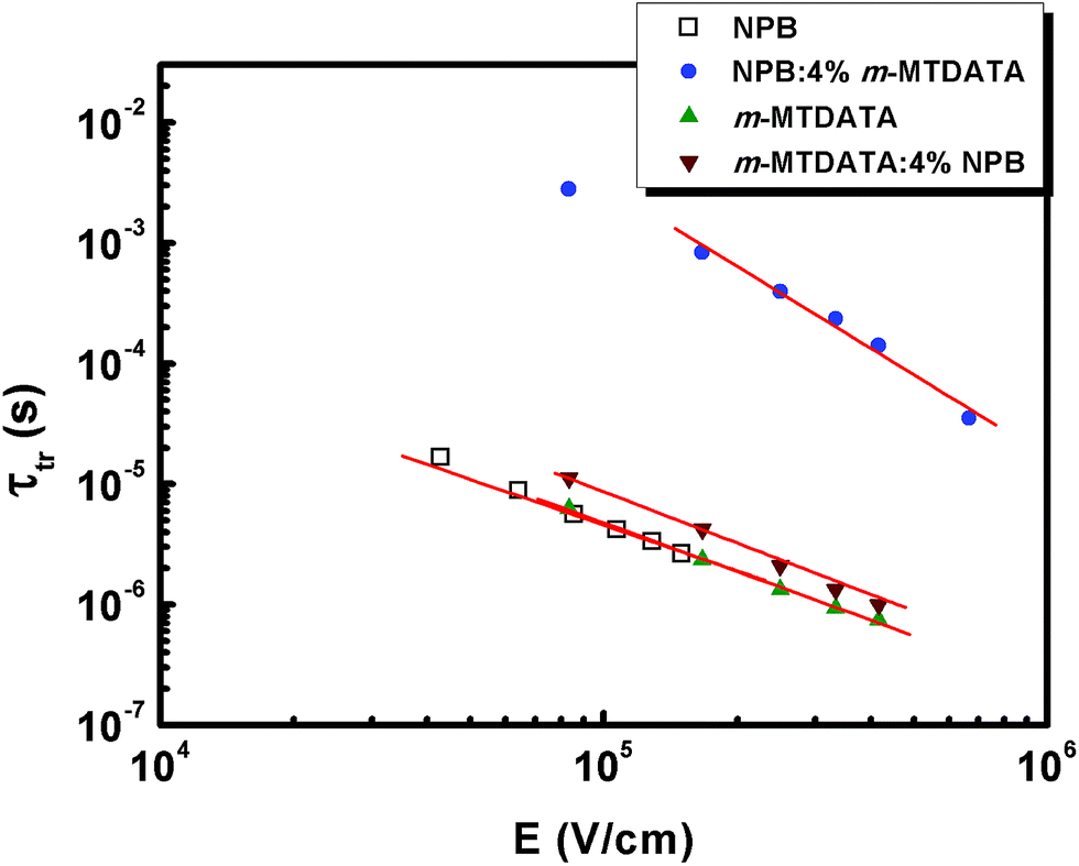 | ||
| Fig. 4 Field dependence of hole transit times. The solid lines represent the linear fits to the data. | ||
| α | Tt (K) | Vc (V) | Nt (cm−3) | |
|---|---|---|---|---|
| NPB | 0.79 | 379 | 11 | 2.5 × 10¹⁷ |
| NPB:4% m-MTDATA | 0.44 | 681 | 103 | 2.4 × 10¹⁸ |
| m-MTDATA | 0.75 | 400 | 50 | 1.2 × 10¹⁸ |
| m-MTDATA:4% NPB | 0.71 | 422 | 78 | 1.8 × 10¹⁸ |
Moreover, the dispersive hole transport can be certified by a C/Cgeo–f/fr plot as shown in Fig. 5. For the NPB:4% m-MTDATA film, the curves for different bias voltages all have the same shape which again reflects the dispersive properties of hole transport.30 However, for the other films, the curves at different bias voltages have different shapes, indicating non-dispersive transport, which is in agreement with the results shown in Table 1.
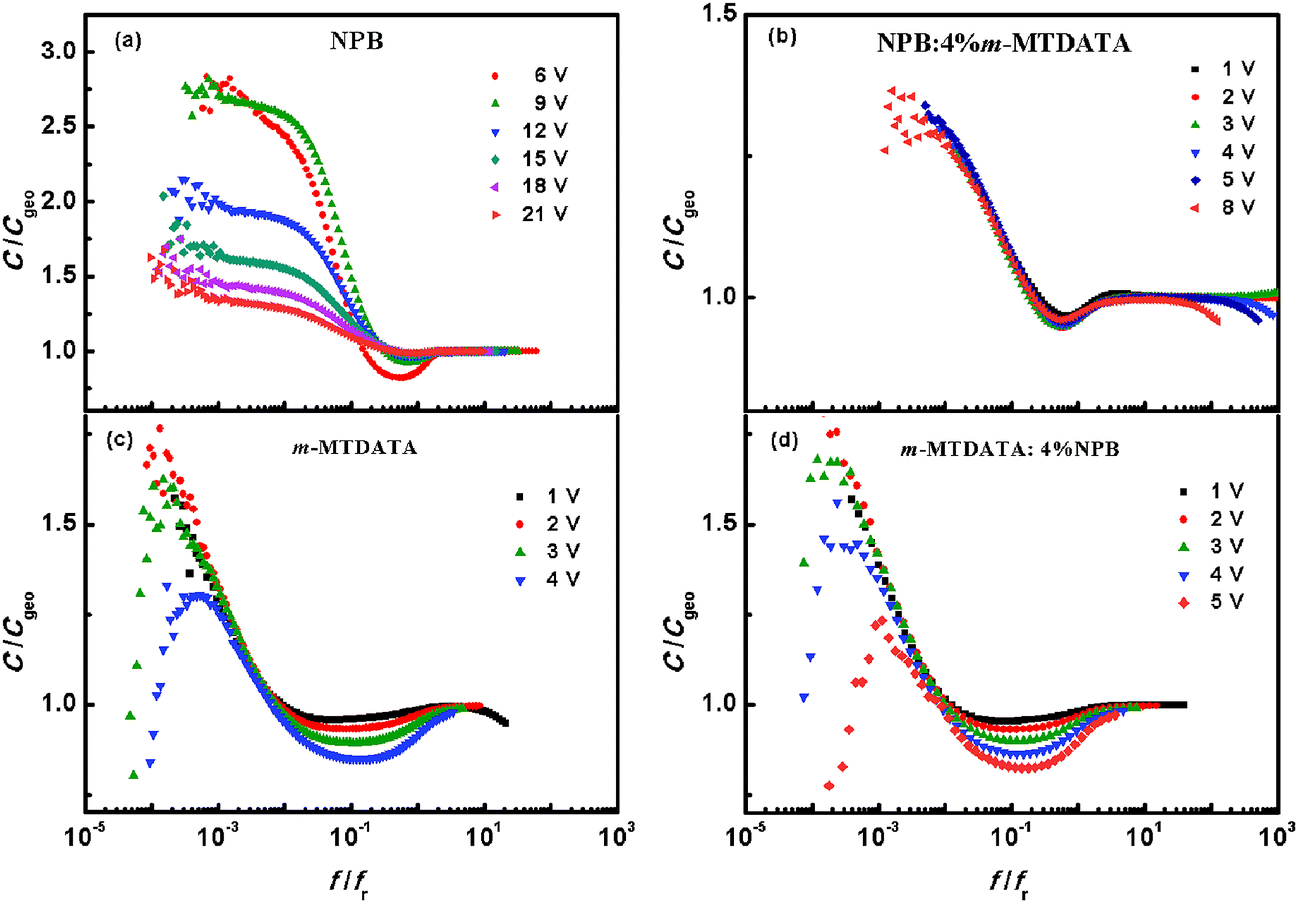 | ||
| Fig. 5 Normalized capacitance C/Cgeo–f/fr curves for (a) NPB, (b) NPB:4% m-MTDATA, (c) m-MTDATA, (d) m-MTDATA:4% NPB. | ||
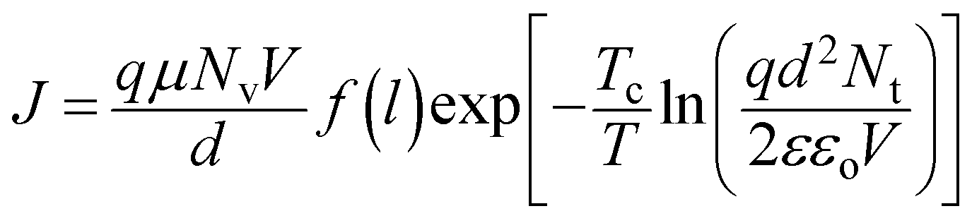
To further distinguish the effect of trapping and scattering on the hole transport properties, the temperature dependent I–V characteristics of different doping devices are shown in Fig. 6. The slopes of the I–V curves on a double logarithmic scale for each device are greater than 2 at room temperature and increase rapidly with decreasing temperature. Hence, the equation for I–V characteristics can be expressed as26
 | (4) |
 | (5) |
 | (6) |
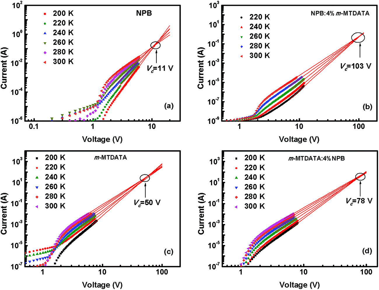 | ||
| Fig. 6 Extrapolation of the I–V curves at different temperatures in log–log scale for (a) NPB, (b) NPB:4% m-MTDATA, (c) m-MTDATA, (d) m-MTDATA:4% NPB hole-only devices. | ||
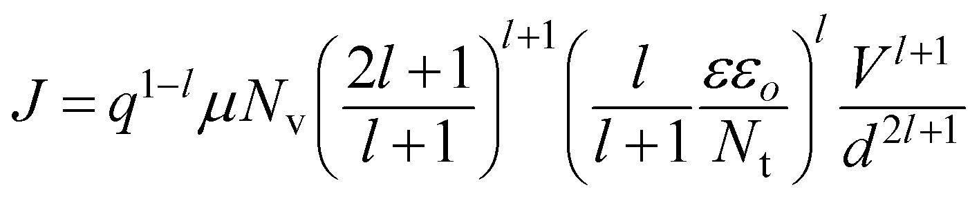
For l > 2, the value of f(l) is about 0.5, so it can be considered as a constant of 0.5. With this approximation, eqn (5) becomes a typical Arrhenius form,
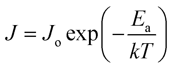 | (7) |
 | (8) |
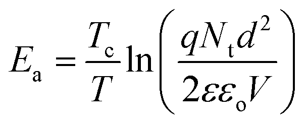
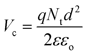
For Ea = 0, J = Jo and current becomes independent of temperature. The I–V curves for different temperatures should then converge at a critical voltage,
 | (9) |
By extrapolating log![[thin space (1/6-em)]](https://www.rsc.org/images/entities/char_2009.gif) I–logV characteristics at various temperatures to higher voltages, Vc can be determined, as shown in Fig. 6. With the obtained Vc and assuming ε = 3, the total density of the traps can be calculated as listed in Table 1.
I–logV characteristics at various temperatures to higher voltages, Vc can be determined, as shown in Fig. 6. With the obtained Vc and assuming ε = 3, the total density of the traps can be calculated as listed in Table 1.
It appears that doping m-MTDATA into NPB raises the total density of traps by one order of magnitude, rendering the distribution of trap states broader. On the contrary, the scatterer NPB has a minimal affect on m-MTDATA with respect to the total density of traps. This result confirms the trapping activity of m-MTDATA in NPB.
Organic films were used as the hole-transporting layers (HTL) to fabricate organic light-emitting diodes with a general configuration of ITO/MoO3 (5 nm)/HTL (60 nm)/NPB (20 nm)/Alq3: 10-(2-benzothiazolyl)-2,3,6,7-tetrahydro-1,1,7,7-tetramethyl-1H,5H,11H-benzo[l]-pyrano-[6,7,8-ij]quinolizin-11-one (C545T) (1%, 30 nm)/Alq3 (30 nm)/LiF (1 nm)/Al or ITO/MoO3 (5 nm)/HTL (60 nm)/m-MTDATA (20 nm)/Alq3: C545T (1%, 30 nm)/Alq3 (30 nm)/LiF (1 nm)/Al for doped NPB and m-MTDATA films, respectively. Inserting a layer of pure NPB or m-MTDATA between the HTL and the emitting layer will block electrons from reaching the HTL and make the interfaces between different HTLs and emitting layers the same. It can be observed from the data shown in Fig. 7 that the current density–voltage (J–V) characteristics for OLEDs with trap doped HTLs differ strongly from those with scatterer doped HTLs. With balanced charge transport in m-MTDATA-doped NPB and Alq3, a maximum efficiency of 24.3 cd A−1 is achieved.32
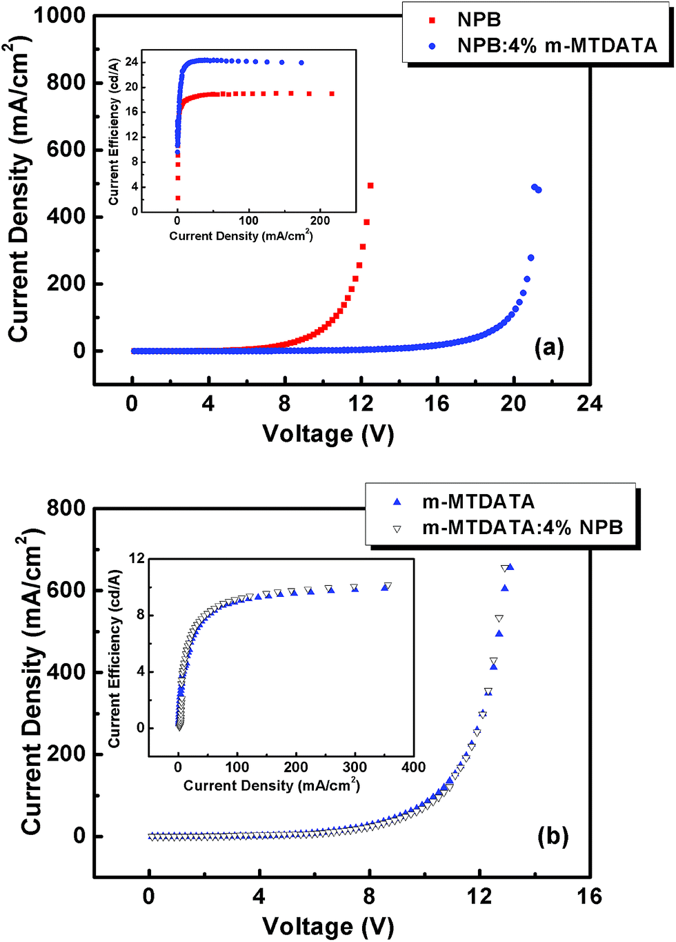 | ||
| Fig. 7 Current density–voltage and current efficiency versus current density characteristics of OLEDs with (a) NPB, NPB:4% m-MTDATA and (b) m-MTDATA, m-MTDATA:4% NPB as the hole transport layer. | ||
4. Conclusions
In conclusion, the hole transport properties of blends of NPB and m-MTDATA compared with the pristine materials were investigated well using admittance spectroscopy and considering temperature dependent current–voltage characteristics and electroluminescent characteristics. The hole transport in NPB:4% m-MTDATA shows more dispersion than that of the other films. The significant differences in trap density, trap distribution and carrier dispersion are responsible for a lowering of the hole mobility in trapping, which is quite distinct from the effect of scattering. These results pave the way for the facile tailoring of the charge transport properties by doping, thus shedding light on improving device performance.Conflicts of interest
There are no conflicts to declare.Acknowledgements
The authors gratefully acknowledge the Scientific Research Fund of Hunan Provincial Education Department (17C0331), the Hunan First Normal University Research Fund (XYS15N01) and the Natural Science Foundation of Hunan Province (Grant No. 2017JJ3046) for their support of this research. The authors also thank Lu She in the Hunan Provincial Tax Service, State Administration of Taxation for the encouragement.References
- C. W. Tang and S. A. Vanslyke, Appl. Phys. Lett., 1987, 51, 913–915 CrossRef.
- C. W. Tang, Appl. Phys. Lett., 1986, 48, 183–185 CrossRef.
- A. Tsumura, H. Koezuka and T. Ando, Appl. Phys. Lett., 1986, 49, 1210–1212 CrossRef.
- Y. Zhang and H. Aziz, Org. Electron., 2016, 30, 76–82 CrossRef.
- M. Hoping, C. Schildknecht, H. Gargouri, T. Riedl, M. Tilgner, H. H. Johannes and W. Kowalsky, Appl. Phys. Lett., 2008, 92, 213306 CrossRef.
- Z. Chiguvare and V. Dyakonov, Phys. Rev. B: Condens. Matter Mater. Phys., 2004, 70, 235207 CrossRef.
- D. Poplavskyy and F. So, J. Appl. Phys., 2006, 99, 033707 CrossRef.
- Y. Yao, H. Dong and W. Hu, Adv. Mater., 2016, 28, 4513–4523 CrossRef PubMed.
- Y. Wang, J. Chen, J. Huang, D. Ma, L. Dong and H. Chen, J. Appl. Phys., 2014, 115, 223707 CrossRef.
- Y. Wang, J. Chen, L. Dong and D. Ma, J. Appl. Phys., 2013, 114, 113703 CrossRef.
- Y. Wang, Q. Liang, J. Huang, D. Ma and Y. Jiao, RSC Adv., 2017, 7, 28494–28498 RSC.
- R. Schmechel and H. von Seggern, Phys. Status Solidi A, 2004, 201, 1215–1235 CrossRef.
- N. von Malm, J. Steiger, R. Schmechel and H. von Seggern, J. Appl. Phys., 2001, 89, 5559–5563 CrossRef.
- S.-W. Liu, J.-H. Lee, C.-C. Lee, C.-T. Chen and J.-K. Wang, Appl. Phys. Lett., 2007, 91, 142106 CrossRef.
- K. K. Tsung and S. K. So, Appl. Phys. Lett., 2008, 92, 103315 CrossRef.
- K. L. Tong, S. W. Tsang, K. K. Tsung, S. C. Tse and S. K. So, J. Appl. Phys., 2007, 102, 093705 CrossRef.
- C. Li, L. Duan, Y. Sun, H. Li and Y. Qiu, J. Phys. Chem. C, 2012, 116, 19748–19754 CrossRef.
- P. M. Borsenberger and D. S. Weiss, Organic Photoreceptors for Imaging Systems, Dekker, New York, 1993 Search PubMed.
- K. K. Tsung and S. K. So, J. Appl. Phys., 2009, 106, 083710 CrossRef.
- S. W. Tsang, S. K. So and J. B. Xu, J. Appl. Phys., 2006, 99, 013706 CrossRef.
- S. W. Tsang, S. C. Tse, K. L. Tong and S. K. So, Org. Electron., 2006, 7, 474–479 CrossRef.
- H. C. F. Martens, H. B. Brom and P. W. M. Blom, Phys. Rev. B: Condens. Matter Mater. Phys., 1999, 60, R8489–R8492 CrossRef.
- H. C. F. Martens, J. N. Huiberts and P. W. M. Blom, Appl. Phys. Lett., 2000, 77, 1852–1854 CrossRef.
- N. Shintaku, S. Izawa, K. Takagi, H. Naito and M. Hiramoto, Org. Electron., 2017, 50, 515–520 CrossRef.
- L. Zhang, H. Nakanotani and C. Adachi, Appl. Phys. Lett., 2013, 103, 093301 CrossRef.
- M. A. Lampert and P. Mark, Current Injection in Solids, Academic New York, 1970 Search PubMed.
- M. R. Khan, P. Anjaneyulu, K. S. R. Koteswara Rao and R. Menon, J. Phys. D: Appl. Phys., 2017, 50, 095103 CrossRef.
- P. N. Murgatroyd, J. Phys. D: Appl. Phys., 1970, 3, 151–156 CrossRef.
- H. Scher and E. W. Montroll, Phys. Rev. B: Solid State, 1975, 12, 2455–2477 CrossRef.
- S. Berleb and W. Brütting, Phys. Rev. Lett., 2002, 89, 286601 CrossRef PubMed.
- V. Kumar, S. C. Jain, A. K. Kapoor, J. Poortmans and R. Mertens, J. Appl. Phys., 2003, 94, 1283–1285 CrossRef.
- S. Barth, P. Müller, H. Riel, P. F. Seidler, W. Rieß, H. Vestweber and H. Bässler, J. Appl. Phys., 2001, 89, 3711–3719 CrossRef.
Footnote |
| † Electronic supplementary information (ESI) available. See DOI: 10.1039/c8ra03707h |
| This journal is © The Royal Society of Chemistry 2018 |