
 Open Access Article
 This Open Access Article is licensed under a Creative Commons Attribution-Non Commercial 3.0 Unported Licence
Microwave assisted robust aqueous synthesis of Mn2+-doped CdSe QDs with enhanced electronic properties†
Sandhya K. Meladom,
Sarath Arackal,
Anjusree Sreedharan,
Srikrishna Sagar and
Bikas C. Das *
*
School of Physics, Indian Institute of Science Education and Research Thiruvananthapuram (IISER-TVM), Vithura, Thiruvananthapuram 695551, India. E-mail: bikas@iisertvm.ac.in
First published on 26th July 2018
Abstract
A robust doping strategy of Mn2+ ions in CdSe QDs has been developed in aqueous medium with mild microwave irradiation using the short-chain capping ligand 3-MPA. The concentration of the dopant is varied stoichiometrically in order to measure its effect on the conductivity of QD solids for further potential applications in the future. The synthesis parameters of CdSe QDs have been optimized to produce a uniform size among various samples to decouple the doping dependent conductivity from their bandgap. Doping yield is measured extensively by several studies like EDS, ICP-AES, and XPS. The layer-by-layer electrostatic assembly method has been exploited to fabricate thin film devices. I–V characteristics reveal that the electrical conductivity of 2% Mn2+-doped CdSe QD devices is enhanced on the order of ∼104 compared to its undoped counterpart. The “auto-ionization” of Mn2+ dopants in CdSe QDs due to the quantum confinement effect is one reason for this jump in conductivity as described in the Poole–Frenkel effect. STM measurements of the monolayer QD device shows its resistive switching properties. Importantly, the threshold voltage of switching decreased with the increase of doping concentration. All these results confirm the efficiency of Mn2+ doping in zinc-blende CdSe QDs in aqueous medium, by avoiding the “self-purification” effect of CdSe QDs, and their further application as a potential candidate for future memristor devices.
1. Introduction
Colloidal semiconductor quantum dots (QDs) have huge potential as an attractive class of materials for future technological milestones in electronic,1,2 optoelectronic,3,4 magnetic,5 and thermoelectric6 devices because of their tunable electronic and optical properties at the nanoscale based on size,7 shape,8 and composition.9 On the other hand, cost-effective solution-based methods are available for their synthesis, assembly, and processing into thin film devices. But a bottleneck limiting factor for all these promising applications of semiconductor QD thin films is their insulating property.10 So, doping semiconductors at the nanoscale may mitigate the problem by producing additional carriers in quantum dots. Therefore, the introduction of impurity atoms as dopants into QDs to enhance their electronic properties also has enormous technological importance in the future. There is evidence in the literature that the dopants in QDs can auto-ionize without thermal activation depending on their size.11,12 Therefore, researchers are focusing to incorporate dopants in nanomaterials keeping their size below the critical diameter of auto-ionization.13 Also the carrier flow in QDs solid is controlled by the interaction between them. This interaction will be maximized by making their size uniform which results in high conductivity from their quantum mechanical overlapping due to having resonant electronic states and close packing. High carrier concentration is also essential to enhance conductivity. Producing extra carriers in QDs by doping is not the only criteria to improve the conductivity. There are also several effects available to neutralize these carriers such as redox activity and electrochemical reaction on the surface of QDs. Stopping these reactions in doped QDs film is another real challenge.Reliable and cost-effective method to dope QDs efficiently is also desirable to explore all the issues to enhance electrical conduction in QDs solids. Mn2+ is one of the most common dopants for many II–VI semiconductor QDs. Mn2+ can be doped successfully into CdS,14 ZnS15 and ZnSe16 QDs due to their zinc-blende crystal structure. But doping of CdSe QDs by Mn2+ ions is a challenging job even though it has the comparable bulk solubility of approximately 50% like others. Self-purification is alleged for this difficulty due to wurtzite crystal phase of CdSe as emphasized by Erwin et al.17,18 The main factors which determine the doping efficiency are surface morphology, shape of the particles, and surfactants in the growth solution. Most of the synthesis techniques for Mn2+ doped CdSe QDs have been reported for the high-temperature non-aqueous method using hazardous organometallic precursors. Also, the ligand exchange reduces the PL quantum yield of QDs to bring it from oil to water medium using short-chain ligands with the hydrophilic functional group. This ligand exchange is essential to reduce the barrier height for electronic conduction in the thin film. Therefore, aqueous based room-temperature synthesis of Mn2+ doped CdSe QDs with short-chain hydrophilic ligands is promising for further technological developments in terms of quality, cost, safety, and environment.
In this report, a robust and cost-effective aqueous synthesis method has been developed to prepare Mn2+-doped CdSe quantum dots with zinc blende crystal phase under ambient condition. Microwave heating of QDs growth solution shows a remarkable improvement of optical properties and size distribution. We have prepared five CdSe QDs samples by varying the Mn2+ dopant concentration stoichiometrically from 0 to 2 wt% compared to the Cd2+ precursor. We have also optimized the synthesis to keep the diameter of all samples invariant to avoid the effect of bandgap on their conductivity. Short-chain molecule 3-MPA with hydrophilic –COO− head group is used as the capping ligand which makes QDs surface negatively charged. It will protect QDs from sintering and improve the solubility. Then layer-by-layer (LBL) thin film devices were fabricated with the help of electrostatic self-assembly (ESA) technique using CdSe as the anionic solution and inert polymer PAH in water as the cationic solution. The current of QDs thin film devices were measured to address the effect of doping on the conductivity by sweeping the bias voltage between −1 to +1 V. It shows the enhancement of conductivity to the order of ∼104 in 2 wt% Mn2+-doped CdSe QDs film compared to the undoped one. Fitting of these I–V data shows that the current conduction mechanism, controlled by electric field assisted thermal ionization of trapped charge carriers in CdSe QDs as described in Poole–Frenkel effect.19 Dependence of resistive switching property of the 2D array of CdSe QDs on Mn2+ dopant concentration is also reported by measuring tunneling current with the help of Scanning Tunneling Microscope (STM) under ambient environment.
2. Results & discussion
2.1 Growth of undoped and Mn2+ doped CdSe QDs
It is already well studied that the growth of quantum dots (QDs) in the aqueous medium depends on pH value of precursor solution. First, we had grown a series of 2% Mn2+-doped CdSe QDs samples by varying the pH value of growth solutions and recorded their optical properties concerning UV-vis and PL (excitation & emission both) spectra as shown in ESI Fig. S2 and S3† respectively. The growth solution pH values were varied from 9.5 to 11.0 using 25% NH4OH solution. In this synthesis process, microwave irradiated heating step was performed as described in Experimental details section for all 2% Mn2+ doped CdSe QDs solution to improve the quality further in terms of optical properties and crystallinity. Microwave radiation is a superior method for instantaneous heating of the whole sample over other conventional methods like water bath or oil bath as these methods need at least some time to reach a particular temperature of the growth medium. Therefore, microwave irradiation is used over other traditional methods to improve the quality of QDs. It was revealed that the quality of QDs regarding the optical properties such as UV-vis absorbance and PL emission at the pH value of growth solution 9.5 is superior as shown in ESI S2 and S3a† respectively. This is the reason to select the pH value 9.5 for the entire study. Fig. 1a shows the electronic UV-vis absorption spectra of 2% Mn2+-doped CdSe QDs (SA5) solution synthesized at pH value 9.5 with and without microwave radiation. The intensity of electronic absorption spectra is enhanced a lot with microwave irradiation, and the peak position is also blue shifted to 397 nm from 432 nm as depicted in Fig. 1a. Before microwave irradiation, the absorption peak was broad and located at higher wavelength due to the presence of very high defect states on the surface of QDs.7 Therefore, the microwave irradiation is utilized here for the minimization of surface defect states as well as improvement of QDs size distribution due to sharper peak absorbance. This can be considered as an achievement in the improvement of the optical property of QDs sample after microwave radiation favouring increase in band gap and narrow size distribution with decreased surface defect states.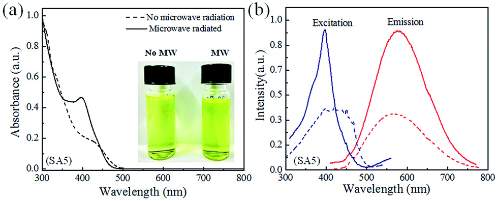 | ||
| Fig. 1 (a) Normalized UV-vis absorption spectrum of 2% Mn2+doped CdSe QDs (SA5) with microwave radiation (solid line) and without microwave (MW) radiation (dashed line). Inset shows the photographs of CdSe QDs solution before and after MW treatment. (b) Photoluminescence excitation and emission spectrum of the same SA5 sample with microwave radiation (solid line) and without microwave radiation (dashed line) respectively. | ||
Normalized photoluminescence (PL) excitation and emission spectra of the same 2% Mn2+ doped CdSe QDs (SA5) solution are shown in Fig. 1b before and after microwave irradiation keeping the emission wavelength fixed at 580 nm and excitation wavelength fixed at 377 nm respectively. From this result, it is observed that the excitation peak of the sample after microwave irradiation is enhanced in terms of sharpness and intensity which is found to be consistent with the UV-vis results of the same sample. The peak position of PL excitation spectra is also blue shifted to 397 nm after the microwave irradiation which indicates increase in band gap of the sample as observed in Fig. 1b. Considerably sharper absorption edge appeared in the PL excitation spectra after microwave irradiation due to the modified surface property of QDs and narrower size distribution as found in UV-vis spectra also. The PL emission peak at 574 nm is observed to be almost same for both the samples instead of intensity enhancement after microwave irradiation. Broad emission peak in terms of full width at half maximum (FWHM) is observed for the sample without microwave irradiation as non-radiative decay was high due to presence of higher number of surface defect states. Whereas sharp and narrow emission peak is observed in microwave irradiated sample which justifies the role of microwave radiation in producing almost homogeneous nanocrystal structures with less defects states on QDs surface. The normalized PL emission spectra of sample SA5 for different pH values from 9.5 to 11 after microwave treatment were also recorded as shown in Fig. S3b in the ESI† to show the effect of pH value on emission property of CdSe QDs. It has been observed that the emission peaks are red-shifting from 574 nm to 623 nm with the increase of pH value of the growth solution. This reveals that the non-radiative relaxation of the sample with pH value 9.5 was less compared to other samples as stokes shift is minimum for that QDs sample as shown in Fig. S3b in the ESI.†
Normalized electronic UV-vis absorption and PL spectra (excitation and emission) were recorded for all five sample as described in Table 1 with varying Mn2+ dopant concentration from 0 to 2 wt% relative to Cd2+ precursor as shown in Fig. 2a and b respectively. The absorption peak position for all the samples were appearing at ∼397 nm. However, this indicates that the band edge absorption of the incident photons for all the samples remains unaltered after dopant impurity incorporation in the host CdSe QDs. The nanoparticle radius R was estimated using the quantum confinement equation written in the form:20
 | (1) |
| CdSe sample name (for 80 mL solvent) | Cadmium acetate (mmol) | Manganese acetate (μmol) | 3-MPA (mmol) | Sodium selenosulfate (mmol) |
|---|---|---|---|---|
| SA1: undoped | 0.5 (133.26 mg) | 0.0 | 1.15 (122 mg) | 0.25 (19.74 mg) |
| SA2: 0.1 wt% Mn2+ | 0.5 (133.26 mg) | 0.5 (0.12 mg) | 1.15 (122 mg) | 0.25 (19.74 mg) |
| SA3: 0.2 wt% Mn2+ | 0.5 (133.26 mg) | 1.0 (0.25 mg) | 1.15 (122 mg) | 0.25 (19.74 mg) |
| SA4: 1.0 wt% Mn2+ | 0.5 (133.26 mg) | 5.0 (1.23 mg) | 1.15 (122 mg) | 0.25 (19.74 mg) |
| SA5: 2.0 wt% Mn2+ | 0.5 (133.26 mg) | 10.0 (2.45 mg) | 1.15 (122 mg) | 0.25 (19.74 mg) |
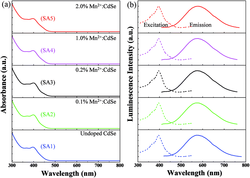 | ||
| Fig. 2 (a) Normalized UV-vis absorption and (b) PL excitation (dashed line) and emission (solid line) spectra of all five CdSe QDs sample with various Mn2+-dopant ion concentration synthesized in aqueous medium. | ||
2.2 Structural and compositional characterizations
The growth of CdSe QDs for all samples have been further characterized by powder XRD measurements and transmission electron microscopy (TEM) including HR-TEM, SAED, and FFT of HR-TEM image. The doping of Mn2+ as impurity atoms in the CdSe host material might influence to alter the lattice parameter slightly because the radius of the Mn2+ ion (70 pm) is smaller than that of the Cd2+ ion (95 pm).23 This change might not be observed as dopant concentrations were very low. To confirm the invariant crystal structure of all doped CdSe samples with the undoped CdSe QDs host, the powder XRD pattern of all five samples were recorded between 2θ values 20° to 80° as shown in Fig. 3a. The XRD pattern for all the samples shows the characteristic peaks at 2θ values about 25.4°, 42.5°, and 49.9° corresponding to the (111), (220), and (311) lattice planes of zinc blende phase of CdSe QDs supported by JCPDS PDF no. 19-0191. Therefore, it confirms that the crystal structure of the CdSe host material is unaltered after incorporation of dopant Mn2+ ions. It has also been observed that the peaks are broadened for all the five QDs samples. The factors related to this XRD peak broadening are crystallite domain size reduction, the strain produced by crystal lattice distortion due to dislocations and concentration gradients in non-stoichiometric crystals. Calculation shows that the crystalline domain size (D) was about 2.10 ± 0.69 nm from the observed line broadening in the XRD-spectrum by considering the instrumental line broadening. This value was estimated from the half bandwidth (FWHM) of the corresponding XRD peak by the Scherrer formula as given below.
 | (2) |
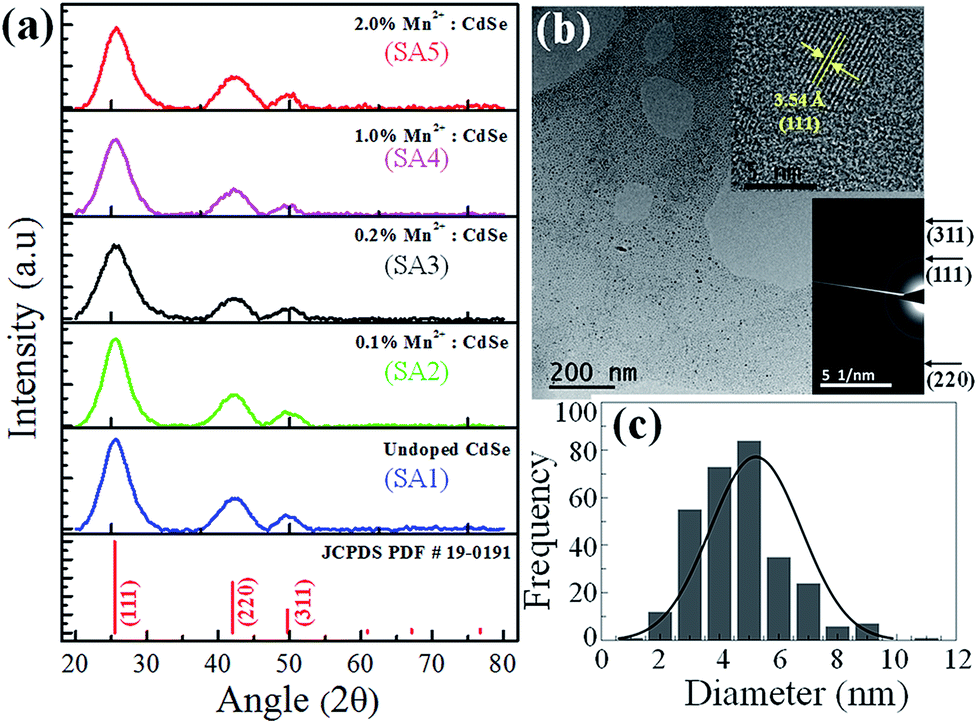 | ||
| Fig. 3 (a) Powder XRD spectrum of CdSe QDs with different Mn2+ concentrations along with standard JCPDS file number 19-0191 lines for bulk CdSe. (b) TEM image of 2% Mn2+ doped CdSe QDs (SA5). Inset (top right) shows the HR-TEM image of a CdSe nanoparticle with well-defined lattice planes of d spacing 3.54 Å. Inset (bottom right) shows SAED pattern of the same sample for crystal planes (111), (220), and (311). (c) Histogram profile of CdSe QDs size derived from (b). | ||
Transmission electron microscopy (TEM) was performed to visualize the actual size and crystal structure of the undoped and doped CdSe QDs samples. Fig. 3b shows the low-resolution TEM image of the 2% Mn2+ doped CdSe QDs sample (SA5). It shows isolated particles over the fields of view which is ruling out of QDs agglomeration. Size distribution of QDs sample is estimated with the maximum located at 5.2 nm from the histogram data extracted from the low-resolution TEM image shown in Fig. 3c. Top right inset of Fig. 3b is the HR-TEM image of one QD of the sample SA5 with calculated d-spacing 3.54 Å from the lattice planes in it. This is very close to the lattice spacing (d) value of the plane (111) for zinc blende crystal phase of CdSe nanoparticles verified by the JCPDS PDF no. 19-0191. This HR-TEM image also shows the QDs diameter of 5.5 nm which is very close to the mean diameter estimated from histogram profile (Fig. 3c) and UV-vis data of QDs solution. SAED pattern of the same 2% doped sample SA5 was recorded to see the diffraction pattern in reciprocal space and estimated the d-values from that as shown in the lower right inset of Fig. 3b. It is showing the bright circular ring for crystal planes (111), (220), and (311) corresponding to d-values 3.48 Å, 2.14 Å, and 1.78 Å respectively. This result is supporting again the earlier findings related to the size and crystal structure of all CdSe QDs samples synthesized in the aqueous medium at room temperature.
The chemical composition of the CdSe QDs samples was characterized with XPS, EDS, and ICP-AES measurements. XPS survey scan spectrum of 2% Mn2+-doped CdSe QDs sample (SA5) showed strong Cd and Se peaks as substantial evidence of CdSe QDs composition as shown in Fig. 4a. S peak is appeared in this because of the presence of thiol group with the 3-MPA ligand molecules. High-resolution spectrum of Cd 3d was recorded, and it is showing two peaks with binding energy (BE) at 405.9 and 412.8 eV, representing Cd 3d5/2 and Cd 3d3/2 states of Cd(II) respectively as shown in Fig. 4b. Similarly, the high-resolution spectrum of Se 3d is showing binding energy peak at 55.8 eV without any energy splitting as shown in Fig. 4c. Survey scan, Cd 3d, and Se 3d spectra for undoped CdSe QDs sample (SA1) are also showing almost similar results like SA5 as shown in ESI Fig. S5a, S5b and S5c† respectively. Multiplet splitting of the photoelectron peak from an individual core level will appear in the fine structure spectrum for a compound that has unpaired electrons in the valence band.25 It originates from the all possible spin distribution of the electrons in the energy band structure. This multiplet splitting effect has been already observed for the Mn 2p level in different compounds as doublet states like Mn 2p3/2 and Mn 2p1/2.26,27 These two states of the dopant atom Mn(II) appeared at binding energy 641.7 and 652.6 eV respectively in the high-resolution spectrum of sample SA5 as shown in Fig. 4d. This XPS study thus confirms the incorporation of Mn2+ as the dopant in CdSe QDs during growth in the aqueous medium. Undoped CdSe QDs sample SA1 is not showing any peak for Mn(II) as shown in ESI Fig. S5d.† The stoichiometric composition of the QDs particles was further obtained from EDS characterizations. The peaks confirm the presence of Cd, Se, and Mn for doped samples SA5 as shown in ESI Fig. S6.† The peak at 2.3 eV corresponds to sulfur (S) which is coming from the thiol group present in 3-MPA ligand molecules. The ratio of the peaks is in good agreement with the expected elemental compositions as shown in ESI Table S1† in terms of atomic% for all samples. Presence of Mn(II) in doped CdSe samples was further supported by recording inductively coupled plasma atomic emission spectroscopy (ICP-AES) as depicted in ESI Table S2.† From this Table S2,† it is evident that the Mn2+ incorporation as the dopant in CdSe QDs was successful via aqueous synthesis method.
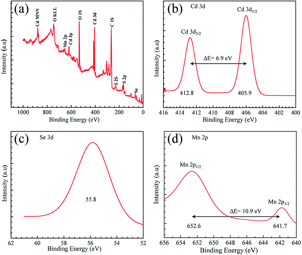 | ||
| Fig. 4 (a) Survey X-ray photoelectron spectrum of 2% Mn2+-doped CdSe QDs (SA5). (b) & (c) High-resolution spectrum of Cd 3d electrons showing doublet splitting with binding energy separated by 6.9 eV and Se 3d respectively. (d) High-resolution spectrum of Mn 2p core electrons showing doublet splitting with binding energy separated by 10.9 eV. | ||
2.3 Thin film devices fabrication via LBL electrostatic assembly method
Thin films of CdSe QDs (undoped and doped) were deposited with the help of layer-by-layer (LBL) electrostatic self-assembly (ESA) method using 5 mM PAH solution as the polycationic counterpart. A dipping sequence of PAH/CdSe resulted in LBL films of the quantum dots (QDs). Before starting of thin film deposition, QDs solution was purified with the help of non-solvent precipitation method as described in Experimental section. Electronic absorption spectra of the (PAH/CdSe)n LBL thin films were recorded after every (PAH/CdSe) layer deposition as shown in Fig. 5a. Here, the suffix ‘n’ represents the number of dipping cycles. It has been observed that, while depositing the LBL films with the polycation (PAH), band intensities of electronic absorption spectra of the QDs are increasing with the number of (PAH/CdSe) layers (Fig. 5a). The graph between the absorbance at the peak intensities (here 400 nm) of the QDs thin films versus the number of (PAH/CdSe) layers is showing linear through the origin which indicates uniform deposition of the QDs layers during the LBL film growth as shown in the inset of Fig. 5a.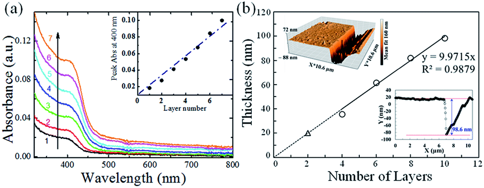 | ||
| Fig. 5 (a) The electronic absorption spectra of undoped CdSe QDs after every (PAH/CdSe) bilayer deposition using layer-by-layer (LBL) electrostatic assembly method on quartz substrate. The inset shows peak absorbance as a function of the number of layers. (b) Plot of the thickness of (PAH/CdSe)n films deposited via LBL electrostatic assembly method versus number of layers (n). The line, which has been extrapolated to estimate the thickness of monolayer, is the best fit to the points. Insets shows 3-dimensional AFM topographic image (top) of a scratch on (PAH/CdSe)10 film and the obtained depth (bottom) in the line profile of the scratch. | ||
It has been observed that the peak absorption of CdSe QDs was redshifted to 400 nm in the thin film compared to that measured at 397 nm in dispersed solution. This 400 nm absorption peak corresponds to the QDs size of 5.4 nm, which is not the integral multiple of actual QDs size 5.3 nm calculated from the optical Tauc plot. Therefore, this red-shift in the absorbance spectrum cannot be originated by the formation of clusters in the film. The shift could be due to the electrostatic interaction between carboxyl (–COO−) functional group and amine (–NH3+) groups on the surfaces of CdSe and the polycation, respectively, in thin films. The close packed geometry of QDs in the LBL film might also result in the energy band shift towards red. The presence of carboxyl functional group –COO− on the surface of CdSe QDs samples was confirmed by recording the FT-IR spectra of CdSe QDs and 3-MPA as presented in ESI Fig. S7† with a short note. It shows the presence of most of the vibration bands in QDs spectrum as in 3-MPA spectrum. Since LBL film deposition depends on the electrostatic attraction with surface charge reversal during growth of every (PAH/CdSe) layer, deposition of a monolayer is assured with a formation of a two-dimensional array of QDs on a selected substrate.
Topographic images of mechanically scratched films were recorded using atomic force microscope (AFM) to support the above finding as shown in Fig. 5b. Since one or two bilayer films are anticipated to have too low thickness, we performed these topographic measurements on films of 4 or more bilayer numbers. The thickness of scratched films versus layer numbers of (PAH/CdSe) is shown in Fig. 5b. Three-dimensional (3D) view of an AFM topography image and the depth on the line profile of the scratched film for 10 layers are also shown in the insets of Fig. 5b. The Fig. 5b shows that the thickness of the film increases uniformly with the number of deposited QDs layers. The linear fit of the plot shows that it approaches the origin. From the extrapolated part of the fitted line, the thickness of a monolayer (PAH/CdSe) film was estimated. It has reflected a value of ∼10 nm, which can be considered as the sum of the thicknesses of a PAH layer and the diameter of CdSe QDs. The value is quite fair considering the diameter of CdSe nanoparticles (∼5.3 nm) obtained from other characterizations technique.
2.4 Current–voltage (I–V) characteristics of LBL thin films
Since the CdSe quantum dots (QDs) samples were doped with Mn2+ as impurity atoms with varying concentration, it is intriguing to measure current–voltage (I–V) characteristics of the LBL thin film devices for all samples and compare the results among them to determine the effect of doping on electrical conductivity. Current–voltage (I–V) characteristics of all the fabricated devices [ITO/(PAH/CdSe)10/Al] using undoped and four Mn2+-doped CdSe QDs samples are measured by sweeping the voltage between +1 V to 1 V as shown in Fig. 6a. The device of undoped CdSe QDs (SA1) such as ITO/(PAH/CdSe)10/Al has shown the highest resistivity between this applied voltage range as shown in Fig. 6a using the blue coloured continuous line. It has been observed from the current–voltage (I–V) characteristics that the conductivity of the CdSe QDs devices are augmenting with the increase of Mn2+ dopant ion concentration in the CdSe QDs host. Conductivity is enhanced by the order of 104 between undoped (SA1) and 2% Mn2+-doped CdSe QDs (SA5) sample based devices as shown in Fig. 6a. Impurity doping introduces this colossal conductivity enhancement in CdSe QDs synthesized in the aqueous medium under ambient condition keeping the size of QDs samples constant as established earlier using UV-vis and TEM study. As the size of all QDs samples were similar, their bandgaps are also almost equal. So the bandgap has no role on this conductivity enhancement among all QDs samples. Therefore, the conductivity of the thin film devices are solely dependent on the concentration of Mn2+ dopant ions in the CdSe QDs samples. Interestingly, Mn2+ dopant ions in CdSe are the source of charge carriers due to the ‘auto-ionization’ without thermal activation as the size of CdSe samples were well below the critical diameter for this effect.12 When the diameter of doped QDs reaches a small critical value, the Coulomb attraction energy between the valence electron and its atomic core will become weaker than the confined electronic states of nanoparticle host. As a result, these carriers occupy an energy state of the quantum dot automatically.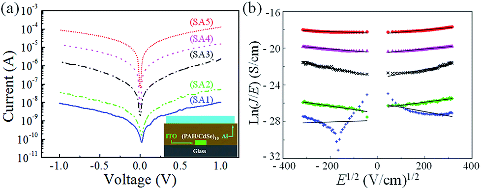 | ||
| Fig. 6 (a) Current–voltage (I–V) characteristics of all the five devices similar to ITO/(PAH/X)10/Al. Here X is different CdSe QDs sample with varying doping concentration like undoped (SA1, solid blue line), 0.1% doped (SA2, green dash dot line), 0.2% doped (SA3, black dash dot line), 1.0% doped (SA4, pink dash line), and 2.0% doped (SA5, red dotted line). Inset shows the schematics of the cross-sectional view of the devices. (b) Poole–Frenkel fitting for all samples with respective straight trend line. The lines are best fits to the experimental points in each of the cases except undoped sample. | ||
In Fig. 6b the field dependent conductivity plots are shown as the Poole–Frenkel representation ln(J/E) versus E1/2 for all five samples at ambient temperature. The Fig. 6b clearly shows that in the chosen model the ln(J/E) versus E1/2 curves are showing very nice straight line fitting as described in the Poole–Frenkel effect with the equation below.28
 | (3) |
2.5 STM study of monolayer QDs films
Memristor characterizations were performed in ambient conditions using scanning tunneling microscope (STM) tip as another electrode in constant current mode following measurement schematics as shown in inset of Fig. 7a. High conducting As doped n-type Si(111) substrate is used as bottom electrode on which 2D array of CdSe QDs samples were deposited in the form of monolayer thin films. 2D array of CdSe QDs samples were deposited over the Si substrate using LBL electrostatic attraction between cationic amine (–NH3+) functional groups of PAH and anionic carboxyl (–COO−) functional group on QDs surface. And this is evidenced by several techniques like UV-vis absorption spectra and AFM topographic images of scratched thin films. The Pt/Ir tip was approached with a set point of tunneling current of 1 nA at tip bias voltage of 1.5 V with respect to Si(111) substrate. All parameters including PID values of imaging mode were kept same throughout all STM measurements. The topographic image of bare silicon without CdSe quantum dots layer is recorded using the same set point to show the smoothness of substrate as shown in inset of Fig. 7c. It was showing RMS area roughness < 1.6 Å. Monolayer growth and distribution of QDs on Si(111) wafer was confirmed again from STM topographic image as shown in inset of Fig. 7d. The RMS area roughness has increased to ∼25.4 Å with the deposited CdSe QDs monolayer as described in Experimental section. This topographic image also depicts the morphology of the CdSe QDs array on Si(111) with clear visualization about the presence of QDs. To measure the tunneling current of CdSe QDs samples as 2D array, the STM tip voltage was scanned from −3 V to +3 V between the Si(111) substrate and STM tip under both voltage sweep directions (forward and backward) as shown in Fig. 7a and b for undoped CdSe (SA1) and 0.2% Mn2+-doped CdSe QDs (SA3) sample respectively. The 0.2% doped CdSe QDs (SA3) is switched to a high conducting state at a positive bias, here it is +2.5 V as shown in Fig. 7b. It is called as the threshold voltage (VTh) of resistive switching. The QDs monolayer devices were switched back to their original low conducting state when the tip voltage sweeps towards 3.0 V as shown in Fig. 7b. The ON/OFF ratio observed for the monolayer device of 0.2% Mn2+-doped CdSe QDs sample (SA3) is higher than 102 as plotted in inset of Fig. 7b. Such a resistive switching is reproducible over many cycles. The tunneling current measurements were performed for all other samples including bare Si(111) following the same measurement procedure and results are shown in ESI Fig. S8.† The results depict that a single CdSe QD or a parallel combination of it (two-dimensional array) exhibits electrical bistability compared to undoped CdSe QDs sample for this 3 V bias range. It has been observed by comparing the threshold voltage of switching (VTh) among all CdSe QDs samples that the VTh is decreasing with the higher doping concentration. Variation of the maximum sweep voltage (VMax) yields the similar VTh and almost identical resistive switching property as shown in the ESI Fig. S9.† Measurements at different locations on the same QDs film have also shown almost similar behaviour (Fig. S10 in the ESI†).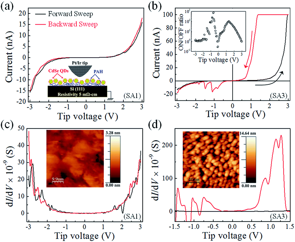 | ||
| Fig. 7 (a) and (b) Tunneling current–voltage (I–V) characteristics of a monolayer of undoped (SA1) and 0.2% Mn2+-doped CdSe QDs (SA3) with the Pt/Ir tip of scanning tunneling microscope respectively. Undoped CdSe is showing the almost identical current for the voltage-sweep in the forward- and backward directions. Doped CdSe is showing low conducting state (OFF state, black line) and high conducting state (ON state, red line) for forward and backward voltage sweep direction respectively. Inset of (a) shows the monolayer device schematics for STM measurements. Inset of (b) shows ON/OFF ratio vs. tip voltage curve calculated from the I–V data plotted in (b). (c) and (d) Differential conductance–voltage characteristics of a monolayer of undoped (SA1) and 0.2% Mn2+-doped CdSe QDs (SA3) respectively in their forward (black line) and backward (red line) sweep direction. Inset of (c) shows the topographic image of bare Si(111). Inset of (d) shows the topographic image of a monolayer of undoped CdSe QDs deposited on Si(111) representing the presence of QDs on the substrate. All STM topographic images are processed using WSxM software. | ||
It is promising in terms of the future technological impact that resistive switching appears in the two-dimensional array of doped CdSe QDs samples in the voltage range of ±3 V which is absent for undoped CdSe QDs film as shown in Fig. 7a. It indicates that a state (high or low) can be stored in a single Mn2+ doped CdSe QDs for low-power high-density memory applications. As the monolayers of undoped CdSe QDs did not yield any resistive switching in that voltage range, they needed a much higher voltage amplitude to evidence conductance switching.30 The results hence explore the advantages of Mn2+ dopant ions incorporation as the impurity in CdSe QDs host for memristor application with lower threshold switching voltage (VTh). Therefore, this robust QDs synthesis method in the aqueous medium under ambient condition allows varying the doping concentration efficiently with high yield. These results explore the future demand of a suitably doped CdSe QDs sample which is capable to switch at a particular VTh. Highly doped n-type Si(111) substrate and Pt/Ir tip with the work function of 4.9 eV and 5.6 eV respectively served as the electrodes in STM measurements. Here, resistive switching to a high conducting state appeared at a positive tip voltage. Since the tip voltage was always applied to the Si(111) substrate, the results hence demonstrate that the conductance switching occurs when a positive voltage higher than VTh is applied to the high work function electrode. The barrier height faced by the charge carriers has a major role in the observed conductance switching.
A debate is always there about the exact mechanism of resistive switching. Therefore, it is a real challenge to identify the exact mechanism of resistive switching of these CdSe QDs thin films. Calculation of density of states (DOS) before and after resistive switching must be a strong evidence to highlight the mechanism indirectly. Fig. 7c and d shows the plots of dI/dV versus voltage (V) for both the sweep directions, as obtained from the I–V characteristics of a monolayer of SA1 and SA3 sample respectively with Pt/Ir STM tip as the top electrode. The Fig. 7d shows that the calculated total DOS for the high conducting state is increased a lot compared to the low conducting state. Here, the total DOS can be calculated from the area under the dI/dV versus voltage curves. For the monolayer of undoped CdSe QDs, there was no noticeable change in the density of states (DOS) for both the voltage sweep direction as shown in Fig. 7c. This enhancement of DOS for the low resistive state supports both the charge confinement in doped CdSe QDs and the presence of free carriers due to the auto-ionization of dopant atoms in doped CdSe QDs as compared to the undoped one.
3. Conclusion
In conclusion, we have demonstrated a cost-effective method to tune the electrical conductivity of CdSe QDs thin films by varying the doping concentration. High-quality 3-MPA capped Mn2+-doped CdSe QDs samples were synthesized in the aqueous medium under ambient condition. Experimental results show the variation of Mn2+ dopant is possible by keeping the size of CdSe QDs samples invariant. In this way, we have decoupled the optical and electronic properties of CdSe QDs to study the effect of doping only on its electrical conductivity. The advantage of the use of short-chain capping ligand 3-MPA is to minimize the barrier energy for the charge carriers transport in QDs thin films. Microwave heating of QDs growth solution shows a remarkable improvement of optical properties and size distribution. Structural characterizations show zinc-blende crystal phase of all QDs samples which was desirable to overcome the hurdle of Mn2+-doping in CdSe QDs. Results from composition study also indicate high doping yield in as-synthesized CdSe QDs in the aqueous medium. Poole–Frenkel fitting of the I–V results shows that the mechanism of carrier transport is due to the electric field assisted thermal ionization of dopants to generate charge carriers in CdSe QDs. This result can be interpretable with the help of ‘auto-ionization’ effect of dopants in CdSe QDs as its sizes are less than the critical diameter. This analysis shows substantial evidence for the presence of the dopant in CdSe QDs either in the core or on the surface. Finally, STM I–V results depict the resistive switching property of monolayer CdSe QDs films. Our results demonstrate that the threshold voltage (VTh) of resistive switching was also decreasing with the increase of Mn2+ dopant concentration in CdSe QDs which is a step forward to minimize the energy consumption per byte of the resistive data storage devices in future.4. Experimental section
4.1 Chemicals & materials
Cadmium acetate dihydrate [Cd(CH3COO)2·2H2O, 98%], manganese acetate tetrahydrate [Mn(CH3COO)2·4H2O, 99.99%], selenium powder (Se, 99.99%), sodium sulfite anhydrous (Na2SO3, ≥98%, Aldrich), and 3-mercaptopropionic acid (3-MPA, ≥99%) were purchased from Sigma Aldrich as source of precursors to grow the quantum dots and surface capping ligands to stabilize these quantum dots in aqueous solution. NaOH beads and ammonium hydroxide solution (NH4OH, 25%) were purchased from Merck to adjust pH of the Cd-precursor solutions during growth of quantum dots in water. All the chemicals were used as received without further purification. Deionized water of resistivity of 18.2 MΩ cm obtained from Milli-Q Direct 8 system is used for the entire research work. Poly(allylamine hydrochloride) (PAH, MW = 120 k to 200 k) was purchased from Alfa Aesar and used as inert cationic polymer to deposit layer-by-layer (LBL) thin films of negatively charged 3-MPA capped CdSe QDs with the help of electrostatic self-assembly (ESA) technique. ITO-coated glass substrates of sheet resistance 10−15 ohm cm−2 for crossbar sandwich type thin film devices fabrication were purchased from Optical Filters Inc., UK. Polished high conducting arsenic-doped n-type Si(111) wafers with resistivity < 5 mΩ cm were used as the substrates to deposit 2D array of CdSe QDs as monolayer devices for STM study and purchased from Silicon Valley Microelectronics (SVM) Incorporation, USA. Acetone [(CH3)2CO] and isopropanol [(CH3)2CHOH] were used for cleaning purpose. Hydrochloric acid (HCl), hydrofluoric acid (HF), and hydrogen peroxide (H2O2, 30% w/v) were used as purchased for substrates cleaning and the removal of native. SiO2 layer from high conducting As doped Si(111) substrate following standard protocol.4.2 Synthesis of CdSe quantum dots (QDs)
To synthesize undoped CdSe QDs in aqueous medium, we have used cadmium acetate as Cd2+ precursor, sodium selenosulfate (Na2SeSO3) as Se2− precursor, and 3-MPA as stabilizing ligand with modified literature approach.30,31 Briefly, cadmium acetate (133.26 mg, 0.5 mmol) was dissolved in 80 mL Milli-Q water with continuous vigorous stirring at room temperature (∼24 °C). Then 3-MPA (122 mg, 1.15 mmol) was added to the above solution with continuous stirring and instantly the color of the solution becomes white turbid. Then the solution was made alkaline at pH value 9.5 by adding NH4OH solution dropwise (pH value would be above 12 by using NaOH solution) and the precursor solution became colorless. After that, freshly prepared sodium selenosulfate (19.74 mg, 0.25 mmol) as Se2− precursor was injected to the above solution under continuous stirring. Here Na2SeSO3 is prepared by refluxing 2 g of selenium and 4.83 g of sodium sulfite in 100 mL of water for 10 h. After few minutes, the solution became light greenish yellow in color. This was the indication to start nucleation of CdSe QDs and this solution was continuously stirred for another 2 hours to give enough time for further QDs growth. Then the resultant CdSe QDs solution was placed under microwave irradiation as the final step of this QDs growth under ambient condition in aqueous medium. The condition of microwave irradiation was maintained in three consecutive steps of time duration 60 seconds with power set at 450 W (operational frequency 2.45 GHz) using Samsung 20L oven (Model no. MW73AD-B/XLT). After that the colour of the QDs solution become bright greenish yellow as the indication of completed growth of quantum dots (QDs) in water. The mole ratio of precursors and ligand molecules for the synthesis of undoped CdSe QDs (SA1) is shown in Table 1.324.3 Synthesis of Mn2+-doped CdSe QDs
Four more CdSe QDs samples were synthesized by varying Mn2+ concentration as impurity atom or dopant. Doped samples SA2, SA3, SA4, & SA5 were synthesized following the same protocol like sample SA1 by adding an adequate amount of manganese acetate as dopant precursor into the cadmium precursor solution from the beginning. The doping concentration was estimated for different samples by calculating the mole ratio between Cd2+ and Mn2+ precursors as shown in Table 1. Optical properties of all the samples (undoped & doped) were always kept invariant by selecting CdSe QDs growth in solution of constant volume. All QDs sample were further purified with the help of non-solvent based precipitation technique.32 Here we had added acetonitrile slightly higher than the volume of QDs sample and after some time yellow colour precipitation (ppt) was formed. After removal of supernatant, yellow coloured precipitate (ppt) was re-dispersed again in Milli-Q water. We have repeated this method two more time to purify CdSe samples as much as possible. Then, we did centrifugation at a speed of 3000 rpm and 4 °C temperature to form ppt. Finally, we removed the supernatant completely and dried out in vacuum. These purified QDs samples have been used for further characterizations and devices fabrication by mixing with DI water of same volume at the beginning of purification step.4.4 Characterization of QDs
Several characterizations were performed to confirm the growth of CdSe QDs and successful incorporation of Mn2+ atoms as dopant in CdSe QDs. Electronic UV-vis absorption spectra of the QDs samples dispersed in water were recorded with a PerkinElmer LAMBDA 950 UV/Vis/NIR Spectrophotometer. Photoluminescence (PL) spectroscopy of the QDs samples were performed with a Horiba NanoLog Spectrofluorometer. Presence of capping agent or the ligand molecules as stabilizer on the surface of QDs was verified using Shimadzu IRPrestige Fourier Transform Infrared (FTIR) Spectrometer. The crystallinity of undoped and doped CdSe QDs samples were analyzed with powder X-ray diffraction (XRD) spectrum obtained from PANalytical Empyrean Spectrometer. The sample was made into fine powder to get XRD spectrum and the intensity of diffracted signal was recorded in terms of 2θ from 20° to 80°. Size and crystal phase of QDs were further characterized using the TEM, high resolution TEM (HR-TEM), selected area electron diffraction (SAED), and fast Fourier transform (FFT) data from 300 kV FE5I TECHNAI G2-TF-30 Transmission Electron Microscope (TEM). Composition of QDs was characterized using energy-dispersive X-ray spectroscopy (EDS), inductively coupled plasma atomic emission spectroscopy (ICP-AES), and X-ray photoelectron spectroscopy (XPS) data. The element-wise composition of the QDs was determined by collecting EDS data using Apollo X EDS system coupled with a Nova Nano SEM 450 field-emission scanning electron microscope (SEM). ICP-AES data of our samples were recorded using ARCOS, Simultaneous ICP Spectrometer. XPS data of QDs samples were recorded using Omicron ESCA 2SR XPS system. The binding energies were adjusted for the energy shift using the C 1s peak of graphitic carbon (BE = 285.4 eV) as a reference.4.5 Thin film devices fabrication
QDs thin film device were fabricated using the following architectures like ITO/(PAH/QDs)10/Al as multilayer device and Si(111)/(PAH/QDs)01/STM tip as a monolayer device. The 3-MPA capped QDs layers were deposited using layer-by-layer (LBL) electrostatic self-assembly (ESA) method on substrates like ITO and silicon to fabricate multilayer or monolayer thin film devices using PAH as cationic counterpart following standard reported protocol. Briefly, substrates were sonicated in soap solution, DI water, acetone![[thin space (1/6-em)]](https://www.rsc.org/images/entities/char_2009.gif) :IPA (1:1) for 15 minutes and 3 times each to clean, then dried and kept in vacuum. Before depositing QDs layer, substrates were deprotonated by keeping in a mixture of NH4OH and H2O2 with ratio (3:1 v/v) for more than 2 hours. These substrate were then rinsed in DI water thoroughly after removal and dried before further use. Additional treatments for Si(111) substrate was performed when required to remove native oxide layer. To remove particulate contaminants, Si substrates were dipped in a mixture of NH4OH (25%), H2O2 (30%) and H2O in the ratio of 1:2:10 and heated at 70 °C for 10 minutes. Then, a solution of HCl (32%):H2O2 (30%):H2O in the proportion of 1:1:5 used to heat at 70 °C for 10 minutes to dissolve alkali ions and hydroxides from the surface of Si substrates. Then it was dipped in dilute 2% hydrofluoric acid (HF) in water for 2 minutes to remove the native SiO2 layer. UV–ozone cleaning was performed as the final step before starting of LBL devices fabrication to make Si(111) surface hydrophilic. To deposit monolayer of QDs, cleaned Si substrates were dipped in the cationic PAH bath for 15 min followed by rinsing in water bath for three times (2:2:1 minute). Here the concentration used to make PAH bath was 5 mM and the pH value of this adjusted to 6.5 using dilute NaOH for this entire work. Then the PAH-coated substrates were dipped in the 3-MPA capped negatively charged CdSe QDs solution for 15 min followed by the same rinsing process in water bath to obtain a 2 dimensional array of QDs as monolayer on Si(111) substrate.33 These monolayer film of QDs [Si(111)/(PAH/QDs)] were used for further STM study to record I–V characteristics. To fabricate multi-layer thin film devices, the QDs deposition process for monolayer thin film was repeated for the desired layer numbers, say, for 10 layers device it was ITO/(PAH/QDs)10. The electronic UV-vis absorption spectrum is also recorded by repeating the (PAH/QDs) layer deposition sequence in cycles on quartz substrates to monitor the thin film growth. To monitor layer growth further, AFM topography of scratched films were recorded in “Dynamic force” mode to measure the thickness directly using Naio AFM supplied by Nanosurf, Switzerland at tip set point 50%. After growing 10 bilayer CdSe QDs samples on ITO, the films were annealed in vacuum at 110 °C for overnight to remove residual solvents. At last, aluminum (Al) top electrodes were deposited with the help of pre-designed metal shadow mask to complete devices fabrication process using Kurt J. Lesker PVD75 thermal evaporator system at pressure ∼ 10−6 torr. Thickness of the Al electrode was maintained about 80 nm for all devices as indicated by quartz crystal thickness monitor. Top Al electrodes were aligned as perpendicular compared to the bottom ITO electrode to form cross-bar junction. These multi-layer thick devices were used for further electrical characterizations using Keithley 4200 SCS parameter analyzer by making electrical contacts inside Janis ST-500 probe station under vacuum at ∼10−5 torr at room temperature (∼24 °C).
:IPA (1:1) for 15 minutes and 3 times each to clean, then dried and kept in vacuum. Before depositing QDs layer, substrates were deprotonated by keeping in a mixture of NH4OH and H2O2 with ratio (3:1 v/v) for more than 2 hours. These substrate were then rinsed in DI water thoroughly after removal and dried before further use. Additional treatments for Si(111) substrate was performed when required to remove native oxide layer. To remove particulate contaminants, Si substrates were dipped in a mixture of NH4OH (25%), H2O2 (30%) and H2O in the ratio of 1:2:10 and heated at 70 °C for 10 minutes. Then, a solution of HCl (32%):H2O2 (30%):H2O in the proportion of 1:1:5 used to heat at 70 °C for 10 minutes to dissolve alkali ions and hydroxides from the surface of Si substrates. Then it was dipped in dilute 2% hydrofluoric acid (HF) in water for 2 minutes to remove the native SiO2 layer. UV–ozone cleaning was performed as the final step before starting of LBL devices fabrication to make Si(111) surface hydrophilic. To deposit monolayer of QDs, cleaned Si substrates were dipped in the cationic PAH bath for 15 min followed by rinsing in water bath for three times (2:2:1 minute). Here the concentration used to make PAH bath was 5 mM and the pH value of this adjusted to 6.5 using dilute NaOH for this entire work. Then the PAH-coated substrates were dipped in the 3-MPA capped negatively charged CdSe QDs solution for 15 min followed by the same rinsing process in water bath to obtain a 2 dimensional array of QDs as monolayer on Si(111) substrate.33 These monolayer film of QDs [Si(111)/(PAH/QDs)] were used for further STM study to record I–V characteristics. To fabricate multi-layer thin film devices, the QDs deposition process for monolayer thin film was repeated for the desired layer numbers, say, for 10 layers device it was ITO/(PAH/QDs)10. The electronic UV-vis absorption spectrum is also recorded by repeating the (PAH/QDs) layer deposition sequence in cycles on quartz substrates to monitor the thin film growth. To monitor layer growth further, AFM topography of scratched films were recorded in “Dynamic force” mode to measure the thickness directly using Naio AFM supplied by Nanosurf, Switzerland at tip set point 50%. After growing 10 bilayer CdSe QDs samples on ITO, the films were annealed in vacuum at 110 °C for overnight to remove residual solvents. At last, aluminum (Al) top electrodes were deposited with the help of pre-designed metal shadow mask to complete devices fabrication process using Kurt J. Lesker PVD75 thermal evaporator system at pressure ∼ 10−6 torr. Thickness of the Al electrode was maintained about 80 nm for all devices as indicated by quartz crystal thickness monitor. Top Al electrodes were aligned as perpendicular compared to the bottom ITO electrode to form cross-bar junction. These multi-layer thick devices were used for further electrical characterizations using Keithley 4200 SCS parameter analyzer by making electrical contacts inside Janis ST-500 probe station under vacuum at ∼10−5 torr at room temperature (∼24 °C).
4.6 Electrical characterizations
Current–voltage (I–V) characteristics of the QDs multi-layer thin film devices were measured at room temperature by sweeping voltage from 0 V to + 1.0 V to −1.0 V to 0 V in multiple cycles using step voltage 20 mV under vacuum of order ∼10−5 torr. The STM topography and I–V characteristics of the doped and undoped monolayer CdSe QDs were recorded using Scanning Tunneling Microscope (Nanosurf Naio STM) tip as another electrode. For this measurements, the Si(111) substrates were grounded using Ag paste with the metallic substrate holder. Mechanically cut very sharp Pt/Ir tips were used to sweep bias voltage and measure tunneling current. Every time the Pt/Ir tips were standardized for atomic sharpness by recording the topographic images of standard samples like gold and HOPG surface as shown in ESI Fig. S1a and S1b† respectively. If it produces very good topographic images available in literature then it is identified as good and atomically sharp tip for further use. The topographic images of HOPG and gold were recorded using the set current at 1 nA and tip bias voltage 50 mV. First, Pt/Ir tip was approached at a set point, tip voltage 1.5 V and set current 0.5 nA and then topographic images were recorded using “Imaging” mode. After achieving good topographic image of our samples, the inbuilt ‘Spectroscopy’ mode was used for further I–V measurements. Using the same tip, under the same approach conditions, tip bias voltage was swept in forward and backward direction between −VMax to +VMax and the corresponding tunneling current was measured between tip and sample. I–V measurements were recorded multiple times on several points on a particular QDS sample surface. All the STM experiments were performed under ambient conditions using constant current mode. STM topographic images are processed using WSxM software.34Conflicts of interest
There are no conflicts of interest to declare.Acknowledgements
This work is supported by the Indian Institute of Science Education and Research Thiruvananthapuram (IISER-TVM), the Ministry of Human Resource Development (MHRD), Government of India and the Science & Engineering Research Board (SERB), DST, Government of India through the projects EEQ/2016/000045 and ECR/2017/000630. BCD acknowledges the support from the UGC-UKIERI Joint Research Programme (UKIERI-III) with file no. 184-1/2018(IC). S. K. M., A. S., and S. S. acknowledges JRF fellowship for PhD work offered by IISER-TVM. S. A. acknowledges BS-MS studentship offered by IISER-TVM.References
- T. Chen, K. V. Reich, N. J. Kramer, H. Fu, U. R. Kortshagen and B. I. Shklovskii, Nat. Mater., 2015, 15, 299–303 CrossRef PubMed.
- D. V. Talapin, J.-S. Lee, M. V. Kovalenko and E. V. Shevchenko, Chem. Rev., 2010, 110, 389–458 CrossRef PubMed.
- A. Stavrinadis, A. K. Rath, F. P. G. de Arquer, S. L. Diedenhofen, C. Magen, L. Martinez, D. So and G. Konstantatos, Nat. Commun., 2013, 4, 2981 CrossRef PubMed.
- A. Nag and D. D. Sarma, J. Phys. Chem. C, 2007, 111, 13641–13644 CrossRef.
- H. Liu and P. Guyot-Sionnest, J. Phys. Chem. C, 2015, 119, 14797–14804 CrossRef.
- T. C. Harman, P. J. Taylor, M. P. Walsh and B. E. LaForge, Science, 2002, 297, 2229–2232 CrossRef PubMed.
- B. C. Das, S. K. Batabyal and A. J. Pal, Adv. Mater., 2007, 19, 4172–4176 CrossRef.
- A. Kongkanand, K. Tvrdy, K. Takechi, M. Kuno and P. V. Kamat, J. Am. Chem. Soc., 2008, 130, 4007–4015 CrossRef PubMed.
- B. C. Das and A. J. Pal, Small, 2008, 4, 542–547 CrossRef PubMed.
- C. R. Kagan and C. B. Murray, Nat. Nanotechnol., 2015, 10, 1013–1026 CrossRef PubMed.
- A. I. Ekimov, I. A. Kudryavtsev, M. G. Ivanov and A. L. Efros, J. Lumin., 1990, 46, 83–95 CrossRef.
- D. J. Norris, A. L. Efros and S. C. Erwin, Science, 2008, 319, 1776–1779 CrossRef PubMed.
- J. Yang, R. Fainblat, S. G. Kwon, F. Muckel, J. H. Yu, H. Terlinden, B. H. Kim, D. Iavarone, M. K. Choi, I. Y. Kim, I. Park, H.-K. Hong, J. Lee, J. S. Son, Z. Lee, K. Kang, S.-J. Hwang, G. Bacher and T. Hyeon, J. Am. Chem. Soc., 2015, 137, 12776–12779 CrossRef PubMed.
- A. Nag, R. Cherian, P. Mahadevan, A. V. Gopal, A. Hazarika, A. Mohan, A. S. Vengurlekar and D. D. Sarma, J. Phys. Chem. C, 2010, 114, 18323–18329 CrossRef.
- R. N. Bhargava, D. Gallagher, X. Hong and A. Nurmikko, Phys. Rev. Lett., 1994, 72, 416–419 CrossRef PubMed.
- S. Acharya, D. D. Sarma, N. R. Jana and N. Pradhan, J. Phys. Chem. Lett., 2010, 1, 485–488 CrossRef.
- S. C. Erwin, L. J. Zu, M. I. Haftel, A. L. Efros, T. A. Kennedy and D. J. Norris, Nature, 2005, 436, 91–94 CrossRef PubMed.
- L. G. Gutsev, N. S. Dalal and G. L. Gutsev, J. Phys. Chem. C, 2015, 119, 6261–6277 CrossRef.
- T. H. Chiang and J. F. Wager, IEEE Trans. Electron Devices, 2018, 65, 223–230 Search PubMed.
- U. E. H. Laheld and G. T. Einevoll, Phys. Rev. B: Condens. Matter Mater. Phys., 1997, 55, 5184–5204 CrossRef.
- T. A. Kennedy, E. R. Glaser, P. B. Klein and R. N. Bhargava, Phys. Rev. B: Condens. Matter Mater. Phys., 1995, 52, 14356–14359 CrossRef.
- R. Beaulac, P. I. Archer, J. van Rijssel, A. Meijerink and D. R. Gamelin, Nano Lett., 2008, 8, 2949–2953 CrossRef PubMed.
- C. H. Yoder, Ionic compounds: applications of chemistry to mineralogy, Wiley-Interscience, Hoboken, 2006 Search PubMed.
- V. Swamy, B. C. Muddle and Q. Dai, Appl. Phys. Lett., 2006, 89, 163118 CrossRef.
- C. R. Brundle, Electron spectroscopy: theory, techniques and applications, Academic Press, London, 1985 Search PubMed.
- G. W. Ewing and J. Cazes, Analytical instrumentation handbook, Marcel Dekker, Estados Unidos, 2005 Search PubMed.
- S. Ueda, A. Sekiyama, T. Iwasaki, S. Imada, S. Suga, Y. Saitoh, W. Giriat and S. Takeyama, Phys. Rev. B: Condens. Matter Mater. Phys., 2008, 78, 205206 CrossRef.
- D. Conklin, S. Nanayakkara, T.-H. Park, M. F. Lagadec, J. T. Stecher, M. J. Therien and D. A. Bonnell, Nano Lett., 2012, 12, 2414–2419 CrossRef PubMed.
- K. K. Ng and S. M. Sze, Physics of Semiconductor Devices, John Wiley & Sons Incorporated, 3rd edn, 2006 Search PubMed.
- B. Ghosh, B. C. Das and A. J. Pal, Small, 2010, 6, 52–57 CrossRef PubMed.
- H. Qian, X. Qiu, L. Li and J. Ren, J. Phys. Chem. B, 2006, 110, 9034–9040 CrossRef PubMed.
- A. L. Rogach, Semiconductor nanocrystal quantum dots: synthesis, assembly, spectroscopy, and applications, Springer, Wien, 2008 Search PubMed.
- G. Decher, Science, 1997, 277, 1232–1237 CrossRef.
- I. Horcas, R. Fernandez, J. M. Gomez-Rodriguez, J. Colchero, J. Gomez-Herrero and A. M. Baro, Rev. Sci. Instrum., 2007, 78, 013705 CrossRef PubMed.
Footnote |
| † Electronic supplementary information (ESI) available. See DOI: 10.1039/c8ra03631d |
| This journal is © The Royal Society of Chemistry 2018 |