
 Open Access Article
 This Open Access Article is licensed under a Creative Commons Attribution-Non Commercial 3.0 Unported Licence
A near-infrared photoinverter based on ZnO and quantum-dots
Byung Jun Kima,
Sungho Parka,
Soon Kyu Chab,
Il Ki Hanc and
Seong Jun Kang *a
*a
aDepartment of Advanced Materials Engineering for Information and Electronics, Kyung Hee University, Yongin 17104, Republic of Korea. E-mail: junkang@khu.ac.kr; Tel: +82-31-201-3324
bKHU-KIST Department of Converging Science and Technology, Kyung Hee University, Seoul 02447, Republic of Korea
cNanophotonics Research Center, Korea Institute of Science and Technology, Seoul 02792, Republic of Korea
First published on 27th June 2018
Abstract
Near-infrared (NIR) photoswitching transistors have been fabricated using a hybrid structure of zinc oxide (ZnO) and quantum-dots (QDs). The ZnO active layer was prepared using a solution process, while colloidal QDs were inserted between a silicon dioxide (SiO2) gate insulator and a ZnO active layer. The small band gap QDs (1.59 eV) were used to absorb low-energy NIR photons, generate photo-excited carriers, and inject them into the conduction band of the ZnO film. The device with the interfacial QDs induced photocurrents upon exposure to 780 nm-wavelength light. The photoresponsivity of the ZnO/QD device was 0.06 mA W−1, while that of the device without QDs was 1.7 × 10⁻⁵ mA W−1, which indicated that the small band gap QDs enabled a photo-induced current when exposed to NIR light. Furthermore, a photoinverter was prepared which was composed of a ZnO/QDs phototransistor and a load resistor. Photoswitching characteristics indicated that the photoinverter was well modulated by a periodic light signal of 780 nm in wavelength. The results demonstrate a useful way to fabricate NIR optoelectronics based on ZnO and QDs.
Introduction
Oxide semiconductors are viewed as potential candidates to replace amorphous silicon in transparent electronics and optoelectronics, such as thin film transistors (TFTs) and photosensors.1–3 High-performance oxide semiconductor TFTs have been demonstrated using indium-gallium-zinc-oxide (IGZO) that show a high field effect mobility of 11.39 cm2 V−1 s−1 and an on/off ratio of ∼10−7.4 The off-current of the IGZO TFTs is as low as that of the amorphous silicon TFTs.5 In addition, oxide semiconductors are transparent active materials due to their wide band gaps.6 The typical deposition method employed to form a thin layer of oxide semiconductors is a radio-frequency sputtering process because this method provides facile control of the chemical composition of the oxide semiconductor by changing the composition of target materials.7 However, the sputtering method requires an expensive process including vacuum environments to evaporate a thin layer of oxide semiconductors. Several reports have emerged recently to synthesize oxide semiconductor nanoparticles by a solution method. A zinc oxide (ZnO) nanoparticle solution is a representative solution that can be easily spin-coated on the substrate.8–10 It is much easier to form a thin layer of oxide semiconductor using the solution process than the sputtering process. Moreover, the processing temperature to form a ZnO film by a solution method is as low as 200 °C, which is appropriate for the fabrication of a flexible device on a plastic substrate.11Photosensors are another type of device that can be fabricated using oxide semiconductors. Generally, oxide semiconductors are used to fabricate photosensors to detect high energy photons, such as an ultraviolet (UV) light due to their wide band gap.12,13 Recently, reports have detailed the detection of visible light using an oxide semiconductor device. Additional polymers, metal nanoparticles, and quantum-dot (QDs) layers on the oxide semiconductor film can help to generate and inject photo-excited carriers into the conduction band of oxide semiconductors.14–17 IGZO phototransistors have been decorated by QDs to enhance photoresponsivity upon the exposure of a low energy photon, such as visible light.18,19 Solution-processable ZnO films have been used to fabricate visible light phototransistors with metal nanoparticles and small band gap QDs, as well.20,21 Based on the hybrid layers of ZnO and QDs, the phototransistor induced a photocurrent with the exposure of visible light. Moreover, red/green/blue selective phototransistors have been successfully demonstrated using a hybrid structure of ZnO and QDs.22 Due to the successful demonstration of visible-light phototransistors based on oxide semiconductors and QDs, oxide semiconductors are considered to be an active layer for developing highly transparent photosensors.23 However, although research has explored the development of visible light phototransistors based on oxide semiconductor and QDs, there are few attempts to study a phototransistor that can induce a photocurrent upon the exposure of infrared light (IR).
Therefore, in this study, we developed a phototransistor that can generate a photocurrent upon the exposure of near infrared light (NIR) light using ZnO and interfacial small band gap QDs. The band gap of the QDs was 1.59 eV, which is small enough to induce a photocurrent via illumination of light at a 780 nm wavelength. The device showed a good photoresponsivity of 0.06 mA W−1, which indicated that the small band gap QDs successfully induced a photo-excited carrier into the conduction band of ZnO. In addition, a photoinverter circuit was made that was composed of the phototransistor and the load resistor, and photoswitching characteristics were measured with the periodic signal of NIR light. These results suggest a useful way to develop NIR photoswitching devices and highly transparent optoelectronics based on ZnO and QDs.
Experiments
A ZnO solution was prepared using a commercial ZnO powder (Sigma Aldrich, 99.999%) with an ammonium hydroxide (Alfa Aesar, 99.9%). A zinc ammine complex was used as a precursor. The mixed solution was kept at 0 °C for 5 h to increase the solubility of the powder.22 To fabricate the ZnO TFTs, ZnO films were spin-coated on SiO2 (100 nm)/Si substrates. The film was annealed at 300 °C for 1 h to eliminate the solvent on the film. A 100 nm layer of aluminum was deposited using a shadow mask and thermal evaporator to form source and drain electrodes, while the heavily doped silicon substrate was used as a gate electrode of the device. Colloidal cadmium telluride (CdTe) QDs (Plasmachem, PL-QDN-780) were dissolved in de-ionized water (5 mg ml−1), and spin-coated onto the device. Then, the device was annealed at 180 °C for 30 min. The optoelectrical properties were measured by using a semiconductor parameter analyzer (HP 4145B) under illumination of various wavelengths light (λ = 405, 520, 650, 780, 980, and dark). A photoinverter circuit was composed of a ZnO/QDs TFTs and a load resistance to measure the photoswitching voltage dynamic of the device.Results and discussion
Fig. 1 shows the electrical characteristics of the ZnO TFTs with/without decorated interfacial QDs upon exposure to light. Fig. 1(a) shows the transfer curves of the ZnO TFTs with the illumination of various wavelengths light (405, 520, 650, 780, 980, and dark). The drain voltage (Vd) was set to 20 V during the measurement. It was difficult to observe a photocurrent when illuminated with light at wavelengths of 650, 780, and 980 nm because the photon energy was not sufficient to excite carriers from the valence to the conduction band of the wide band gap ZnO. With the exposure of the device to light of 520 nm in wavelength, a negative threshold voltage (Vth) shift was observed as shown in the Fig. 1(a). Obviously, the photo-generated electrons induced the Vth shift due to the exposure of light. Although the photon energy of the 520 nm light is not high enough to excite electrons from the valence to the conduction band of ZnO, the significant Vth shift could have originated from defect states in the ZnO film or the Urbach tail of the absorption spectrum of a typical solution processed ZnO film.24 A photocurrent was clearly observed at the off-state of the device with the illumination of high energy photons (λ = 405 nm) as well as a significant Vth negative shift. The ZnO TFTs showed photocurrent characteristics only with the exposure of high energy photons, which is a typical phenomenon of the wide band gap oxide semiconductors. Fig. 1(b) shows the transfer curves of the ZnO TFTs decorated with interfacial QDs between the gate insulator and ZnO film under the illumination of light with various wavelengths (405, 520, 650, 780, 980 nm and dark). A significant negative Vth shift was observed beginning with the exposure of 780 nm wavelength light on the device, while a small amount of photocurrent was also observed during the off-state of the device. Obviously, the photocurrent and Vth shift originated from the small band gap QDs (1.59 eV), which absorbed the 780 nm wavelength light, generated photo-excited carriers, and injected them into the conduction band of the ZnO active layer as shown in Fig. 2(a). A higher photocurrent and larger negative Vth shift was observed by illuminating higher energy photons as shown in Fig. 1(b). Output characteristics of ZnO TFTs and ZnO/QDs TFTs are shown in Fig. 1(c) and (d). Both devices shows a typical n-type behavior of TFTs. Fig. 2(b) shows the cross-sectional transmission electron microscopy (TEM) image of the device, where QDs were clearly observed at the interface ZnO and SiO2. Therefore, QDs were placed in the active channel region of the device. The thickness of QDs layer was measured as ∼5 nm, while that of ZnO film was measured as ∼4 nm. Based on the transfer characteristics, the photoresponsivity (R) of the ZnO TFTs and ZnO/QDs TFTs was evaluated as a function of illumination wavelength. The photoresponsivity was calculated using the following equations:
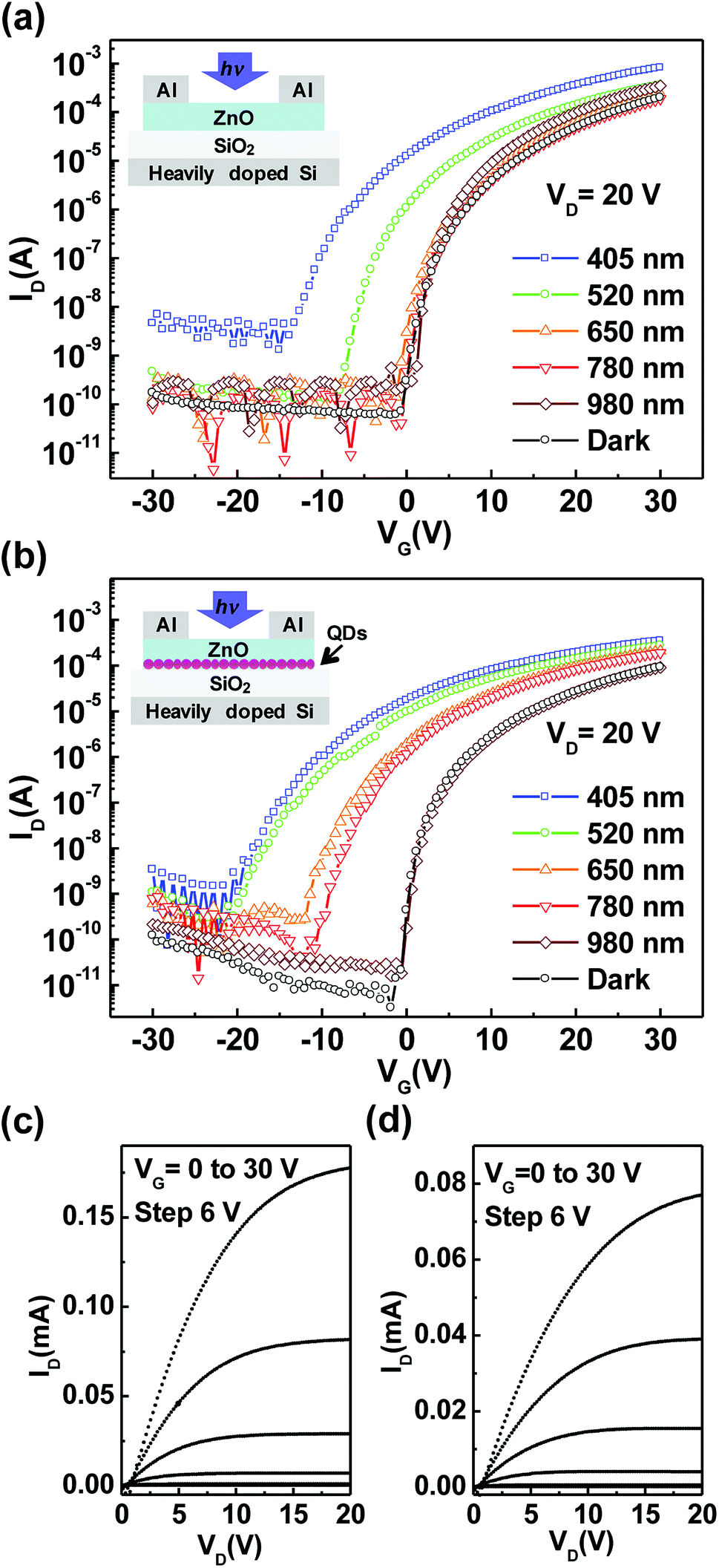 | ||
| Fig. 1 (a) Transfer curves of ZnO TFTs upon exposure to various wavelengths of light (405, 520, 650, 780, 980 and dark). The inset shows the schematic of the ZnO TFTs. (b) Transfer curves of the ZnO TFTs decorated with interfacial QDs as shown in the inset. The drain voltage was set to 20 V during measurement. Output characteristics of (c) ZnO TFTs and (d) ZnO/QDs TFTs. | ||
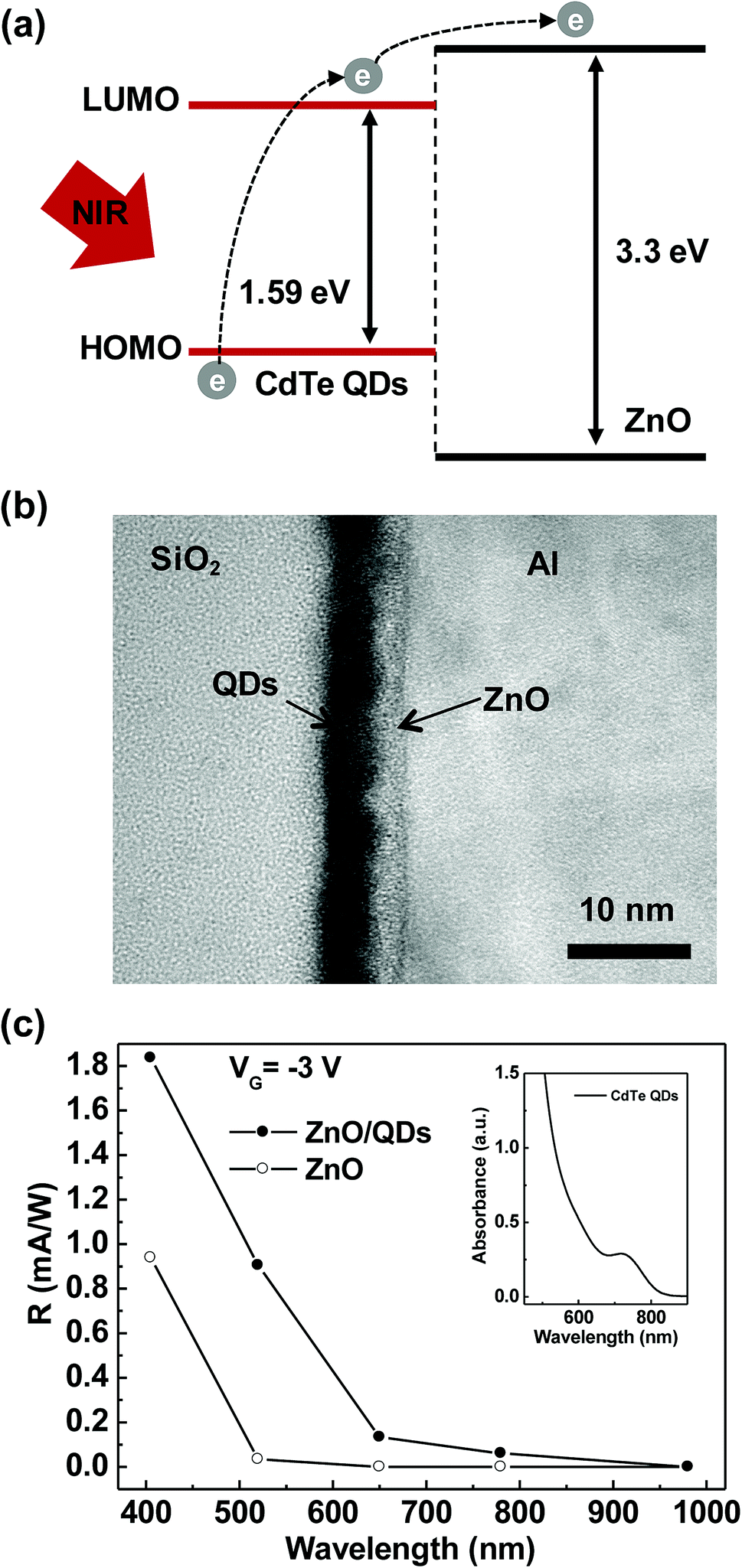 | ||
| Fig. 2 (a) Band diagram of small band-gap QDs and wide band-gap ZnO. (b) Cross-sectional TEM image of the device. (c) Photoresponsivity of ZnO TFTs and ZnO/QD TFTs as a function of the wavelength of exposed light. The gate voltage was kept at −3 V during measurement. The inset shows the absorption spectrum of the QDs. | ||
Here, Itotal is the total current in the device; Idark is the dark current; P is the incident power of the illumination; Apt is the product of channel width and thickness; Apd is the spot size of the laser source; Jph is the photocurrent density; P is the incident laser power density.23 The photoresponsivity was calculated at VG = −3 V as shown in the Fig. 2(c). The photoresponsivity of the ZnO TFTs was negligible with the illumination of low energy photons (λ = 980, 780, 650 and 520 nm), while the photoresponsivity was evaluated as 0.94 mA W−1 when the device was exposed to 405 nm wavelength light. In contrast, the ZnO/QDs TFTs showed 0.06 mA W−1 as a photoresponsivity with the illumination of 780 nm-wavelength light. The responsivity was increased according to illumination with higher photon energy light. The photoresponsivity of the ZnO/QDs TFTs was negligible only when illumination with 980 nm light, due to the smaller photon energy than the band gap of the QDs. The photoresponsivity as a function of wavelength clearly shows that small band gap QDs absorbed NIR light, generated photo-excited electrons, and injected them into the conduction band of ZnO. Therefore, the photocurrent and negative Vth shift were observed as shown in Fig. 1(b). The inset of Fig. 2(c) shows the absorption spectrum of the QDs. Clearly, the QDs absorbed low energy NIR light. Photomodulation of the device was measured using a periodic signal of light (1 Hz). Fig. 3(a) shows the photomodulation of ZnO TFTs with a periodic signal of light at 405 and 780 nm wavelengths. Due to the wide band gap of ZnO, the device can modulate only with the periodic illumination of 405 nm-wavelength light. There was no photoresponse on the ZnO TFTs with periodic illumination of 780 nm light, due to the small photon energy that was not enough to overcome the band gap of ZnO. Meanwhile, the ZnO TFTs decorated with interfacial QDs showed photomodulation characteristics upon the periodic exposure light 780 nm in wavelength as shown in Fig. 3(b). The device was perfectly turned on and off according to the periodic on/off signal of light. The photon energy of 780 nm light was sufficient to overcome the small band gap of QDs, which was inserted between the gate insulator and ZnO film.
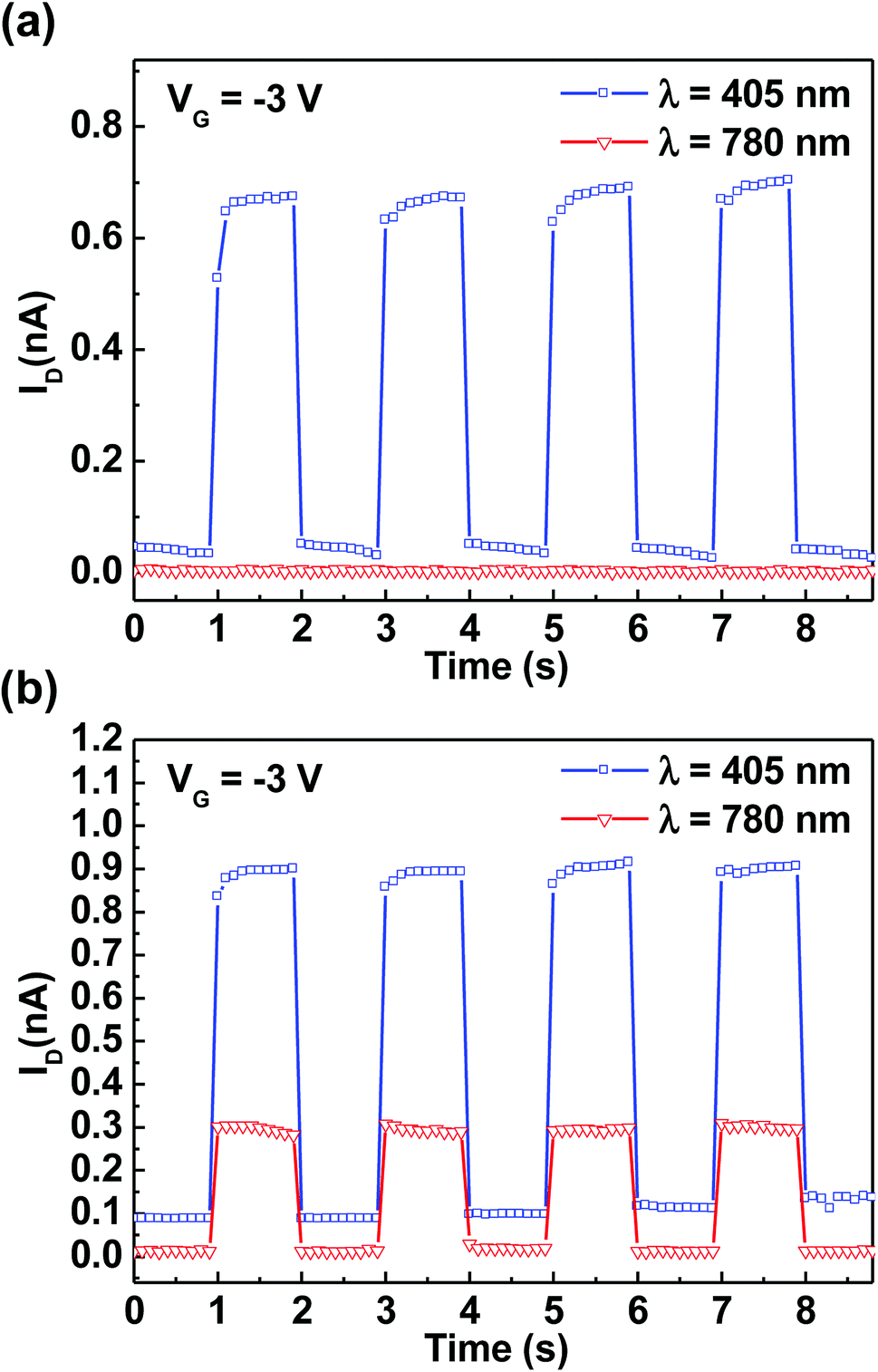 | ||
| Fig. 3 (a) Photoresponse of ZnO TFTs under illumination of a periodic on/off signal from a 405 and 780 nm light source. (b) Photoresponse of ZnO TFTs decorated with interfacial QDs in response to a periodic on/off signal from a 405 and 780 nm light source. The gate voltage was set to −3 V. | ||
A photoinverter circuit was composed of a ZnO/QD TFT and load resistance, as shown in the inset of Fig. 4(a). Considering the working current range of the ZnO/QDs TFTs, the resistance of the load resistor was set to 2 MΩ. The output voltage (Vout) characteristics of the photoinverter circuit was measured as a function of the input voltage (Vin). Typical characteristics of the inverter circuit were measured without exposure to light as shown in Fig. 4(a). The curve was measured again with exposure to 980 and 780 nm wavelength light. With 980 nm-wavelength illumination, the transfer curve did not change, and showed similar inverter characteristics to the curve measured without the light exposure. However, the ZnO/QDs TFTs generated a photocurrent with the exposure of 780 nm light. Therefore, we could observe a negative shift of the inverter curve with the illumination of 780 nm light as shown in Fig. 4(a). The photomodulation of the circuit was measured as shown in Fig. 4(b). The Vout signal was measured with the periodic signal of light, while Vin was set to 10 V. As expected, the photoinverter circuit did not respond to the periodic signal of 980 nm light. On the other hand, the circuit responded to the periodic signal of 780 nm light, as shown in Fig. 4(b), which means that the ZnO/QDs phototransistor could be a basic component from which to build more complicated NIR optoelectronic circuits.
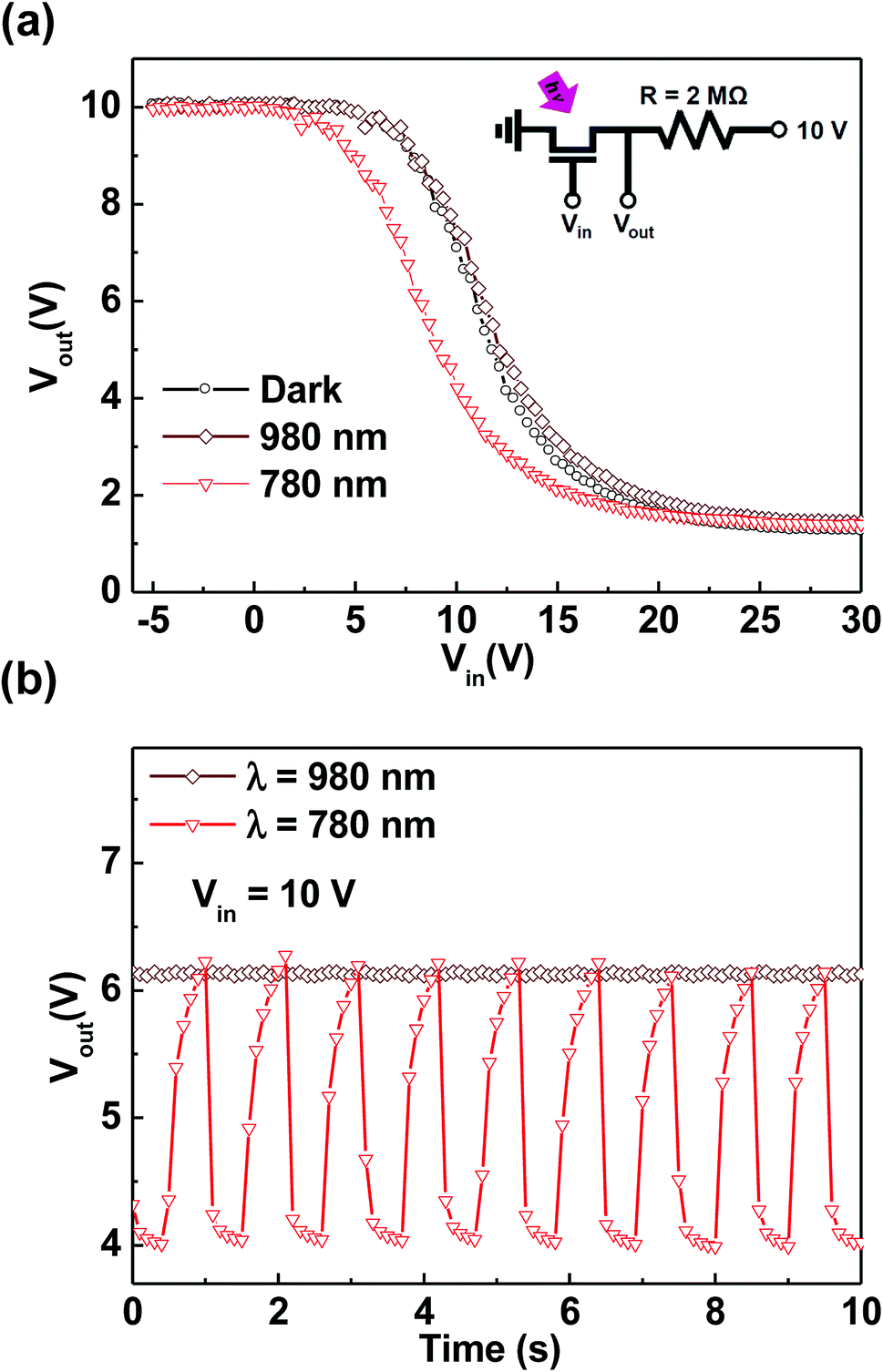 | ||
| Fig. 4 (a) Photo-induced voltage characteristics of a photoinverter consisting of a ZnO/QD phototransistor and load resistor (2 MΩ) illuminated under different wavelengths (780, 980 nm and dark). Inset shows the circuit diagram. (b) Photoswitching characteristics in response to a periodic on/off light signal with 780 or 980 nm wavelength. The Vin was set to 10 V during measurement. | ||
Conclusion
In this study, we fabricated a ZnO/QD TFT that can be modulated by an NIR light signal. Small band gap QDs were inserted in the active channel region of the device to enhance the induced photocurrent with the illumination of NIR light. The photoelectrical characteristics indicated that small band gap QDs can absorb low-energy NIR photons, generate photo-excited carriers, and inject them into the conduction band of ZnO. Therefore, a photocurrent was measured on the device with the illumination of NIR light. The photoresponsivity of the ZnO/QD device was 0.06 mA W−1, while that of the device without QDs was 1.7 × 10⁻⁵ mA W−1 upon exposure to NIR light. In addition, a photoinverter circuit was built that was composed of ZnO/QD TFTs and a load-resistor. The circuit could respond to the periodic NIR light signal. These results suggest a new way to fabricate NIR optoelectronics based on a wide band gap oxide semiconductor. The hybrid structure of the oxide semiconductor and QDs can act as the basic component of highly transparent NIR optoelectronics.Conflicts of interest
There are no conflicts to declare.Acknowledgements
This work was supported by a research project grant from the National Research Foundation of Korea (NRF-2016R1D1A1B03932144). The research was support by the Pioneer Research Center Program through the National Research Foundation of Korea funded by the Ministry of Science, ICT & Future Planning (NRF-2013M3C1A3065033), as well.References
- W. K. Lin, K. C. Liu, S. T. Chang and C. S. Li, Thin Solid Films, 2012, 520, 3079 CrossRef.
- E. Fortunato, P. Barquinha and R. Martins, Adv. Mater., 2012, 24, 2945 CrossRef PubMed.
- S. E. Ahn, S. Park, T. Kim, J. Park and S. Jeon, J. Vac. Sci. Technol., B: Nanotechnol. Microelectron.: Mater., Process., Meas., Phenom., 2015, 33, 031205 Search PubMed.
- J. H. Na, M. Kitamura and Y. Arakawa, Appl. Phys. Lett., 2008, 93, 063501 CrossRef.
- G. J. Lee, J. Kim, J. H. Kim, S. M. Jeong, J. E. Jang and J. Jeong, Semicond. Sci. Technol., 2014, 29, 035003 CrossRef.
- J. S. Park, W.-J. Maeng, H.-S. Kim and J.-S. Park, Thin Solid Films, 2011, 520, 1679 CrossRef.
- I.-C. Chiu and I.-C. Cheng, IEEE Electron Device Lett., 2014, 35, 90 Search PubMed.
- Y. Jin, J. Wang, B. Sun, J. C. Blakesley and N. C. Greenham, Nano Lett., 2008, 8, 1649 CrossRef PubMed.
- S. Lee, Y. Jeong, S. Jeong, J. Lee, M. Jeon and J. Moon, Superlattices Microstruct., 2008, 44, 761 CrossRef.
- Z. Yin, Q. Zheng, S. C. Chen and D. Cai, ACS Appl. Mater. Interfaces, 2013, 5, 9015 CrossRef PubMed.
- K. Song, J. Noh, T. Jun, Y. Jung, H.-Y. Kang and J. Moon, Adv. Mater., 2010, 22, 4308 CrossRef PubMed.
- A. Pimentel, S. H. Ferreira, D. Nunes, T. Calmeiro, R. Martins and E. Fortunato, Materials, 2016, 9, 299 CrossRef PubMed.
- W. Y. Weng, S. J. Chang, C. L. Hsu and T. J. Hsueh, ACS Appl. Mater. Interfaces, 2011, 3, 162 CrossRef PubMed.
- H. W. Zan, H. W. Hsueh, S. C. Kao, W. T. Chen, M. C. Ku, W. W. Tsai and H. F. Meng, SID Int. Symp. Dig. Tech. Pap., 2010, 41, 1316 CrossRef.
- J. Yu, S. W. Shin, K. H. Lee, J. S. Park and S. J. Kang, J. Vac. Sci. Technol., B: Nanotechnol. Microelectron.: Mater., Process., Meas., Phenom., 2015, 33, 061211 Search PubMed.
- J. Yu, J. E. Cho, H. M. Lee, J. S. Park and S. J. Kang, Jpn. J. Appl. Phys., 2016, 55, 111101 CrossRef.
- S. M. Lee, S. J. Park, K. H. Lee, J. S. Park, S. Park, Y. Yi and S. J. Kang, Appl. Phys. Lett., 2015, 106, 031112 CrossRef.
- X. Liu, X. Yang, M. Liu, Z. Tao, Q. Dai, L. Wei, C. Li, X. Zhang, B. Wang and A. Nathan, Appl. Phys. Lett., 2014, 104, 113501 CrossRef.
- K. S. Cho, K. Heo, C. W. Baik, J. Y. Choi, H. Jeong, S. Hwang and S. Y. Lee, Nat. Commun., 2017, 8, 840 CrossRef PubMed.
- J. E. Cho, J. Yu and S. J. Kang, Curr. Appl. Phys., 2016, 16, 1560 CrossRef.
- A. Rajan, G. Kaur, A. Paliwal, H. K. Yadav, V. Gupta1 and M. Tomar, J. Phys. D, 2014, 47, 425102 CrossRef.
- J. Yu, B. J. Kim, S. Park, I. K. Han and S. J. Kang, Jpn. J. Appl. Phys., 2018, 57, 044001 CrossRef.
- S. W. Shin, K. H. Lee, J. S. Park and S. J. Kang, ACS Appl. Mater. Interfaces, 2015, 7, 19666 CrossRef PubMed.
- P. Pattanasattayavong, S. Rossbauer, S. Thomas, J. G. Labram, H. J. Snaith and T. D. Anthopoulos, J. Appl. Phys., 2012, 112, 074507 CrossRef.
| This journal is © The Royal Society of Chemistry 2018 |