
 Open Access Article
 This Open Access Article is licensed under a Creative Commons Attribution-Non Commercial 3.0 Unported Licence
Highly crystalline Nb-doped TiO2 nanospindles as superior electron transporting materials for high-performance planar structured perovskite solar cells†
Yinhua Lv‡
abc,
Bing Cai‡c,
Qingshan Mac,
Zenghua Wangc,
Jingyue(Jimmy) Liu *ad and
Wen-Hua Zhang*c
*ad and
Wen-Hua Zhang*c
aDalian National Laboratory for Clean Energy, Dalian Institute of Chemical Physics, Chinese Academy of Science, 457 Zhongshan Road, Dalian 116023, China
bUniversity of Chinese Academy of Sciences, No 19(A)Yuquan Road, Shijingshan District, Beijing 100049, China
cSichuan Research Center of New Materials, Institute of Chemical Materials, China Academy of Engineering Physics, 596 Yinhe Road, Shuangliu, Chengdu 610200, China. E-mail: whzhang@caep.cn
dDepartment of Physics, Arizona State University, Tempe, Arizona 85287, USA. E-mail: Jingyue.Liu@asu.edu
First published on 7th June 2018
Abstract
Planar-structured perovskite solar cells (PSCs) have received tremendous attention due to their high power conversion efficiency (PCE), simple process and low-cost fabrication. A compact thin film of electron transport materials (ETMs) plays a key role in these PSCs. However, the traditional ETMs of PSCs, TiO2 nanoparticulate films, suffer from low conductivity and high trap state density. Herein, we exploited TiO2 nanospindles as a compact ETM in planar PSCs for the first time, and achieved an efficient device with a PCE of 19.1%. By optimization with Nb doping into the TiO2 nanospindles, the PCE of the PSC was further improved up to 20.8%. The carrier transfer and collection efficiency were significantly improved after Nb5+ doping, revealed by Mott–Schottky (MS) analysis, space charge limited current (SCLC), photoluminence (PL), time-resolved photoluminence (TRPL) spectra, electrochemical impedance spectra (EIS) and so forth. Moreover, the hysteresis behavior was effectively inhibited and the stability was significantly enhanced. This work may provide a new avenue towards the rational design of efficient ETMs for perovskite solar cells.
Introduction
Over the past few years, organic–inorganic lead halide perovskite solar cells (PSCs) have attracted enormous interest because of their excellent power-conversion efficiencies (PCEs), along with facile fabrication procedures and low material cost.1–3 Within 9 years, the certified PCE of PSCs has been rapidly promoted from 3.8% to 22.7%,4,5 demonstrating enormous potential for future applications. Generally, depending on whether a mesoporous charge transport layer is present or not, the device architectures of PSCs are classified as mesoscopic and planar type. To date, most of the certified high-efficiency PSCs are based on mesoscopic structures, in which a layer of mesoporous metal oxide (such as TiO2, Al2O3, ZrO2, etc.) can act as a scaffold for perovskite to provide a larger interface contact area. However, due to the easier process and lower cost for large-scale fabrication, the planar PSCs received increasing attention and witnessed a rapid development recently.6,7Without a mesoporous scaffold layer, a compact layer of electron transport materials (ETMs) plays a key role in planar structured PSCs to achieve high PV performance.8 The ETMs can extract and transport the photo-generated electrons from perovskite to FTO substrate, and they also can suppress the front-surface recombination. Thus, the crystal phase, morphology, microstructure, conduction band and conductivity of ETM compact layer can significantly affect the PCE of resultant PSCs. To date, various n-typed metal oxide semiconductors, such as TiO2, SnO2, Nb2O5, and ZnO,9–15 have been used as ETMs of PSCs. Among them, TiO2 is the most widely used one.
However, TiO2 film has numerous trap states and suffers from low conductivity and carrier accumulation.16 Further investigation indicates that, metal doping can effectively increase the electrical conductivity of TiO2, and modify the band structure and trap states. For instance, by using yttrium17 doped TiO2 as compact layer, the charge extraction process was improved and the planar PSC device achieved a high PCE of 19.3%. Up to now, magnesium,18 lithium or sodium,19–22 samarium,23 lanthanum,24 tantalum,25 fluorine,26 thallium,27 and other metal28–30 doped TiO2 have been attempted in perovskite solar cells. Niobium-doped TiO2 (Nb:TiO2) has been tremendous used in transparent conductive oxides (TCOs),31 photocatalysis,32,33 lithium and sodium ion batteries,34,35 dye-sensitized solar cells (DSSCs).36–42 However, limited work on Nb:TiO2 has been performed in planar PSCs to date. In 2014, Yang et al.43 synthesized Nb:TiO2 nanorods by adding NbCl5 in the growth process. The Nb:TiO2 nanorods based PSCs had lower series resistance and higher recombination resistance than the undoped ones, and showed a 50% increase in the efficiency (from 4.9% to 7.5%). In 2016, Chen et al. spin-coated a colloid solution containing NbCl5 and titanium(IV) butoxide (TBT) to prepare a 2% Nb:TiO2 film for planar PSCs,44 yielding PCEs up to 16.3%, as a result of the positive shift of flat band potential and the increased conductivity. Similarly, Yin and co-workers reported45 1% Nb:TiO2 thin films via a chemical bath deposition process in a solution containing NbCl5 and titanium chloride, yielding a high PCE of 19.2% under reverse scan and improved stability. However, this kind of amorphous Nb:TiO2 thin film based PSCs showed large I–V hysteresis, for which the PCE under forward scan is only 16.21%. The large I–V hysteresis in the above studies makes it difficult to correctly evaluate the photovoltaics performance of the PSCs.
Herein, we exploited TiO2 nanospindles as the compact ETM in planar PSCs for the first time. Nb5+ was doped in TiO2 nanospindles with a mild and facile one-step solvothermal method. The doping of Nb5+ in TiO2 was confirmed by X-ray powder diffraction (XRD), and X-ray photoelectron spectroscopy (XPS). By optimizing the concentration of Nb5+ ions in the precursor solution, the conductivity and carrier density of the resultant TiO2 compact films can be improved, thus the performance of PSCs can be enhanced. Specifically, the 3% Nb:TiO2 based PSCs can obtain a highest PCE of 20.8% with a slight hysteresis, which is the highest one for Nb:TiO2 based planar PSCs. Further characterizations such as Mott–Schottky (MS) analysis, space charge limited current (SCLC), photoluminence (PL), time-resolved photoluminence (TRPL) spectra, electrochemical impedance spectra (EIS) were carried out to reveal the mechanism behind the improved PV performance caused by Nb5+ doping in detail.
Experimental
Chemicals
The main text of the article should appear here with headings as appropriate. All of the solvents and reagents were used without post-treatment. Acetic acid (Sinopharm Chemical Reagent CO., Ltd), tetra-n-butyl titanate (Kermel), niobium ethoxide (thermoficher scientific, 99.95%) were used as the precursors to synthesis pristine and Nb:TiO2 and terpineol (Aladdin, 95%) and ethanol (Aladdin, 99.8%) were employed to disperse them. FAI, MABr, MACl, and spiro-MeOTAD are all purchased from Xi'an Polymer Light Technology Corp.Synthesis of TiO2 and Nb:TiO2 colloid solution precursors
The main text of the article should appear here with headings as appropriate. The Nb:TiO2 colloid solution was prepared according to our previous report.46 In a typical synthesis, 5 mL tetra-n-butyl titanate was added into 25 mL acetic acid under continuous stirring, with adding proper content niobium ethoxide into the solution according to different molar ratio (0%, 1%, 3%, 5%). Pouring into a 50 mL Teflon-lined stainless steel autoclave after the mixture solution became transparent. The solvothermal reaction was conducted at 200 °C for 24 h. The pristine and Nb:TiO2 colloids were obtained by centrifuged and washed extensively of the precipitate in the autoclave, and stored in absolute ethanol for further use.Fabrication of perovskite solar cells
The main text of the article should appear here with headings as appropriate. FTO glasses were cleaned in ultrasonic bath of water, ethanol, acetone and 2-propanol in sequence, and treated in an O2-plasma cleaner. To prepare TiO2 compact layers (bl-TiO2), as-made pristine and Nb5+-doped TiO2 colloids was mixed with terpineol, and deposited on the bl-TiO2 by spin-coating at 6000 rpm, followed by annealing at 520 °C for 1 h. The thickness of the compact layers could be adjusted by the volume of added terpineol and the spin-parameters such as spin and accelerate speed. After the post-treatment with 40 mM aqueous TiCl4 solution at 70 °C for 40 min and sintering at 520 °C for 30 min, the perovskite films were deposited on the treated TiO2 samples by a two-step spin-coating process. First, 1.3 M of PbI2 in (DMF![[thin space (1/6-em)]](https://www.rsc.org/images/entities/char_2009.gif) :DMSO = 9.5:0.5 v/v) was spin coated onto TiO2 at 1500 rpm for 30 s, and then annealed at 70 °C for 1 min, after PbI2 had cooled down to room temperature, the mixture solution of FAI:MABr:MACl (60 mg:6 mg:6 mg in 1 mL IPA) was spin coated onto the PbI2 at 1350 rpm for 30 s, and a thermal annealing of 150 °C for 15 min in ambient air condition (30–40% humidity) was processed. The HTM was then deposited by spin coating at 5000 rpm for 20 s. The spincoating formulation was prepared by dissolving 72.3 mg spiro-MeOTAD, 28.8 mL 4-tert-butylpyridine, 17.5 mL of a stock solution of 520 mg mL−1 Li-TFSI in acetonitrile and 29 mL of a stock solution of 300 mg mL−1 cobalt(III) salt (FK209) in acetonitrile in 1 mL chlorobenzene (CB). Finally, 80 nm of gold top electrode was thermally evaporated under high vacuum.
:DMSO = 9.5:0.5 v/v) was spin coated onto TiO2 at 1500 rpm for 30 s, and then annealed at 70 °C for 1 min, after PbI2 had cooled down to room temperature, the mixture solution of FAI:MABr:MACl (60 mg:6 mg:6 mg in 1 mL IPA) was spin coated onto the PbI2 at 1350 rpm for 30 s, and a thermal annealing of 150 °C for 15 min in ambient air condition (30–40% humidity) was processed. The HTM was then deposited by spin coating at 5000 rpm for 20 s. The spincoating formulation was prepared by dissolving 72.3 mg spiro-MeOTAD, 28.8 mL 4-tert-butylpyridine, 17.5 mL of a stock solution of 520 mg mL−1 Li-TFSI in acetonitrile and 29 mL of a stock solution of 300 mg mL−1 cobalt(III) salt (FK209) in acetonitrile in 1 mL chlorobenzene (CB). Finally, 80 nm of gold top electrode was thermally evaporated under high vacuum.
Characterizations
The crystalline of synthesized pristine and Nb:TiO2 nanoparticles were examined by XRD measurement performed on a D8 X-ray diffractometer (X' pert Pro-1), employing Cu Kα as incident radiation. The crystal structure and morphology of the products were characterized by transmission electron microscope (TEM; JEOL, JEM-2100, 200 kV) equipped with an EDS spectrometer (Oxford). Surface and sectional morphologies were obtained by scanning electron microscopy, operated at an accelerating voltage of 5 kV (Hitachi S5200). UV-Vis absorption spectra of all samples were carried out on an Evolution™ 201 spectrophometer (Thermo fisher scientific Corporation). Photovoltaic performance was measured using a Keithley digital source meter (Model 2400), under illumination of a simulated sunlight (AM 1.5, 100 mW cm−2) provided by a solar simulator (Enlitech) with an AM 1.5 filter. A metal aperture of 0.09 cm2 was used during the measurement to define the active area of the device and avoid light scattering through the sides. The incident photon-to-current efficiency (IPCE or EQE) was measured in AC mode on a QE-R3011 testing system (Enlitech) with a tungsten–halogen lamp as light source. The monochromatic light intensity for EQE efficiency was calibrated with a reference silicon photodiode. The PL measurement was conducted with time-correlated single photon counting (TCSPC) with a 508 nm laser (DD-510L, Deltaflex, Horiba). Tafel and J-V plots of the electron-only devices were characterized by Keithley 2400 Source in dark. The SCLC, EIS and Mott–Schottky plot were obtained by using a multi-channel potentiostat (VMP3, Biologic) under dark conditions. For the Mott–Schottky analysis, the electrodes were submerged in a 0.1 M KCl aqueous solution, with a Pt counter electrode and Ag/AgCl reference electrode. The values were recorded at frequency of 80 mHz. EIS datas were recorded at 0 and 0.8 V in the frequency range from 1 MHz to 100 mHz with an AC amplitude of 30 mV. The Mott–Schottky datas were recorded at the frequency of 80 mHz in the applied voltage range from −1.0 V to 0 V with an AC amplitude of 30 mV.Results and discussion
Fig. 1a shows the X-ray diffraction (XRD) patterns of the pristine and Nb:TiO2 with different doping levels. All diffraction peaks of the samples can be assigned to the anatase phase (PDF: 01-084-1286). Fig. S1† presents the Raman spectra of the pristine and 3% Nb:TiO2, which are almost the same. The peaks at 144, 397, 515 and 640 cm−1 are clearly observed, matching well with the modes of anatase TiO2, which further confirms that the anatase nanocrystalline structure is retained after Nb5+ doping. In addition, the (101) anatase peaks (Fig. 1b) show a slight shift to a lower diffraction angle with increasing niobium concentration because of the larger radius of Nb5+ (0.64 Å) compared to that of Ti4+(0.61 Å). Furthermore, a gradually and slightly broadened FWHM (full width at half maximum) of XRD in Fig. 1b suggest that the crystallite sizes decrease with increased the niobium contents, which can be inferred from the Debye–Scherrer equation.40 | ||
| Fig. 1 (a) XRD patterns of the pristine TiO2 and Nb:TiO2; (b) the magnified XRD patterns for the (101) plane; (c and d) XPS spectra of TiO2 and 3% Nb5+-doped for Ti and Nb states respectively. | ||
To confirm the inclusion of Nb element in TiO2 nanospindles, the energy-dispersive spectroscopy (EDS) and X-ray photoelectron spectroscopy (XPS) analysis were carried out. The quantitative analysis of Nb5+ contents by EDS is almost in agreement with the theoretical values, as shown in Fig. S2.† The surface chemical composition and the chemical states of the sample with 3% Nb:TiO2 were analyzed by XPS as presented in Fig. 1c and d. The characteristic peaks of Ti4+ 3d5/2 and Ti4+ 3d3/2 (464.4 eV and 458.7 eV) were similar in pristine and 3% Nb:TiO2 without any shift, indicating that no Ti3+ and Ti2+ existed in both samples. Two peaks with binding energies of 209.8 and 207.0 eV are assigned to the 3d5/2 and 3d3/2 of Nb5+. The atomic concentration of Nb in the doped sample was estimated to be 2.1 atom% by XPS, which is a little lower than that from the EDS. This may be due to the fact that XPS is a surface-sensitive analysis tool and can only detect the informations in 1–2 nm of the surface. Combined with the results of EDS and XPS, Nb element was successfully doped into the TiO2 nanostructures.
The morphologies of the pristine TiO2 and the 3% Nb:TiO2 TiO2 samples are shown in Fig. 2(a–d). All samples exhibited uniform and narrow size distribution (Fig. S4†). Additionally, the particle size decreases with increasing the amount of Nb precursor, which is consistent with the slightly broader FWHM of XRD in Fig. 1b. The pristine TiO2 is spindle-shaped (Fig. 1a and c), and doping ions with larger radius (Nb5+) changes the aspect ratio by reduction along the c-axis.47 The mean sizes and shapes of the Nb:TiO2 spindles changed slightly in comparison with that of the undoped one when the doping concentration varied from 1% (Fig. S5a and b†) to 3% (Fig. 2b and d). While for the one, a significant morphological change happens for 5% Nb:TiO2 system (Fig. S5c andd†). HRTEM in Fig. 2c and d demonstrate the highly crystalline nature for both samples.
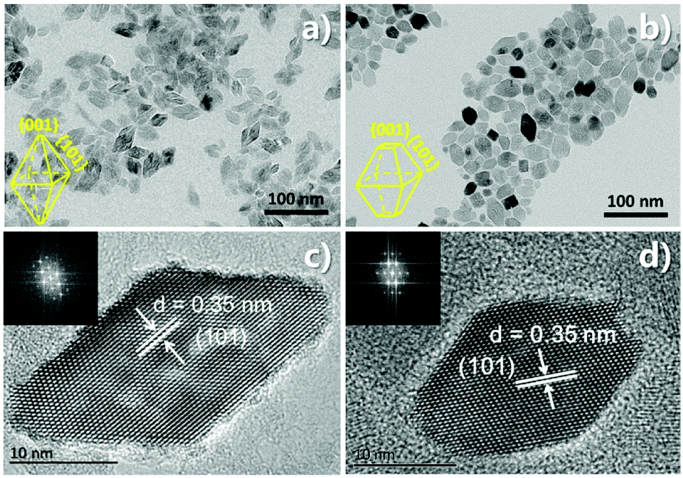 | ||
| Fig. 2 TEM (a and b) images and HRTEM (c and d) images of the pristine TiO2 nanoparticles (left) and 3% Nb:TiO2 nanoparticles (right), respectively. | ||
A thin layer of 35 nm Nb:TiO2 film was used as ETLs for the n–i–p PSCs with a planar structure (FTO/bl-Nb:TiO2/(FAPbI3)x(MAPbBr3)1−x/spiro-OMeTAD/Au) (Fig. 3a). Fig. S6† shows the atomic force microscope (AFM) images for the bare FTO, pristine and 3% Nb:TiO2 thin films deposited on the FTO substrate. Both of them show dense and compact grains in all the thin films without significant voids. The root mean square (RMS) roughness value of FTO is 10.6 nm, which gradually decreases to 8.53 and 8.23 nm after depositing pristine and Nb:TiO2 nanocrystals, respectively. With coating a layer of TiO2 film, the substrate become much more uniform and smoother, indicating that the TiO2 layers have been successfully coated on the FTO, which is in favor for the deposition of uniform perovskite films. A two-step spin coating method was used to deposit the perovskite layer according to a reported process incorporated with modification.48 The obtained perovskite film was showed in Fig. 3b. The grain size ranging from 300 to 1500 nm was observed, together with dense film morphology and a full surface coverage. The film thickness of the perovskite is ∼600 nm (Fig. 3a), which was comparable to the average grain size from Fig. 3b. As a result, most of the photoinduced electrons could be transported across the perovskites layer toward the electrode without crossing the grain boundaries, which is favorable for reducing the recombination loss.
 | ||
| Fig. 3 (a) Cross-sectional SEM image for the Nb:TiO2 based PSC, (b) plane-view SEM image for the (FAPbI3)x(MAPbBr3)1−x perovskite film. | ||
Photovoltaic properties of undoped and doped TiO2-based PSCs (with a 0.09 cm2 aperture) were measured under AM 1.5G conditions (100 mW cm−2). Fig. S7† shows the device performance optimized as a function of Nb doping level; Table S1† displays the corresponding average photovoltaic parameters. It's noteworthy that the PCE increases from 18.6% to 20.4% when the Nb content is changed from 0 to 3%. But the PCE drops to 18.8% when the doping content of Nb in TiO2 is further increased to 5%. It is apparent that there is an optimum Nb content for the device performance at 3%. Fig. 4a shows the J–V curves of the champion devices based on both pristine TiO2 and 3% Nb:TiO2 ETMs. The undoped TiO2 based cells exhibited reverse scanning PCEs of 19.1% (with JSC = 23.2 mA cm−2, VOC = 1.07 V, and FF = 77.0%), and forward scanning PCE of 18.2% (with JSC = 23.2 mA cm−2, VOC = 1.04 V, and FF = 75.3%), showing an obvious hysteresis behavior. In contrast, the best device based on the 3% Nb:TiO2 compact layer present a reverse scanning PCE of 20.8% (with JSC = 23.6 mA cm−2, VOC = 1.13 V, and FF = 78.4%), and a forward scanning PCE of 20.2% (with JSC = 23.5 mA cm−2, VOC = 1.10 V, and FF = 77.8%). The efficiencies are much higher than the pristine counterparts under both scan directions. Moreover, the hysteresis was apparently suppressed due to the Nb5+ doping. Similar results have been reported previously,45 and will be discussed later.
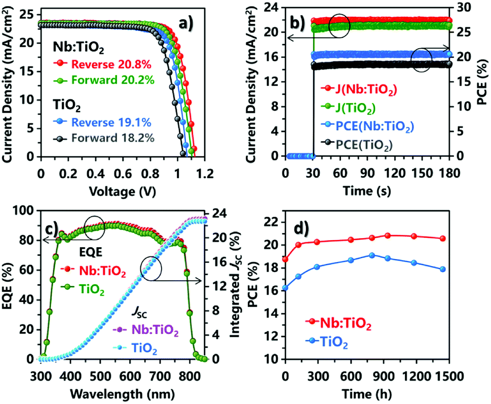 | ||
| Fig. 4 Photovoltaic performance for the PSCs: (a) J–V curves, (b) stabilized current densities and PCEs at maximum power points, (c) external quantum efficiencies (EQEs) (d) stability of unencapsulated PSCs devices with TiO2 and 3% Nb-doped TiO2 as ETLs under air exposure (humidity: 35%, stored in dark) for different time periods. | ||
Additionally, to study the power conversion efficiency under real-world working conditions, we have measured the steady output power for both devices under constant voltage bias at the maximum power-points (0.94 V for Nb:TiO2 and 0.88 V for the undoped TiO2) as plotted in Fig. 4b. It can be seen that the output current density was around 21.9 mA cm−2 for the Nb:TiO2 spindles-based PSCs at steady state after ∼150 s, resulting in a steady output efficiency of 20.6%, which were much better than that of the undoped TiO2 based device (with output current density of 21.2 mA cm−2 and efficiency of 18.7%). To the best of our knowledge, the PCE of 20.6% represents the highest efficiency among the Nb:TiO2 based PSCs reported so far. More data about the optimization of Nb5+ content from 0% to 5% were shown in details in Fig. S7 and S8.† Furthermore, we have also optimized the thicknesses of the Nb:TiO2 films by changing the concentration or the spinning coating parameters. Too thin Nb:TiO2 films (≤35 nm) shows low surface coverage, and is not suitable for use as ETMs of PSCs. The cross-sectional SEM images of the 50 and 80 nm Nb:TiO2 films based PSCs were shown in Fig. S9a and b.† With the increasing of the film thickness, the VOC and FF decreased obviously as a result of the enhanced series resistance and recombination, leading to a decrease of the PCEs as shown in Fig. S9c and d.†
The typical external quantum efficiencies (EQEs) of the devices made from pristine and Nb5+ doped TiO2 compact layers are comparatively shown in Fig. 4c. The photo response edges for both devices locate at ∼820 nm with almost the same shape. In the visible region, the EQEs can reach as high as 91.1% and 90.0% at 560 nm wavelength for the Nb:TiO2 based device and the undoped TiO2 based devices, respectively. The integrated short-circuit current of 23.2 mA cm−2 and 22.8 mA cm−2 matched with the corresponding JSC obtained from the J–V results (in Fig. 4a). The higher EQE and larger JSC of Nb:TiO2 based-device should be ascribed to the higher conductivity caused by Nb5+ doping considering the same UV-vis absorption spectra for the pristine and Nb:TiO2 films (in Fig. S10†), as well as the basically unchanged band gaps in both cases.
The long-term stability of the Nb:TiO2 based PSCs without encapsulation was further investigated, as shown in Fig. 4d for the testing under ambient conditions without encapsulation. At the beginning, PCEs of undoped TiO2 formed devices increased steadily with time and reached a peak value at about 800 h storage, then started to decline obviously with prolonging the storage time. In contrast, the PCE of the Nb:TiO2 based PSCs only increased drastically in the first 100 h, and then saturated and kept basically unchanged for the rest of the testing time (more than 1400 h). It is reported that a critical instability of PSCs arose from the UV light-induced desorption of surface-adsorbed oxygen from TiO2, which may introduce more deep surface traps.49,50 The enhanced stability of the present Nb:TiO2 devices may be due to the reduced trap state density and improved charge transferring at Nb:TiO2/perovskite interface, thereby suppressing the charge accumulation and recombination within the devices.45
To further understand the origin of the improvement in the device performance in the present experiments, Mott–Schottky analysis, Tafel curves, space-charge-limited current (SCLC) model analysis, EIS and PL spectra were conducted. Mott–Schottky analysis was employed to reveal the changes of electronic properties of TiO2 compact layers in this work. As shown in Fig. 5a, both curves have positive slopes, indicating that both TiO2 and Nb:TiO2 are n-type.51 The slope of the fitting linear part (blue line) in the Mott–Schottky curves can be used to deduce the carrier density (Ne)51,52 using eqn (1):53
 | (1) |
 | (2) |
| σ = Neμe | (3) |
 | ||
| Fig. 5 (a) Mott–Schottky plots of TiO2 and Nb:TiO2; (b) Tafel plot of the FTO/TiO2(Nb:TiO2)/Au devices (inset) and (c) the corresponding dark current–voltage (I–V) characteristics; (d) I–V plots for TiO2 and Nb:TiO2 films using the space-charge-limited current (SCLC) model with device structure of Ag/TiO2(Nb:TiO2)/Ag. | ||
As well-known, the band alignment,54 or the difference between the LUMO of perovskite and the quasi-Fermi level (EFermi) of the electron transport layer (ETL),55 have great impact on the VOC of the resultant perovskite solar cells. The quasi-Fermi level (EFermi) of ETL is equal to the voltage in the flat-band state Vfb, which is the external voltage when no band bending occurs and can be deduced from the intersection of the fitting linear part of M – S plot.51 A more positive Vfb means a lower EFermi of TiO2, which is benefit for the injection of photoelectrons between the FTO and ETL. Fig. 4a shows that upon Nb5+ doping, Vfb of TiO2 shifted from −466.3 mV to −446.3 mV. The positive shift has also been found in Nb5+-doped rutile nanorod.56 The increase of 20 mV of Vfb may contribute to the increased VOC in the devices.52,56 Moreover, in the M – S analysis, the depletion zone can be regarded as a bulk resistance from the FTO to the films, and expressed with depletion zone width (W).53,57,58 The narrower the W is, the less the contact resistance is. Similar scenario occurs for the charge extraction at adjacent interfaces of ETMs. The value of W can be obtained from the eqn (4):
 | (4) |
Table S2† indicated that Nb:TiO2 has the narrower W of only 2.67 nm. Therefore, doping of Nb5+ not only have positive effect on the conductivity, but also help improve the charge extraction ability from perovskite layer to TiO2 film.
Meanwhile, the improvement in electrical conductivity of TiO2 could be observed from Tafel and the corresponding J–V plot19,44,59,60 (shown in Fig. 5b and c). The direct conductivity could be estimated from the eqn (5):
| I = σ0AL−1V | (5) |
In order to determine the influence of Nb5+ doping on the electron trap state density in the TiO2 films, we have carried out the dark current–voltage (I–V) analysis using the space-charge-limited current (SCLC) model, as shown in Fig. 5d. At low bias voltage section, the linear relation (blue line) means an ohmic response of the device structure. When the bias voltage exceeded a kink point, the current quickly increased nonlinearly (green line), indicating that the trap-states were completely filled. The value of the kink point, named as trap-filled limit voltage (VTFL), can be calculated according to eqn (6):61,62
 | (6) |
Steady-state photoluminescence (PL) (Fig. 6a) showed a more significant PL quench when depositing the perovskite layer on Nb:TiO2 films than on the undoped TiO2 samples, which could be ascribed to the higher electron mobility of doped TiO2, and lower electron barrier at the interface between TiO2 and perovskite. In addition, the time-resolved photoluminescence (TRPL) spectra of the perovskite films on glass, TiO2 and Nb:TiO2 was displayed in Fig. 6b. The PL decay time and amplitudes are modeled using a bi-exponential eqn (7):
 | (7) |
 | (8) |
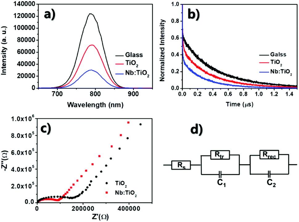 | ||
| Fig. 6 (a) Steady-state photoluminescence spectrum and (b) time-resolved photoluminescence (TRPL) of perovskite deposited on glass (black), undoped TiO2 (red) and Nb:TiO2 (blue), respectively; (c) Nyquist plots of electrochemical impedance spectra (EIS) and (d) equivalent circuit for PSCs based on undoped TiO2 and Nb:TiO2. | ||
The τave of glass/perovskite is 453.7 ns. The average PL decay time for TiO2/perovskite and Nb:TiO2/perovskite were 347.5 and 266.7 ns respectively, indicating that charge transfer in Nb:TiO2/perovskite system was the most efficient. The enhanced charge transfer in Nb:TiO2/perovskite demonstrated that the energy barrier had been reduced, which could be caused by the high mobility and low trap density of the Nb:TiO2 film, resulting in the superior PV performance for the Nb:TiO2-formed PSCs, as discussed in above part (Fig. 2c and d).
To further gain insight into the charge transport process in the devices, electrochemical impedance spectroscopy (EIS) measurements were carried out. Fig. 6c shows an incomplete semicircle in high frequency range, which is assigned to the electron transfer process (Rtr), whereas the main semicircle in the low frequency range is attributed the recombination process (Rrec). The value of series resistance (Rs) is equal to the intercept on the real axis at high frequency range, which is 31.06 and 33.33 Ω for the device for the pristine and 3% Nb:TiO2 ETMs, respectively. Meanwhile, the 3% Nb:TiO2 device possesses a larger semicircle in the low frequency and a smaller semicircle in the high frequency region. The recombination resistance Rrec is associated with the interface charge transport, which increased from 2.08 × 10⁶ Ω for the undoped device to 2.51 × 10⁶ Ω for the 3% Nb-doped device. This clearly confirms the effect of Nb doping on reducing the recombination losses in the devices with Nb-doped TiO2 film. These results confirm that the cell with 3% Nb:TiO2 as ETMs exhibits faster electron transfer and slower recombination.
Conclusions
In summary, Nb5+-doped TiO2 (Nb:TiO2) nanocrystals synthesized via a mild and facile one-step solvothermal method have been successfully used as efficient ETMs in planar PSCs. Doping of Nb5+ increases the conductivity and quasi-Fermi level, eliminates the trap state density, and thus leads to an obvious increase in JSC, VOC and FF of the PSC device. Nb:TiO2 based PSCs exhibited a stabilized PCE of 20.6%, superior to that of the control cell (18.7%), which is among the best level of the Nb:TiO2 formed planar PSCs. Additionally, the Nb:TiO2 based PSCs showed less hysteresis and great long-term stability due to the enhanced electron transport, reduced charge accumulation and trap states. This study demonstrated that Nb:TiO2 nanocrystals show promise for the practical use as superior ETMs of PSCs.Conflicts of interest
There are no conflicts to declare.Acknowledgements
The authors thanked the support from the National Natural Science Foundation of China (Grand No. 21773128), Key Research and Development Projects of Sichuan Province (Grand No. 2017GZ0052), National Postdoctoral Program for Innovative Talents (BX201600138), and Anshan Hifichem Co. Ltd.Notes and references
- H.-S. Kim, C.-R. Lee, J.-H. Im, K.-B. Lee, T. Moehl, A. Marchioro, S.-J. Moon, R. Humphry-Baker, J.-H. Yum, J. E. Moser, M. Graetzel and N.-G. Park, Sci. Rep., 2012, 2, 591 CrossRef PubMed
.
- C. Yang, Y. Wu, Q. Ma and W.-H. Zhang, J. Energy Chem., 2018, 27, 622 CrossRef
- Y. Wu, P. Wang, S. Wang, Z. Wang, B. Cai, X. Zheng, Y. Chen, N. Yuan, J. Ding and W.-H. Zhang, ChemSusChem, 2018, 11, 837 CrossRef PubMed
- W. S. Yang, B.-W. Park, E. H. Jung, N. J. Jeon, Y. C. Kim, D. U. Lee, S. S. Shin, J. Seo, E. K. Kim, J. H. Noh and S. I. Seok, Science, 2017, 356, 1376 CrossRef PubMed
- B. Cai, Y. Xing, Z. Yang, W.-H. Zhang and J. Qiu, Energy Environ. Sci., 2013, 6, 1480 Search PubMed
- Z. M. Zhou, X. Li, M. L. Cai, F. X. Xie, Y. Z. Wu, Z. Lan, X. D. Yang, Y. H. Qiang, A. Islam and L. Y. Han, Adv. Energy Mater., 2017, 7, 1700763 CrossRef
- Y. Z. Wu, F. X. Xie, H. Chen, X. D. Yang, H. M. Su, M. L. Cai, Z. M. Zhou, T. Noda and L. Y. Han, Adv. Mater., 2017, 29, 1701073 CrossRef PubMed
- G. Yang, H. Tao, P. Qin, W. Ke and G. Fang, J. Mater. Chem. A, 2016, 4, 3970 Search PubMed
- M. H. Kumar, N. Yantara, S. Dharani, M. Graetzel, S. Mhaisalkar, P. P. Boix and N. Mathews, Chem. Commun., 2013, 49, 11089 RSC
- Z. Zhu, Y. Bai, X. Liu, C. C. Chueh, S. Yang and A. K. Jen, Adv. Mater., 2016, 28, 6478 CrossRef PubMed
- P. Zhang, J. Wu, T. Zhang, Y. Wang, D. Liu, H. Chen, L. Ji, C. Liu, W. Ahmad, Z. D. Chen and S. Li, Adv. Mater., 2018, 30 Search PubMed
- X. Ling, J. Yuan, D. Liu, Y. Wang, Y. Zhang, S. Chen, H. Wu, F. Jin, F. Wu, G. Shi, X. Tang, J. Zheng, S. Liu, Z. Liu and W. Ma, ACS Appl. Mater. Interfaces, 2017, 9, 23181 Search PubMed
- J. Feng, Z. Yang, D. Yang, X. Ren, X. Zhu, Z. Jin, W. Zi, Q. Wei and S. Liu, Nano Energy, 2017, 36, 1 CrossRef
- X. Ren, D. Yang, Z. Yang, J. Feng, X. Zhu, J. Niu, Y. Liu, W. Zhao and S. F. Liu, ACS Appl. Mater. Interfaces, 2017, 9, 2421 Search PubMed
- D. Yang, R. Yang, J. Zhang, Z. Yang, S. Liu and C. Li, Energy Environ. Sci., 2015, 8, 3208 Search PubMed
- K. Wojciechowski, M. Saliba, T. Leijtens, A. Abate and H. J. Snaith, Energy Environ. Sci., 2014, 7, 1142 Search PubMed
- H. Zhou, Q. Chen, G. Li, S. Luo, T.-b. Song, H.-S. Duan, Z. Hong, J. You, Y. Liu and Y. Yang, Science, 2014, 345, 542 CrossRef PubMed
- H. Zhang, J. Shi, X. Xu, L. Zhu, Y. Luo, D. Li and Q. Meng, J. Mater. Chem. A, 2016, 4, 15383 Search PubMed
- J. H. Heo, M. S. You, M. H. Chang, W. Yin, T. K. Ahn, S.-J. Lee, S.-J. Sung, D. H. Kim and S. H. Im, Nano Energy, 2015, 15, 530 CrossRef
- F. Giordano, A. Abate, J. P. C. Baena, M. Saliba, T. Matsui, S. H. Im, S. M. Zakeeruddin, M. K. Nazeeruddin, A. Hagfeldt and M. Graetzel, Nat. Commun., 2016, 7, 10379 CrossRef PubMed
- X. Li, J. Yang, Q. Jiang, W. Chu, D. Zhang, Z. Zhou and J. Xin, ACS Appl. Mater. Interfaces, 2017, 9, 41354 Search PubMed
- D. Liu, S. Li, P. Zhang, Y. Wang, R. Zhang, H. Sarvari, F. Wang, J. Wu, Z. Wang and Z. D. Chen, Nano Energy, 2017, 31, 462 CrossRef
- Y. Xiang, Z. Ma, J. Zhuang, H. Lu, C. Jia, J. Luo, H. Li and X. Cheng, J. Phys. Chem. C, 2017, 121, 20150 Search PubMed
- H. Li, B. Zheng, Y. Xue, S. Liu, C. Gao and X. Liu, Sol. Energy Mater. Sol. Cells, 2017, 168, 85 CrossRef
- R. Ranjan, A. Prakash, A. Singh, A. Singh, A. Garg and R. K. Gupta, J. Mater. Chem. A, 2018, 6, 1037 Search PubMed
- M. Che, Y. Fang, J. Yuan, Y. Zhu, Q. Liu and J. Song, Int. J. Electrochem. Sci., 2017, 12, 1064 CrossRef
- Q. Cui, X. Zhao, H. Lin, L. Yang, H. Chen, Y. Zhang and X. Li, Nanoscale, 2017, 9, 18897 RSC
- C. Liang, P. Li, Y. Zhang, H. Gu, Q. Cai, X. Liu, J. Wang, H. Wen and G. Shao, J. Power Sources, 2017, 372, 235 CrossRef
- W.-Q. Wu, D. Chen, R. A. Caruso and Y.-B. Cheng, J. Mater. Chem. A, 2017, 5, 10092 Search PubMed
- X. L. Gu, Y. F. Wang, T. Zhang, D. T. Liu, R. Zhang, P. Zhang, J. Wu, Z. D. Chen and S. B. Li, J. Mater. Chem. C, 2017, 5, 10754 RSC
- X. Yang, M.-J. Zhang, Y. Min, M. Xu, Z. Mei, J. Liang, J. Hu, S. Yuan, S. Xiao, Y. Duan, F. Liu, H. Lin, Y. Lin and F. Pan, ACS Appl. Mater. Interfaces, 2017, 9, 29021 Search PubMed
- C. Das, P. Roy, M. Yang, H. Jha and P. Schmuki, Nanoscale, 2011, 3, 3094 RSC
- L. Kong, C. Wang, H. Zheng, X. Zhang and Y. Liu, J. Phys. Chem. C, 2015, 119, 16623 Search PubMed
- D. Bauer, A. J. Roberts, N. Matsumi and J. A. Darr, Nanotechnology, 2017, 28, 195403 CrossRef PubMed
- T. Lan, W. Zhang, N.-L. Wu and M. Wei, Chem.–Eur. J., 2017, 23, 5059 CrossRef PubMed
- S. Parthiban, K. S. Anuratha, S. Arunprabaharan, S. Abinesh and N. Lakshminarasimhan, Ceram. Int., 2015, 41, 205 CrossRef
- M. Yang, D. Kim, H. Jha, K. Lee, J. Paul and P. Schmuki, Chem. Commun., 2011, 47, 2032 RSC
- S. Lee, J. H. Noh, H. S. Han, D. K. Yim, D. H. Kim, J.-K. Lee, J. Y. Kim, H. S. Jung and K. S. Hong, J. Phys. Chem. C, 2009, 113, 6878 Search PubMed
- S. Guo, Y. Horie, S. Imada, M. Z. Bin Mukhlish and T. Nomiyama, J. Mater. Sci.: Mater. Electron., 2017, 28, 13084 CrossRef
- Y. Liu, H. Ran, J. Fan, X. Zhang, J. Mao and G. Shao, Appl. Surf. Sci., 2017, 410, 241 CrossRef
- X. Lue, X. Mou, J. Wu, D. Zhang, L. Zhang, F. Huang, F. Xu and S. Huang, Adv. Funct. Mater., 2010, 20, 509 CrossRef
- W. Liu, H.-g. Wang, X. Wang, M. Zhang and M. Guo, J. Mater. Chem. C, 2016, 4, 11118 RSC
- M. Yang, R. Guo, K. Kadel, Y. Liu, K. O'Shea, R. Bone, X. Wang, J. He and W. Li, J. Mater. Chem. A, 2014, 2, 19616 Search PubMed
- B.-X. Chen, H.-S. Rao, W.-G. Li, Y.-F. Xu, H.-Y. Chen, D.-B. Kuang and C. Su, J. Mater. Chem. A, 2016, 4, 5647 Search PubMed
- G. Yin, J. Ma, H. Jiang, J. Li, D. Yang, F. Gao, J. Zeng, Z. Liu and S. F. Liu, ACS Appl. Mater. Interfaces, 2017, 9, 10752 Search PubMed
- Y. Lv, B. Cai, Y. Wu, S. Wang, Q. Jiang, Q. Ma, J. Liu and W.-H. Zhang, J. Energy Chem., 2018, 27, 951 CrossRef
- L. De Trizio, R. Buonsanti, A. M. Schimpf, A. Llordes, D. R. Gamelin, R. Simonutti and D. J. Milliron, Chem. Mater., 2013, 25, 3383 CrossRef
- Q. Jiang, Z. Chu, P. Wang, X. Yang, H. Liu, Y. Wang, Z. Yin, J. Wu, X. Zhang and J. You, Adv. Mater., 2017, 29, 1703852 CrossRef PubMed
- T. Leijtens, G. E. Eperon, S. Pathak, A. Abate, M. M. Lee and H. J. Snaith, Nat. Commun., 2013, 4, 2885 CrossRef PubMed
- W. Ke, G. Fang, Q. Liu, L. Xiong, P. Qin, H. Tao, J. Wang, H. Lei, B. Li, J. Wan, G. Yang and Y. Yan, J. Am. Chem. Soc., 2015, 137, 6730 CrossRef PubMed
- L. L. K. Gelderman and S. W. Donne, J. Chem. Educ., 2007, 685 CrossRef
- B. Roose, C. M. Johansen, K. Dupraz, T. Jaouen, P. Aebi, U. Steiner and A. Abate, J. Mater. Chem. A, 2018, 6, 1850 Search PubMed
- A. G. R. van de Krol and J. Schoonman, J. Electrochem. Soc., 1997, 144, 1723 CrossRef
- Q. Guo, Y. Xu, B. Xiao, B. Zhang, E. Zhou, F. Wang, Y. Bai, T. Hayat, A. Alsaedi and Z. a. Tan, ACS Appl. Mater. Interfaces, 2017, 9, 10983 Search PubMed
- J. P. C. Baena, L. Steier, W. Tress, M. Saliba, S. Neutzner, T. Matsui, F. Giordano, T. J. Jacobsson, A. R. S. Kandada, S. M. Zakeeruddin, A. Petrozza, A. Abate, M. K. Nazeeruddin, M. Graetzel and A. Hagfeldt, Energy Environ. Sci., 2015, 8, 2928 Search PubMed
- M. Yang, B. Ding and J.-K. Lee, J. Power Sources, 2014, 245, 301 CrossRef
- H. Yu, H. I. Yeom, J. W. Lee, K. Lee, D. Hwang, J. Yun, J. Ryu, J. Lee, S. Bae, S. K. Kim and J. Jang, Adv. Mater., 2018, 30, 1704825 CrossRef PubMed
- T.-S. Su, T.-Y. Hsieh and T.-C. Wei, Sol. RRL, 2018, 2, 1700120 CrossRef
- G. Kakavelakis, T. Maksudov, D. Konios, I. Paradisanos, G. Kioseoglou, E. Stratakis and E. Kymakis, Adv. Energy Mater., 2017, 7, 1602120 CrossRef
- J. Obrzut and K. A. Page, Phys. Rev. B, 2009, 80, 195211 CrossRef
- R. H. Bube, J. Appl. Phys., 1962, 33, 1733 CrossRef
- D. Yang, X. Zhou, R. Yang, Z. Yang, W. Yu, X. Wang, C. Li, S. Liu and R. P. H. Chang, Energy Environ. Sci., 2016, 9, 3071 Search PubMed
Footnotes |
| † Electronic supplementary information (ESI) available. See DOI: 10.1039/c8ra03559h |
| ‡ These authors contributed equally to this work. |
| This journal is © The Royal Society of Chemistry 2018 |