
 Open Access Article
 This Open Access Article is licensed under a Creative Commons Attribution-Non Commercial 3.0 Unported Licence
Improvement of the long-term stability of ZnSnO thin film transistors by tungsten incorporation using a solution-process method
Xiang Yanga,
Shu Jianga,
Jun Li b,
Jian-Hua Zhanga and
Xi-Feng Li*a
b,
Jian-Hua Zhanga and
Xi-Feng Li*a
aKey Laboratory of Advanced Display and System Applications of Ministry of Education, Shanghai University, Shanghai 200072, China
bCollege of Materials Science and Engineering, Shanghai University, Shanghai 200072, China
First published on 7th June 2018
Abstract
In this paper, W-doped ZnSnO (WZTO) thin films and TFT devices are successfully fabricated by a wet-solution technique. The impact of W doping on the film structure, surface morphology, optical properties and chemical compositions of ZTO thin films is analyzed by atomic force microscopy, X-ray diffraction, UV-visible spectroscopy and X-ray photoelectron spectroscopy. The results show that the WZTO thin films have a smooth surface, amorphous structure and fewer oxygen vacancies with increasing W levels. The oxygen vacancy concentration of WZTO thin films is reduced from 40% to 27% with W incorporation. Compared with films free of W doping, for example ZnSnO TFTs, the positive bias stress stability of WZTO TFTs and long-term stability in air are improved obviously and the shift of the threshold voltage (VT) is restrained about six times. The critical reason for the improvement of the ZTO TFT properties is attributed to W-doping, wherein the suppression of oxygen vacancies by W ions plays a dominant role in changing the performance of ZTO thin films and the stability of TFTs.
1. Introduction
Amorphous oxide semiconductor (AOS) thin film transistors (TFTs) have received significant attention for their application in active-matrix flat panel displays due to their high mobility, excellent stability, and good optical transparency.1,2 Although indium gallium zinc oxide (IGZO) has been the preferred semiconductor oxide and is actively commercialized as a channel layer,3–6 unfortunately, gallium and indium elements are scarce as naturally available resources.6,7 Therefore, non-gallium-based and indium-free compounds such as zinc tin oxide (ZTO) have attracted more widespread attention.7,8 Compared with other indium-free binary compounds, ZTO has emerged as a promising candidate semiconductor due to its high charge carrier mobility and comparable device performance with its counterparts.6–10In spite of the above-mentioned advantages of ZTO TFTs, they seem to suffer from severe bias-stress instability,11,12 and the electron density of the back channel surface is susceptible to H2O and O2 molecules in ambient air.7,13 Recent studies have shown that doping third metal ions into ZTO can solve these issues, for example Nb-doped ZTO,7 Zr-doped ZTO,14 Hf-doped ZTO15 and TI-doped ZTO.16 All of these doping third metal ions can improve the properties of ZTO TFT devices. Compared with these metal ions, W has a higher chemical valence and electronegativity and, according to Takio et al. and Liu et al., doping W into In2O3 can change the properties of TFTs, especially bias-stress instability.17–19 Heo et al. demonstrated that W doped into indium zinc oxide (IZO) can greatly combine with oxygen, which raises the stability of TFTs effectively.20,21 Thus, the stability of ZTO TFTs may be effectively improved by incorporating W into ZTO. According to the Hume-Rothery rules, a dopant is able to replace a host ion if they have similar radii. W ions have a similar radius to Zn and Sn ions. In addition, W ions have a higher ionic potential than those of Zn and Sn. Consequently, doping W ions into ZTO may suppress oxygen vacancies effectively and improve the stability of devices by strengthening the bonds between the metal ions and oxygen ions.22 TFT devices can be prepared by different methods, such as magnetron co-sputtering, pulsed laser deposition and the solution process.23–28 Different from traditional vacuum-based techniques, solution-processed techniques pave a suitable pathway for future lower-cost, simplistic and easily controlled stoichiometry applications.29,30 On the basis of these view points, an investigation of W-doping ZTO thin films and TFTs using the solution process should have great significance.
In this paper, WZTO TFTs using solution process technology are firstly fabricated. The impact of W doping on the WZTO thin films and TFTs is thoroughly investigated. Moreover, the role of W doping in ZnSnO TFT devices is deeply discussed.
2. Experimental
A 0.3 M ZTO precursor was prepared by dissolving Zinc acetate dehydrate (Zn(CH3COO)2·2H2O, Alfa Aesar, 98%) and tin chloride pentahydrate (SnCl4·5H2O, SIGMA, 98%) in 2-methoxyethanol. Monoethanolamine (MEA) as a stabilizing agent was added. The molar ratio of Zn![[thin space (1/6-em)]](https://www.rsc.org/images/entities/char_2009.gif) :Sn was fixed at 7:3. For W-doping, different amounts of tungsten hexachloride (WCl6, Alfa Aesar, 99%) were weighted according to the W molar ratios of 1%, 2% and 3%. The WZTO solution was stirred vigorously in a water bath at 70 °C for 3 h, and then aged for 48 h.
:Sn was fixed at 7:3. For W-doping, different amounts of tungsten hexachloride (WCl6, Alfa Aesar, 99%) were weighted according to the W molar ratios of 1%, 2% and 3%. The WZTO solution was stirred vigorously in a water bath at 70 °C for 3 h, and then aged for 48 h.
WZTO thin films were prepared using the spin-coating method. The solution-processed thin films were spin-coated at 3000 rpm for 45 s. Then they were heated on a hot plate at 150 °C for 15 min and annealed at 200 °C for 30 min to enable a gradual evaporation of the residual solvent. This process was repeated 5 times. At last, the films were annealed at 500 °C in air for 1 hour. TFT devices were fabricated with a bottom-gate-top-contact structure on a p-type Si wafer. 100 nm-thick SiO2 as a gate insulator layer was fabricated on a Si wafer by thermal oxidation. The WZTO solutions were spin-coated on the gate dielectric and dried at 200 °C for 10 min. Subsequently, the device was annealed at 500 °C for 1 hour. Finally, Al electrodes were sequentially evaporated onto the top of the active layer as source/drain electrodes. The TFT channel width was 1000 μm and the length was 50 μm.
Characterization of the thin film surfaces was performed by atomic force microscopy (AFM, Nanonavi SPI-400, SPM), while grazing incidence X-ray diffraction (GIXRD, D/MAX-2550) with a glancing incident angle of 1° was used to identify the phase of the films. The optical transmittance of the WZTO films that were deposited on a glass substrate was measured from 300 to 800 nm, using a Hitachi U-3900H Spectrophotometer. The surface valence states of the films were examined by X-ray photoelectron spectroscopy, which was carried out on a Thermo-VG ESCALAB 250 using an Al Kα monochromated (30 eV pass energy, 500 μm spot size) X-ray source. The carbon 1s peak at 284.8 eV was used as a reference for calibration in the XPS results. TFT ID–VG transfer curves were measured in dark and ambient air conditions using an Agilent 4155C semiconductor parameter analyzer with a probe station (LakeShore, TTP4). The threshold voltage (Vth) was extracted from the ID–VG curves in the saturation region by plotting the square root of the drain current versus the gate voltage. The saturation mobility (μsat) was calculated from the following equation:
 | (1) |
3. Results and discussion
XRD was performed to detect the crystallization of WZTO thin films. Fig. 1 shows the GIXRD patterns of 5-layer WZTO thin films with different amounts of W. No prominent crystallization peaks can be observed from the WZTO thin films, which indicates that the structure of the solution-processed WZTO films is amorphous. The amorphous phase of the WZTO thin films may contribute to the formation of WZTO thin films with smooth surfaces and could be beneficial to the fabrication of large sized oxide TFTs and FPDs.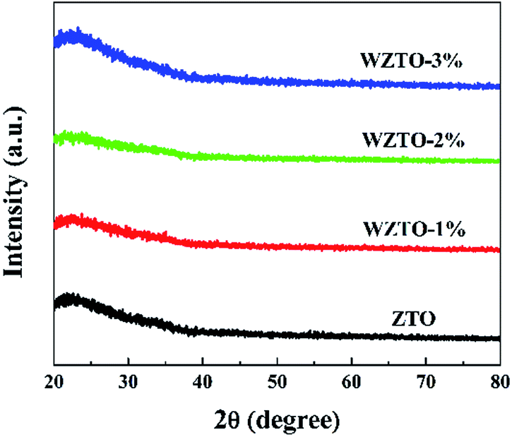 | ||
| Fig. 1 The X-ray diffraction patterns of ZTO and ZTO thin films with different doping levels of W. | ||
AFM images of the WZTO thin films with different W levels are shown in Fig. 2. All of the thin films were annealed at 500 °C. The root-mean-square (RMS) roughness values were calculated from the AFM images. The RMS values for 1%, 2% and 3% mol doped WZTO were 0.28, 0.23 and 0.22 nm, respectively. All of the WZTO films exhibit a homogeneous smooth surface with RMS roughness values less than 1 nm. The RMS roughness of the ZTO thin film was also analyzed (0.93 nm), and was higher than those of the WZTO thin films. This phenomenon reveals that W-doping has a significant effect on film surface morphology. Thus, the addition of W into ZTO thin films would result in smooth surfaces, which should be beneficial to TFT performance through reduced carrier scattering at the dielectric–semiconductor interface.1 The amorphous phase of the WZTO films, which can be derived from the XRD data, may also help to form WZTO films with a smooth surface.
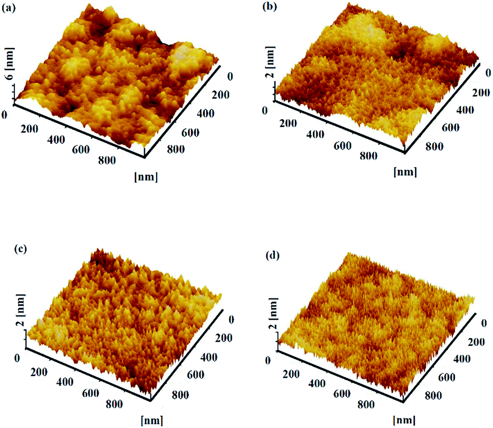 | ||
| Fig. 2 AFM images of undoped ZTO and ZTO thin films with varying doping levels of W, (a) undoped ZTO thin films, (b) 1 at% doped WZTO thin films, (c) 2 at% doped WZTO thin films and (d) 3 at% doped WZTO thin films. | ||
Measuring the optical transmittance of amorphous oxide thin films is a critical technique for indexing. Thus, the optical transmittance properties of WZTO thin films are measured to identify the impact of W doping on the ZTO films, as shown in Fig. 3a. A glass substrate is used as a sample reference during the measurement. All of the WZTO films and the ZTO film have a high transmittance of more than 85% in the visible region, which shows that the effect of W doping on the transparency is of little significance when the content of W is in the range of 1% to 5%. Further addition of W may affect the transparency of the ZTO films, however, the precursor cannot be prepared and becomes slightly turbid when the addition of W reaches 10%. Fig. 3b shows the optical bandgap (Eg) of the ZTO films with different W levels. The following equation is utilized to extract the absorption coefficient of the materials from the transmittance results:
| αhv = constant × (hv − Eg)1/2 | (2) |
 | (3) |
exp[−(EC − EF)/kT], the thermally activated carriers are reduced.31 This implies that W can effectively suppress oxygen vacancies. Therefore, W-doping causes a decrease in carrier concentration.5,32–34
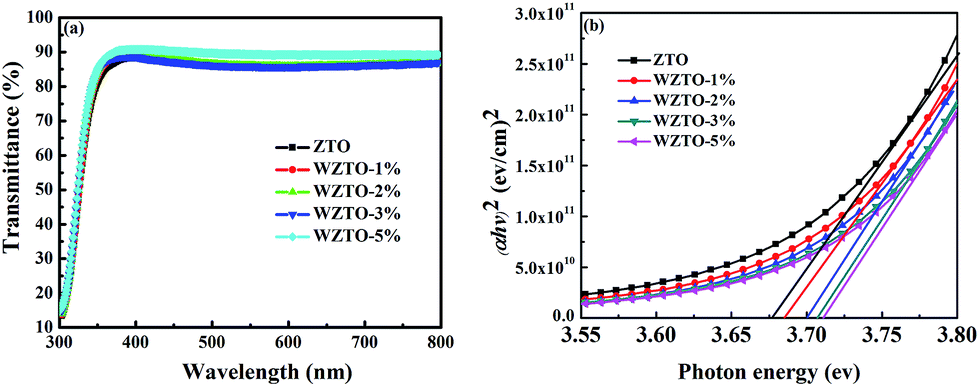 | ||
| Fig. 3 (a) Transmittance spectra of ZTO and ZTO thin films with varying doping levels of W, (b) the optical band gaps of the ZTO films doped with different W%. | ||
To understand the influence of different W levels on the surface chemical bonding states of WZTO thin films, XPS measurements were performed using a sample free of sputter cleaning in order to avoid sputter-induced chemical changes on the surface. All of the binding energies were determined with respect to the adventitious C 1s peak at 284.8 eV. Fig. 4a shows the XPS spectra of W ions for different WZTO thin films, which indicates that W elements can be doped into ZTO successfully. Generally, WZTO semiconductors involve the different charge states of W ions. But, in the WZTO thin films shown in Fig. 4a, the W 4f7/2 peaks all correspond to a binding energy of about 35.4 eV, which reveals that W ions have six ionic charges (W6+) in WZTO films.17,35 Moreover, oxygen 1s (O 1s) XPS spectra for the WZTO films with varying W doping levels are shown in Fig. 4b–e. The XPS O 1s spectra of the WZTO films are deconvoluted into three peaks, 530.1 ± 0.2 eV (OI), 530.9 ± 0.2 eV (OII) and 531.8 ± 0.2 eV (OIII).30 Table 1 lists the oxygen deficiency ratios [i.e. OII/(OI + OII + OIII)] of the WZTO films. It can be seen that the ZTO thin film has a high oxygen deficiency ratio, about 40%. With an increase in W incorporation from 1 to 3 at%, the oxygen vacancy ratio decreases from 40% to 27%. This fact is due to W ions having a strong attractive force with regards to oxygen ions, which can suppress the oxygen vacancies effectively.36 Oxygen vacancies have a substantial effect on the electrical properties and stability under various stresses of TFT applications. Thus, W may be a potential doping element which can remarkably improve the properties of ZTO TFTs.
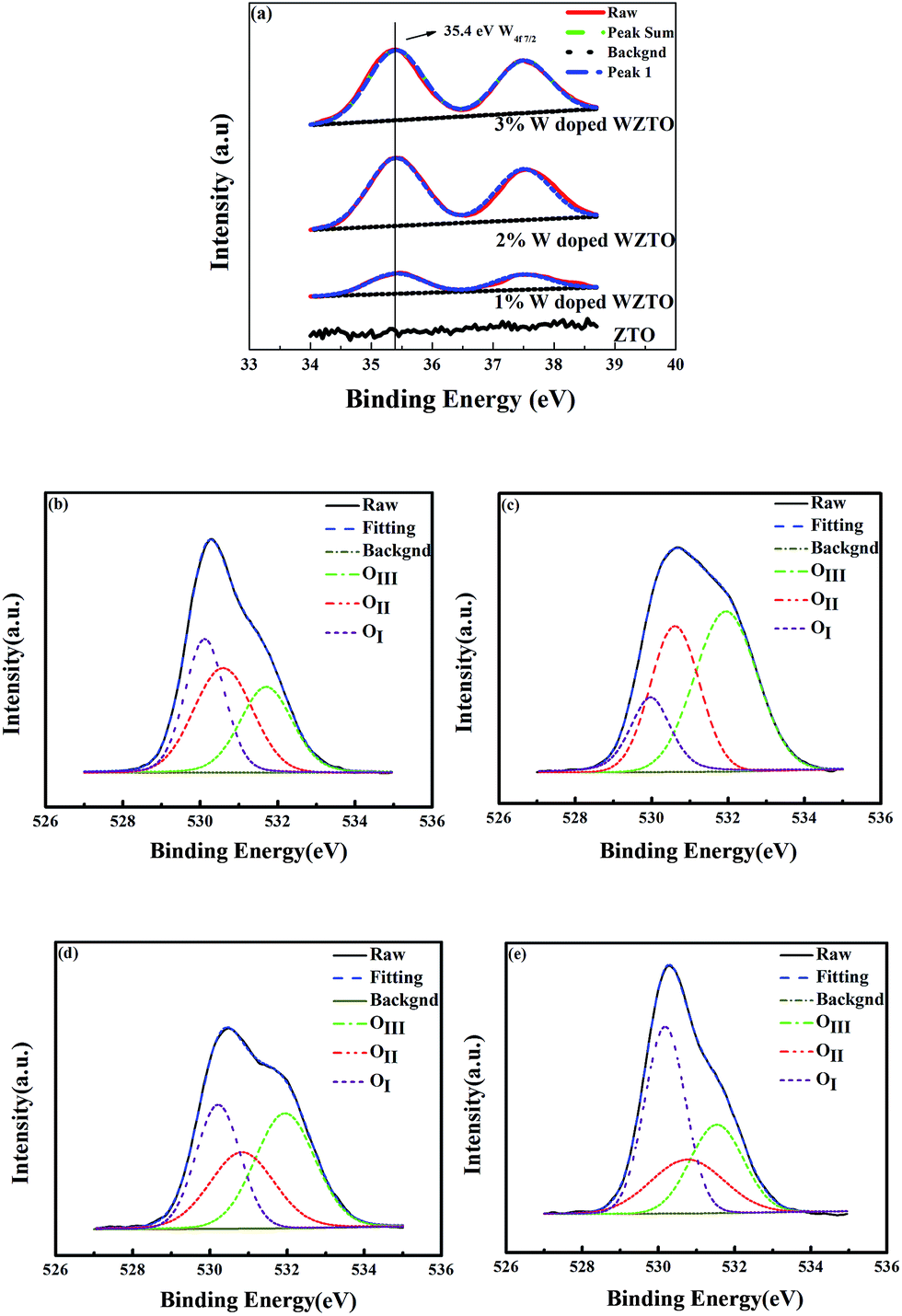 | ||
| Fig. 4 (a) W 4f of the WZTO films, and O 1s XPS spectra of the ZTO thin films with different W levels of (b) 0 at%, (c) 1 at%, (d) 2 at% and (e) 3 at%. | ||
| Device | OII/(OI + OII + OIII) (%) |
|---|---|
| 0% | 40% |
| 1% | 35% |
| 2% | 29% |
| 3% | 27% |
Fig. 5 shows the transfer characteristics of WZTO TFTs with varying W levels. The drain-to-source voltage (VDS) was fixed at 20 V at room temperature, and the gate voltage (VG) varied from −10 to 20 V. The field effect mobility (μ), threshold voltage (VT), subthreshold swing (SS) and ON-state current versus OFF-state current ratio (Ion/Ioff) were extracted according to the transfer curve and are summarized in Table 2. All off currents are defined at VG = −8 V according to the practical applications in the display industry. The μ decreases from 3.7 to 0.5 cm2 V−1 s−1, which shows that the W-doping concentration of the WZTO channel layer has a strong impact on the TFT performance. The on/off current ratios of all of the WZTO TFTs are higher than 106. Moreover, as seen in Table 2, the VT is positive shifted and compared with the ZTO TFT device, the 3 at% WZTO TFT device shows about a 5.3 V shift on VT. The reason for this phenomenon is attributed to the reduction of oxygen vacancies with W-doping which results in a decrease in carrier concentration. Therefore, VT is positive shifted. By increasing the W content to 4 at% and 5 at%, as seen in Fig. 5, the performance of the TFTs deteriorates remarkably. This is because, during excessive W doping in ZTO films, W not only suppresses the oxygen vacancies, but also acts as an interstitial atom and ionized impurity which forms a number of trapping defects and scattering centers, which cause the properties of the devices to decrease.
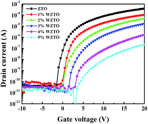 | ||
| Fig. 5 Transfer characteristics of the ZTO TFTs with different W-doping concentrations. | ||
| Device | μ (cm2 V−1 s−1) | Vth (V) | SS (V dec.−1) | Ion/Ioff |
|---|---|---|---|---|
| 0% | 3.7 | 1.75 | 0.33 | 9.5 × 10⁶ |
| 1% | 1.5 | 2.72 | 0.42 | 1.3 × 10⁶ |
| 2% | 1.1 | 5.9 | 0.52 | 1.4 × 10⁶ |
| 3% | 0.5 | 7.05 | 0.58 | 3.5 × 10⁵ |
The positive bias stress (PBS) stability of the TFTs was thoroughly investigated with the increasing W levels. The WZTO TFTs were measured under an effective positive bias stress of 5 V at room temperature for a period of time (0–1200 s). Fig. 6 shows the change in transfer curves as a function of the PBS time for the ZTO, 1 at%, 2 at% and 3 at% doped WZTO devices, respectively. The ZTO TFT exhibits a large positive VT shift of about 3 V with increasing PBS time, but μ, SS and Ion/Ioff show little change. Compared with the ZTO TFT, the WZTO devices show much better stability with an increase in W content. The positive VT (ΔVT) shift of the 1 at% doped WZTO device is about 2 V, the 2 at% doped WZTO device is about 1.5 V and the 3 at% doped WZTO device is about 0.5 V. Generally, the parallel shift of threshold voltage under PBS is attributed to the bulk trap of the WZTO thin films and the interface trap between the gate insulator and the active layer, which are the origins of oxygen vacancies in oxide semiconductors.37 Thus, with an increase in W-doping level, ΔVT decreases significantly. This demonstrates further that W-doping suppresses the oxygen vacancies of ZTO thin films, which is also confirmed by XPS data. This phenomenon is in accordance with the results of ref. 12, 18, and 37–41. Therefore the stability of ZTO TFTs can be improved by W incorporation. The results are similar to W-doped IZO TFTs.21 This further confirms that W is a promising doping element and can effectively improve the stability of ZTO TFT devices.
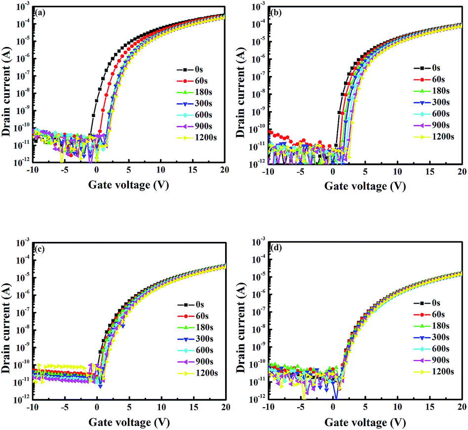 | ||
| Fig. 6 The transfer curve shift included by the effective positive bias stress with varying W doping concentrations. (a) Undoped. (b) 1%. (c) 2%. (d) 3%. | ||
In addition to the study of the PBS of WZTO devices, the long-term air stability of WZTO devices has also been investigated. The transfer curves of the WZTO TFTs are measured after one month of continuous exposure to air. The results are shown in Fig. 7. It was found that the ZTO TFT showed a poor long-term stability at one month with an off current increase from 4.5 × 10⁻¹¹ A to 1.1 × 10⁻⁹ A. With increasing W levels, the off current of the TFTs only slightly increases after being stored under ambient conditions for one month. Compared to other studies about F doped zinc oxide (ZnO) devices, which increase about four orders of magnitude from 10−12 A to 10−8 A, W-doped TFTs show a smaller increase in off current.42 This result indicates that W incorporation into ZTO thin films can effectively improve the long-term air stability of ZTO TFTs and WZTO is a promising candidate active layer material for TFTs.
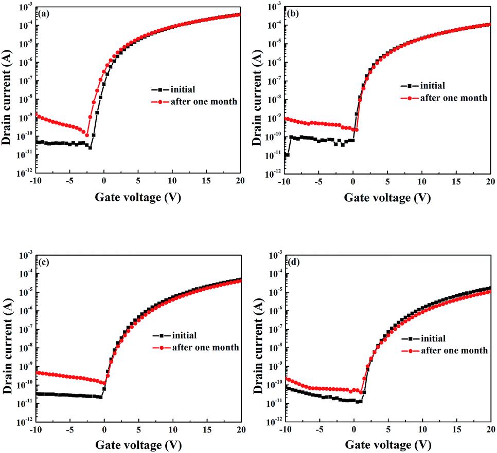 | ||
| Fig. 7 Transfer characteristics of TFTs after storage under ambient conditions. (a) ZTO, (b) 1% WZTO, (c) 2% WZTO and (d) 3% WZTO. | ||
4. Conclusions
W doped zinc tin oxide TFTs were successfully fabricated by the solution process. WZTO films were amorphous and have a smooth surface. All of the WZTO films have a high transmittance above 85% and the optical bandgap shifts towards high photon energy. The oxygen vacancy content decreases from 40% to 27%, which indicates that W incorporation can suppress the oxygen vacancies of ZTO films effectively. In addition, the stability of WZTO TFTs under PBS is optimized obviously, which is attributed to a decrease in oxygen vacancies by W incorporation. Air stability also exhibits a fine influence on the long-term stability of the devices. In summary, WZTO can be fabricated by the solution process and it is a promising candidate channel material for next generation TFT applications.Conflicts of interest
The authors declare no competing financial interests.Acknowledgements
This work is supported by the National Key Research and Development Program of China under Grant no. 2016YFB0401105, the National Natural Science Foundation of China under Grant 61674101 and the Shanghai Science and Technology Commission under Grant 17DZ2291500.References
- Y. N. Gao, J. G. Lu, J. H. Zhang and X. F. Li, J. Alloys Compd., 2015, 646, 675 CrossRef.
- J. H. Zhang, P. P. Dong, Y. N. Gao, C. H. Sheng and X. F. Li, ACS Appl. Mater. Interfaces, 2015, 7, 24103 Search PubMed.
- K. Nomura, H. Ohta, A. Takagi, T. Kamiya, M. Hirano and H. Hosono, Nature, 2004, 432, 488 CrossRef PubMed.
- L. Yue, H. L. Pu, S. J. Pang and Q. Zhang, J. Phys. D: Appl. Phys., 2013, 46, 445106 CrossRef.
- S. M. Park, D. H. Lee, Y. S. Lim, D. K. Kim and M. Yi, Microelectron. Eng., 2013, 109, 189 CrossRef.
- S. Shawn, K. Nico, H. Rudolf, G. Conrad, E. Emre, W. Stefan and J. J. Schneider, ACS Appl. Mater. Interfaces, 2017, 9, 21328 Search PubMed.
- J. S. Jeng, J. Alloys Compd., 2016, 676, 86 CrossRef.
- C. X. Huang, J. Li, C. Y. Zhao, Y. Z. Fu, J. H. Zhang, X. Y. Jiang and Z. L. Zhang, IEEE Trans. Electron Devices, 2016, 63, 11 Search PubMed.
- H. Q. Chiang, J. F. Wager, R. L. Hoffman, J. Jeong and D. A. Keszler, Appl. Phys. Lett., 2005, 86, 013503 CrossRef.
- S.-P. Tsai, C.-H. Chang, C.-J. Hsu, C.-C. Hu, Y.-T. Tsai, C.-H. Chou, H. H. Lin and C.-C. Wu, ECS J. Solid State Sci. Technol., 2015, 4, 176 CrossRef.
- Y. Jeong, C. Bae, D. Kim, K. Song, K. Woo, H. Shin, G. Cao and J. Moon, ACS Appl. Mater. Interfaces, 2010, 2, 611 Search PubMed.
- L. C. Liu, J. S. Chen and J. S. Jeng, Appl. Phys. Lett., 2014, 105, 023509 CrossRef.
- X. Zhang, J. P. Ndabakuranye, D. W. Kim, J. S. Choi and J. Park, Electron. Mater. Lett., 2015, 11, 964 CrossRef.
- Y. S. Rim, D. L. Kim, W. H. Jeong and H. J. Kim, Appl. Phys. Lett., 2010, 97, 233502 CrossRef.
- J. Y. Choi, S. S. Kim and S. Y. Lee, Appl. Phys. Lett., 2012, 100, 022109 CrossRef.
- K. Kishimoto, Y. Nose, Y. Ishikawa, M. N. Fujii and Y. Uraoka, J. Alloys Compd., 2016, 672, 413 CrossRef.
- T. Kizu, S. Aikawa, N. Mitoma, M. Shimizu, X. Gao, M. F. Lin, T. Nabatame and K. Tsukagoshi, Appl. Phys. Lett., 2014, 104, 152103 CrossRef.
- A. Liu, G. X. Liu, H. H. Zhu, B. C. Shin, E. Fortunato, R. Martins and F. Shan, J. Mater. Chem. C, 2016, 4, 4478 RSC.
- S. Aikawa, T. Abatame and K. Tsukagoshi, Appl. Phys. Lett., 2013, 103, 172105 CrossRef.
- B. Y. Oh, J. C. Park, Y. J. Lee, S. J. Cha, J. H. Kim, K. Y. Kim, T. W. Kim and G. S. Heo, J. Solid State Chem., 2011, 184, 2462 CrossRef.
- D. Wan, X. Q. Liu, A. Abliz, C. S. Liu, Y. B. Yang, W. Wu, G. L. Li, J. C. Li, H. P. Chen, T. L. Guo and L. Liao, IEEE Trans. Electron Devices, 2018, 65, 3 CrossRef.
- H. Hosono, J. Non-Cryst. Solids, 2006, 352, 851 CrossRef.
- C. X. Huang, J. Li, Y. Z. Fu, J. H. Zhang, X. Y. Jiang, Z. L. Zhang and Q. H. Yang, J. Alloys Compd., 2016, 681, 81 CrossRef.
- K. B. Park, J. B. Seon, G. H. Kim, M. Yang, B. Koo, H. J. Kim, M. K. Ryu and S. Y. Lee, IEEE Electron Device Lett., 2010, 31, 311 CrossRef.
- W. S. Kim, S. Y. Shin, S. H. Lee, D. S. Han and J. W. Park, Appl. Phys., 2012, 12, S17 Search PubMed.
- J. Y. Bak, S. Yang and S. M. Yoon, Ceram. Int., 2013, 39, 2561 CrossRef.
- J. Sun, W. Yang, Y. Huang, W. Soon Lai, A. Y. S. Lee, C. F. Wang and H. Gong, J. Appl. Phys., 2012, 112, 083709 CrossRef.
- J. Zhang, X. F. Li, J. G. Lu, N. J. Zhou, P. J. Guo, B. Lu, X. H. Pan, L. X. Chen and Z. Z. Ye, RSC Adv., 2014, 4, 3145 RSC.
- Y. L. Xu, X. F. Li, L. Y. Zhu and J. H. Zhang, Mater. Sci. Semicond. Process., 2016, 46, 23 CrossRef.
- X. F. Li, L. Y. Zhu, Y. N. Gao and J. H. Zhang, IEEE Trans. Electron Devices, 2015, 62, 3 CrossRef.
- Y. S. Rim, D. L. Kim, W. H. Jeong and H. J. Kim, Appl. Phys. Lett., 2010, 97, 233502 CrossRef.
- Y. J. Cho, C. A. Nguyen, J. R. Richter, B. H. Ehrstein and J. C. Lee, Appl. Phys. Lett., 2002, 80, 1249 CrossRef.
- D. N. Kim, D. L. Kim, G. H. Kim, S. J. Kim, Y. S. Rim, W. H. Jeong and H. J. Kim, Appl. Phys. Lett., 2010, 97, 192105 CrossRef.
- D. H. Lee, Y. J. Chang, G. S. Herman and C. H. Chang, Adv. Mater., 2007, 19, 843 CrossRef.
- G. A. Niklasson and C. G. Granqvist, J. Mater. Chem., 2007, 17, 127 RSC.
- S. J. Seo, Y. H. Hwang and B. S. Bae, Electrochem. Solid-State Lett., 2010, 13, H357 CrossRef.
- H. Seo, C. J. Park, Y. J. Cho, Y. B. Kim and D. K. Choi, Appl. Phys. Lett., 2010, 96, 232101 CrossRef.
- H. Oh, S. M. Yoon, M. K. Ryu, C. S. Hwang, S. Yang and S. H. K. Park, Appl. Phys. Lett., 2010, 97, 183502 CrossRef.
- C. Y. Zhao, J. Li, D. Y. Zhong, C. X. Huang, J. H. Zhang, X. F. Li, X. Y. Jiang and Z. L. Zhang, IEEE Trans. Electron Devices, 2017, 64, 5 Search PubMed.
- H. Tsuji, M. Nakata, Y. Nakajima, T. Takei, Y. Fujisaki, N. Shimidzu and T. Yamamoto, J. Disp. Technol., 2016, 12, 3 CrossRef.
- N. Mitoma, S. Aikawa, W. O. Yang, X. Gao, T. Kizu, M. F. Lin, A. Fujiwara, T. Nabatame and K. Tsukagoshi, Appl. Phys. Lett., 2015, 106, 042106 CrossRef.
- J. J. Chang, Z. H. Lin, M. Lin, C. X. Zhu, J. Zhang and J. S. Wu, J. Mater. Chem. C, 2015, 3, 1787 RSC.
| This journal is © The Royal Society of Chemistry 2018 |