DOI:
10.1039/C8RA03436B
(Paper)
RSC Adv., 2018,
8, 21968-21974
Interlayer coupling and the phase transition mechanism of stacked MoS2/TaS2 heterostructures discovered using temperature dependent Raman and photoluminescence spectroscopy
Received
21st April 2018
, Accepted 5th June 2018
First published on 14th June 2018
Abstract
Ultrathin 1T (tetragonal)-TaS2 and monolayer MoS2 heterostructures were prepared to study their phase transition (PT) mechanisms and band structure modulation. The temperature dependency of photoluminescence (PL) and Raman spectra was utilized to study interlayer coupling and band structure. The PL results indicate that the band structure of MoS2/TaS2 heterostructures undergoes a sharp change at 214 K. This is attributed to the PT of 1T-TaS2 from a Mott insulator state to a metastable state. In addition, the temperature dependency of the MoS2/TaS2 Raman spectra illustrates that the phonon vibration of the heterojunction is softened due to the effect of interlayer coupling. The present work could provide an avenue to create material systems with abundant functionalities and physical effects.
1 Introduction
2D heterojunctions play an important role in the rich clustering of electronic structures and their optical properties.1–3 Recently, prominent progress in the field of heterojunctions has been made resulting in the development of high speed, performance and power devices.4–6 Atom-thin heterojunctions as a new category of 2D semiconducting material are almost as thin, transparent and flexible as other 2D heterojunctions, with a rich array of new physical phenomena.2–5 At this point, layered two-dimensional (2D) crystals such as transition metal dichalcogenides (TMDCs), graphene and hexagonal boron nitride have attracted noteworthy attention as different 2D materials that can be assembled vertically. Note that TMDCs are a broad family of compounds, which have layered two-dimensional (2D) crystal structures.7–11 They have been recognized as promising materials due to their rich collection of electronic structures and optical properties.12–14 In particular the noteworthy compound MoS2, taken as an example, has a direct band gap in single layer form while multilayers of the same material act as an indirect band gap semiconductor.15 The transition allows for a much enhanced quantum yield of photoluminescence.16 Another typical layered transition metal dichalcogenide (TMD), 1T (tetragonal)-TaS2, displays a sequence of unique structural and electronic phases. At low temperature and ambient pressure, the ground state is the commensurate charge density wave (CCDW) phase. As the temperature increases, it experiences a series of first-order phase transitions to a nearly commensurate (NC) CDW phase at 210 K, to an incommensurate (IC) CDW phase at 350 K, and finally to a metallic phase at 550 K. 1T-TaS2 is an insulator in the C phase, arising from Fermi surface nesting.17–19
Single MoS2 and 1T-TaS2 materials have been widely researched. However, the interlayer coupling and band structures of MoS2/TaS2 heterostructures were rarely studied using Raman and PL spectroscopy. In addition, it was reported that 1T-TaS2 lacked the jump in resistivity that signals transition to the C phase for a few layers or a monolayer of material, or that the C phase was suppressed when the 1T-TaS2 crystals became thinner than 10 nm,20,21 but it was also reported that few-layer 1T-TaS2 remained in the ground state. Therefore, it is still unknown whether ultrathin 1T-TaS2 retains the CC to NC transition and produces an insulating state. Temperature change leads to lattice parameter changes and regulates the band structure, altering the optical properties of the heterojunctions. In addition, it is important to investigate whether the band gap structures of heterojunctions are tuned by the phase transition (PT) of 1T-TaS2. In this work, not only is few-layer 1T-TaS2 studied using temperature dependent Raman spectra and the fitting results used to confirm the PT temperature (from CCDW to NCDW) as 214 K, but also the tuning of large-area 2D heterostructures is reported using chemical vapor deposition (CVD)–grown MoS2 and ultrathin 1T-TaS2 via mechanical exfoliation. In MoS2–TaS2 heterojunctions, interlayer coupling can be tuned externally with temperature variation. Our results also prove that the commensurate CDW remains in the ground state as the thickness of 1T-TaS2 is decreased below 3 nm.
2 Experimental section
2.1 Construction of the heterojunctions
Ultrathin 1T-TaS2 nanosheets were obtained via mechanical exfoliation onto Si/SiO2 (300 nm) from bulk 1T-TaS2 crystals. They were kept in the vacuum chamber to minimize oxidation during the measurement. The bulk 1T-TaS2 crystal was synthesized using chemical vapor transport (CVT) methods.22 A MoS2 monolayer film was grown using a low-pressure CVD (at 30 Pa) technique for 5 minutes. First, the SiO2/Si substrates were cleaned using piranha solution, then placed in the center of the quartz tube’s heating zone and heated to 850 °C in an argon atmosphere to restrict further oxidation. Molybdenum sulfide (MoCl5) powder was loaded in front of the substrates, while sulfur powder was placed in the front of the quartz tube, which was heated to 200 °C. The stacked heterostructure was produced by transferring the monolayer MoS2 film onto the 2.9 nm 1T-TaS2. The as-grown monolayer film MoS2 was coated with a layer of the polymer polymethyl methacrylate (PMMA). The polymer acted as a carrier layer and it was helpful in transferring the MoS2 film. It was spin-coated on the CVD grown monolayer MoS2/SiO2/Si with a speed of 2000 rpm for 15 seconds. The PMMA/MoS2/SiO2/Si material was submerged into potassium hydroxide (KOH) solution. After the PMMA reacted with the KOH, the substrate was taken away. Then the PMMA/MoS2 was transferred into deionized water to remove any residual KOH solution. TaS2/SiO2/Si was put into the water from the side. The system was dried by simply sucking the water droplets away with a paper towel. The PMMA/MoS2 was positioned above the TaS2/SiO2/Si with tweezers. In order to combine the heterostructures better, the sample was baked at 90 °C for 30 min to remove water residue, and then at 120 °C for 30 min to spread the polymer to eliminate possible wrinkles. To dispel the PMMA, the transferred assembly was soaked in propanone for at least 2 hours and the propanone changed several times during this time.
2.2 Material characterization
Temperature dependent Raman scattering and photoluminescence (PL) measurements were carried out using a micro-Raman spectrometer with a Jobin-Yvon LabRAM HR 800 micro-Raman spectrometer and a THMSE 600 heating/cooling stage (Linkam Scientific Instruments) in the temperature range of 77 to 405 K with a resolution of 0.1 K. A laser with a wavelength of 532 nm was used as the excitation source. The laser beam was focused through a 50× microscope with a working distance of 18 mm. The laser power was limited to 10 mW in order to minimize the possibility of sample heating. An air-cooled charge coupled device (CCD) was used to collect the scattered signal dispersed on 1800 grooves per mm grating in the frequency range of 50–450 cm−1. All spectra were rectified by the Bose–Einstein temperature factor to facilitate comparison and eliminate the contribution from the Bose–Einstein population factor. In order to study the variation trend of phonon modes, Raman spectra were fitted with independent damped harmonic oscillators.
2.3 Computational details
The density functional theory (DFT) calculations were executed with plane-wave pseudopotentials from the calculation method of quantum mechanics.23,24 The Perdew–Burke–Ernzerhof generalized gradient approximation (GGA) for the exchange–correlation term was employed for structure optimization and band structure.25 To acquire accurate results for multilayer structures, we incorporated the van der Waals interactions by adding a semi-empirical dispersion potential (D) to the conventional Kohn–Sham DFT energy. The structural parameters can be obtained from DFT-D which is in accordance with the experimental values. A well-converged Monkhorst–Pack k-point set (13 × 13 × 1) was used for the calculation. A conjugate gradient scheme was employed to optimize the geometries until the forces on every atom were 0.005 eV A−1. Geometry optimization was determined using the Broyden–Fletcher–Goldfarb–Shanno (BFGS) minimization technique, with thresholds for the converged structure of energy change per atom smaller than 10−5 eV. The vacuum thickness of a supercell is not smaller than 20 Å and spin–orbit coupling was not included.
3 Results and discussion
3.1 Morphology analysis and the temperature dependent Raman spectra of ultrathin 1T-TaS2
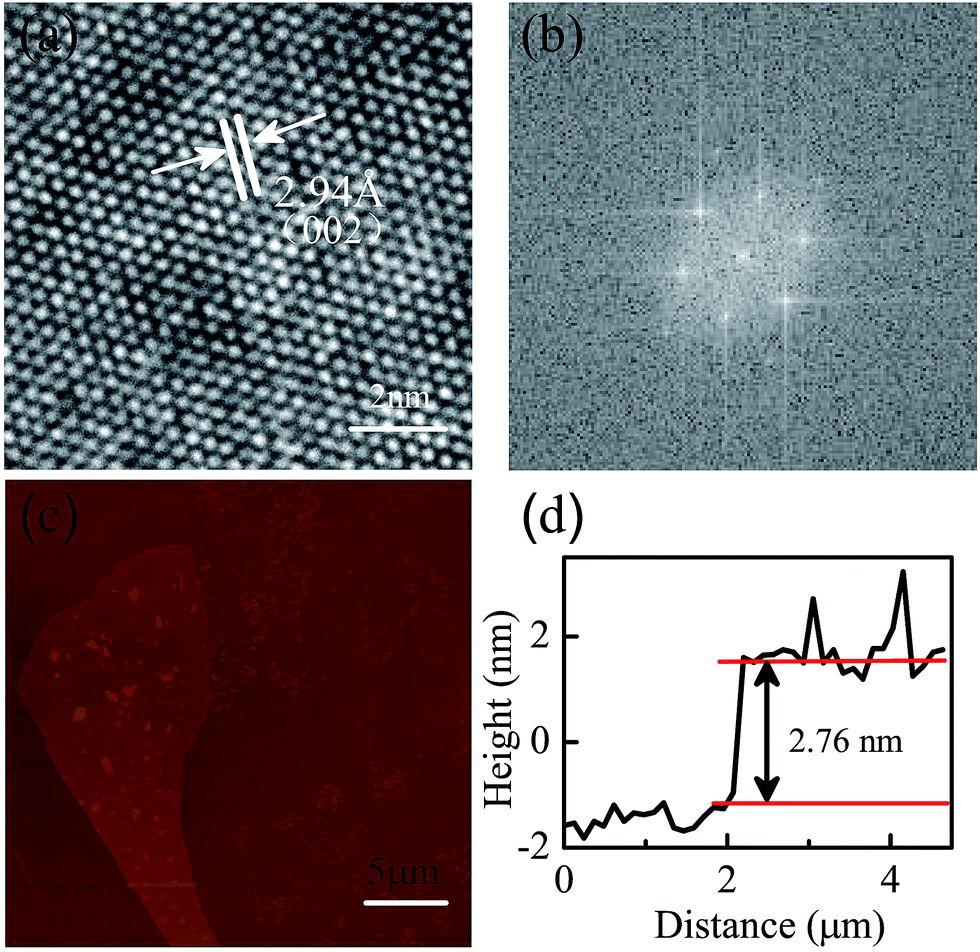
High resolution transmission electron microscopy (HRTEM) was carried out at an accelerating voltage of 200 kV to gain detailed insight into the crystal structure of bulk 1T-TaS2. As shown in Fig. 1(a), the atomic image of bulk TaS2 exhibits the perfect triangular atomic arrangement. The lattice spacing of 2.94 Å is assigned to the (200) plane of 1T-TaS2. Fast Fourier transform (FFT) of the atomic image [Fig. 1(b)] further confirms the tetragonal crystal structure. In addition, the ultrathin 1T-TaS2 topographies [Fig. 1(c)] and height [Fig. 1(d)] (2.76 nm) were investigated via atomic force microscopy (AFM, Dimension Icon, Bruker).
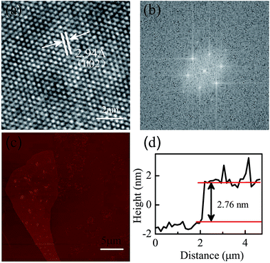 |
| | Fig. 1 (a) A high resolution transmission electron microscopy (HRTEM) image of bulk 1T-TaS2. Panel (b) shows the Fast Fourier transform (FFT) of the atomic image. The (c) AFM image and (d) height profile of few-layer 1T-TaS2. | |
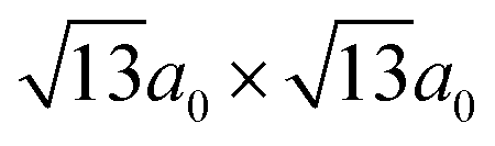
Fig. 2(a) shows the Raman spectra between 50 and 450 cm−1 from a 2.76 nm flake for a series of temperatures during the heating process. All of the features of the Raman spectra at each temperature were in accordance with the results previously reported.26 At low temperature, the phonons’ vibration is intensified and the modes near about 70 cm−1, 86 cm−1 and 105 cm−1 split into explicit peaks. Additional peaks, which appeared in the commensurate CDW state, are due to the folding of the Γ-point modes from the original non-zero wave vector points by the formation of the  superlattice.27,28 At high temperature, some modes in the range of 50–450 cm−1 become weaker gradually and disappear finally, manifesting in the reduction of structural distortion. The modes near 305 cm−1 exhibit a slight redshift with increasing temperature, which can be attributed to the thermal expansion of the lattice and anharmonic phonon–phonon interactions. The modes with a frequency below 140 cm−1 come from the acoustic phonon branches where mainly tantalum atoms move. Those above 220 cm−1 arise from the optical phonon branches where mainly selenium atoms move.27,28 In order to determine the accurate temperature at which the PT (from CCDW to NCDW) takes place, some temperature dependent phonon frequencies are extracted and shown in Fig. 2(b) and (c). There are clear changes in the temperature range of 210–230 K. For example, it can be seen that part of the phonon modes disappears or merges with other modes at the transition from the commensurate to the nearly commensurate phase. The soft Ag-modes located at about 81 cm−1 and 114 cm−1 are particularly noteworthy and undergo severe variations in linewidth and energy, and are marked with stars and triangles in Fig. 2(b).
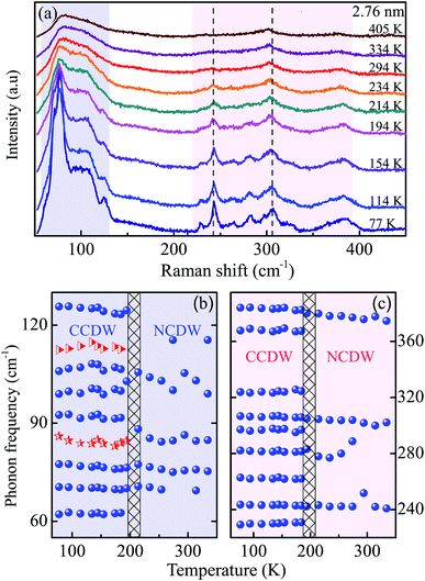 |
| | Fig. 2 (a) Raman spectra of a 2.76 nm-thick flake at different temperatures during the heating process. Temperature dependence of the phonon frequency from the 2.76 nm-thick flake from (b) the low frequency range of 55–130 cm−1 and (c) the high frequency range of 220–390 cm−1. The phase transition (CC–NC) temperature is marked by a dashed line in (b) and (c). | |
3.2 Morphology characteristics and interlayer coupling of the MoS2/TaS2 heterostructure
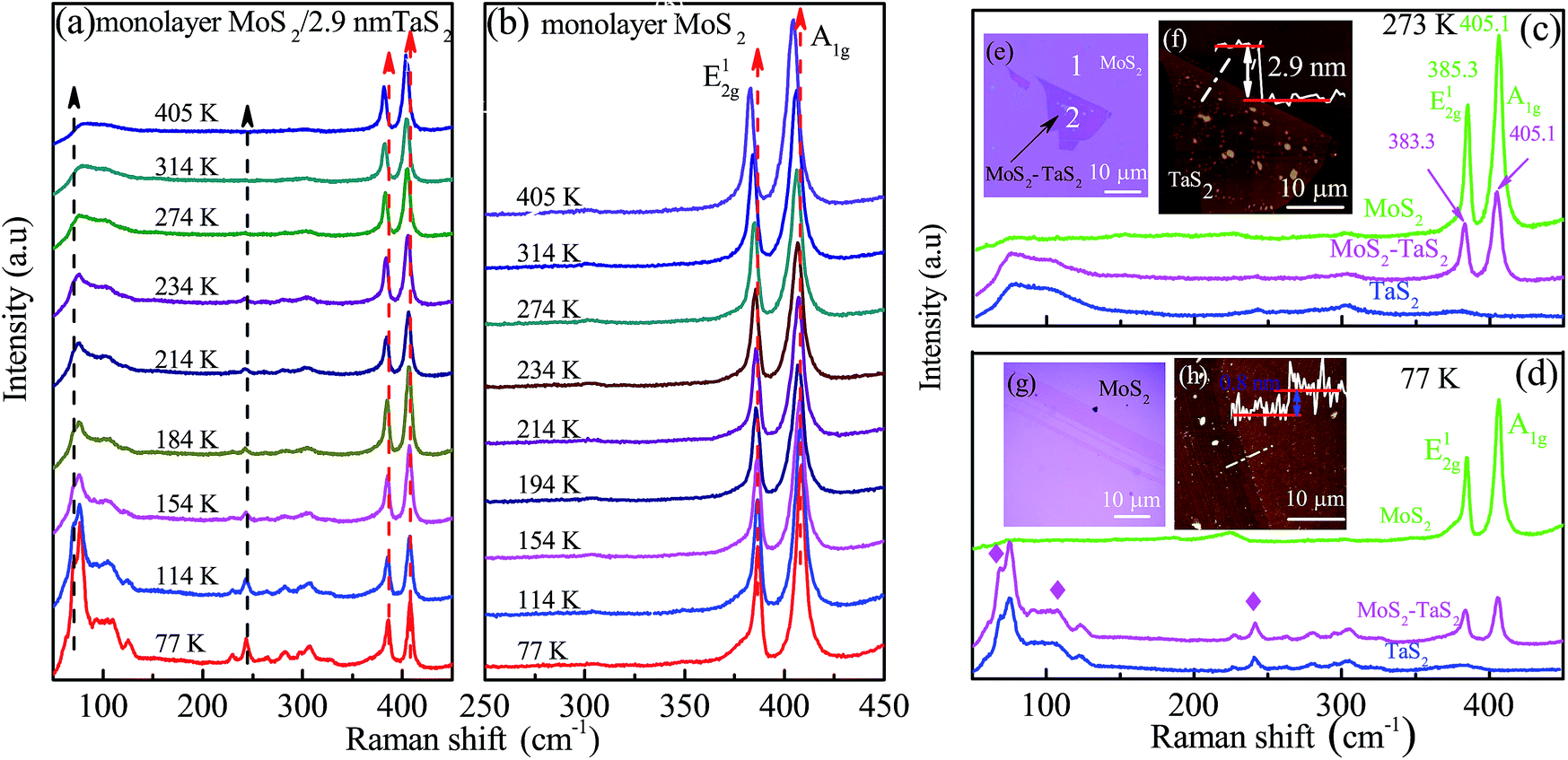
The vertically stacked heterostructure has been investigated using a Raman scattering technique. An optical image of the MoS2/TaS2 heterostructure is shown in Fig. 3(e). It indicates that the MoS2/TaS2 heterostructure has been stacked successfully. The bottom 1T-TaS2 topographies and height (2.9 nm) are displayed in Fig. 3(f). The optical images and topographies of the top MoS2 film are demonstrated in Fig. 3(g) and (h). They indicate that the monolayer MoS2 film was successfully prepared. Fig. 3(a) and (b) show the Raman shift for the MoS2/TaS2 heterostructure and monolayer MoS2, respectively, as a function of temperature. In Fig. 3(b), a downward shift of the MoS2 Raman modes with increasing temperature is shown. This behavior is due to the influence of the anharmonicity and the effect of thermal expansion or volume contribution. As shown in Fig. 3(a), it was found that the E12g and A1g phonon modes from MoS2 are suppressed in the heterostructures, which can be attributed to the softening of the phonon mode by the interlayer coupling of MoS2/TaS2.
 |
| | Fig. 3 Raman spectra of the MoS2/TaS2 heterostructure (a) and monolayer MoS2 (b) at different temperatures during the heating process. Raman spectra of the MoS2, TaS2 and MoS2–TaS2 heterostructures at 77 K (c) and 273 K (d), respectively. (e) An optical microscope image of the MoS2–TaS2 heterostructure. (f) The AFM image and height (2.9 nm) profile of few-layer 1T-TaS2. (g) An optical microscope image of monolayer MoS2. (h) The AFM image and height (0.8 nm) profile of monolayer MoS2. | |
To further explore the effect of interlayer coupling on the heterojunction, we compared the phonon vibration spectrum of MoS2, MoS2/TaS2 and TaS2 at the same temperature. As shown in Fig. 3(c), E12g and A1g phonon modes are located at about 385.3 cm−1 and 405.1 cm−1 for monolayer MoS2 at 273 K. The frequency difference between the E12g and A1g phonon modes is 19.8 cm−1 for the monolayer MoS2 in MoS2/TaS2.29 The Raman mode E12g significantly stiffened by 2 cm−1 and the A1g mode was unchanged in the multilayer MoS2/TaS2 heterostructure, as compared with those in the isolated MoS2 monolayer from Fig. 3(c). This was due to the E12g and A1g modes being sensitive to strain30 and the doping level31,32 in MoS2, respectively. Therefore, the shifted E12g mode and the unchanged A1g mode of MoS2 imply that the strain relaxes differently for MoS2/TaS2 compared to that of MoS2/SiO2, and such a result indicates strong interlayer coupling between TaS2 and MoS2. The Raman spectra of the MoS2–TaS2 heterostructure seem to be a simple superposition of the 2.9 nm TaS2 and monolayer MoS2. At 77 K, these phonon modes (marked with a diamond symbol) split into several well-defined peaks and the mode at 384 cm−1 of TaS2 overlaps the MoS2 E12g Raman modes for the MoS2–TaS2 heterostructure.
3.3 The band structures of monolayer MoS2, few-layer TaS2 and MoS2/TaS2 heterostructures
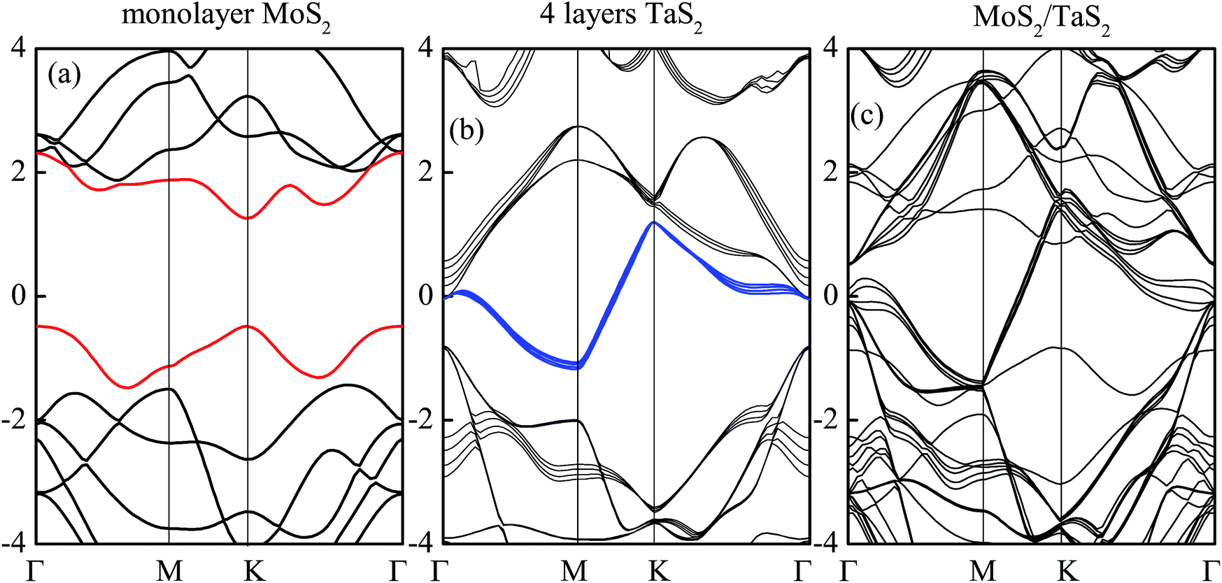
Before the PL spectra of the heterostructure were obtained, we calculated the band structure of monolayer MoS2, 4 layered 1T-TaS2 and their heterojunctions. As shown in Fig. 4(a), the theoretical results show that the bandgap of the MoS2 monolayer is about 1.9 eV. The valance band maximum (VBM) and conduction band minimum (CBM) are located at the K point in the Brillouin zone, which is due to the Mo d-orbitals. The Mo atoms are located in the middle of the S–Mo–S layer sandwiches and are unaffected by interlayer coupling. For the 4 layered 1T-TaS2, the band structure is similar to that of the pristine sample.33 There is a gap of about 0.8 eV below the band crossing Fermi energy (Ef) as shown in Fig. 4(b) and one band crosses the Ef, forming a 2D electron pocket around the M point. In addition, it can be seen that the band diagram of the heterojunction is a combination of the monolayer layer MoS2 and few-layer TaS2, as shown in Fig. 4(c).
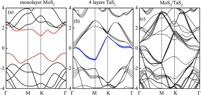 |
| | Fig. 4 The band structures for (a) monolayer MoS2, (b) few-layer TaS2 and (c) MoS2–TaS2 heterostructures. | |
3.4 The transition mechanism of the MoS2/TaS2 heterostructure
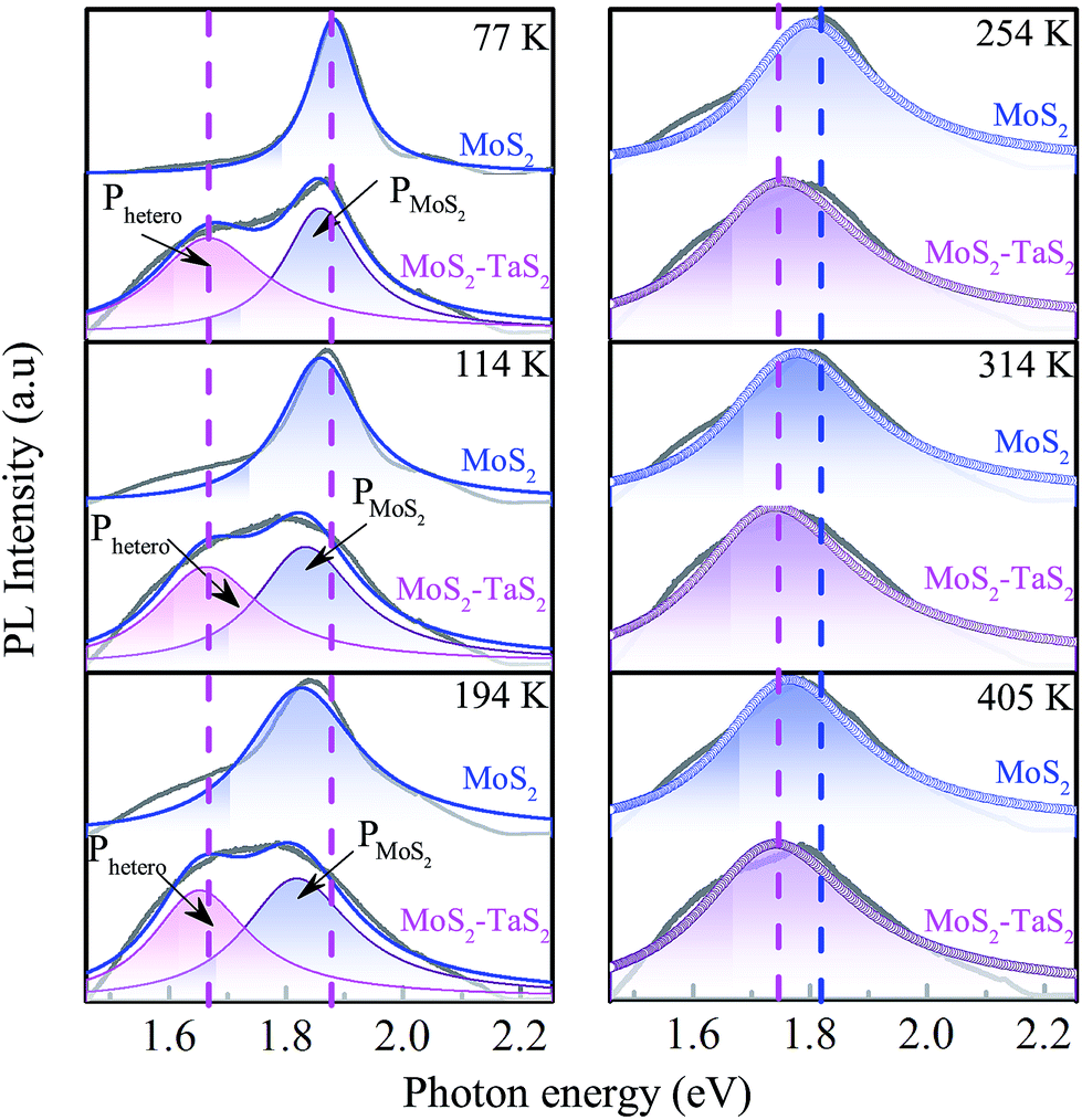
Interlayer interaction is expected to be exponentially sensitive to the interlayer spacing according to tight-binding theory or the quantum tunneling model. To investigate interlayer coupling with different interlayer distances, a variable-temperature tuning process was performed for the monolayer MoS2 and MoS2/TaS2 heterostructures. The PL spectra at 77 K (Fig. 5) collected from the monolayer MoS2 region show a strong peak at a wavelength of about 1.89 eV, which corresponds to the direct excitonic transition energy in monolayer MoS2. However, for the MoS2/TaS2 heterostructure (region 2, Fig. 3(e)), two peaks are observed at about 1.86 and 1.67 eV for 77 K. The peak located at 1.86 eV from MoS2 is marked PMoS2. Another peak located at 1.67 eV was attributed to the direct excitonic transition energies in the top MoS2 and bottom ultrathin TaS2 materials at 77 K. It is marked Phetero. In addition, the MoS2/TaS2 heterostructure forms a type II band alignment.34,35 In the type II heterojunction, the CBM and VBM reside in two separate materials. As shown in the inset schematic diagram of Fig. 6, photoexcited electrons and holes will relax to the conduction band edge of TaS2 when the temperature is varied from 77 K to 214 K. A Phetero peak at about 1.67 eV is observed at 77 K, 114 K and 194 K as shown in Fig. 5, interestingly lying at a lower energy than the peak for the single layers of MoS2 . This suggests that the type II band alignment in the MoS2/TaS2 facilitates the photoexcited electron–hole separation and leads to an enhanced photoswitching performance, as compared to that in MoS2 and TaS2.36 However, the Phetero peak disappears in the MoS2/TaS2 heterostructure when the temperature is beyond 214 K, which is because of the appearance of domain walls. 1T-TaS2 is in the nearly commensurate CDW phase. It also has long been assumed that electron correlations open up a Mott–Hubbard gap in the C phase.37 In addition, electron–electron interactions, electron–phonon coupling, interlayer interactions and disorder could play an important role in this observation. As shown in Fig. 5 (254 K, 314 K and 405 K), the energy band spectra of the MoS2/TaS2 heterostructure is very similar to those of the monolayer MoS2. There is a difference of 14 meV between the monolayer MoS2 and MoS2/TaS2 heterostructure at 254 K, which is owing to the influences of a TaS2 atomic layer for monolayer MoS2. These results show that the ultrathin 1T-TaS2 exhibits abrupt and reversible changes in the lattice structure, which are attractive for device applications.
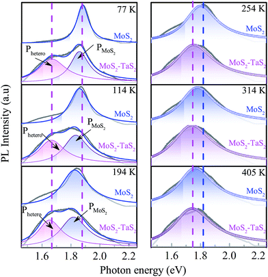 |
| | Fig. 5 PL spectra of MoS2 and MoS2/TaS2 heterostructures at different temperatures during the heating process. | |
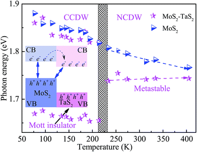 |
| | Fig. 6 PL peak position of the MoS2 and MoS2/TaS2 heterostructures. The inset shows the schematic of the band alignment for the MoS2–TaS2 heterostructure at low temperature. | |
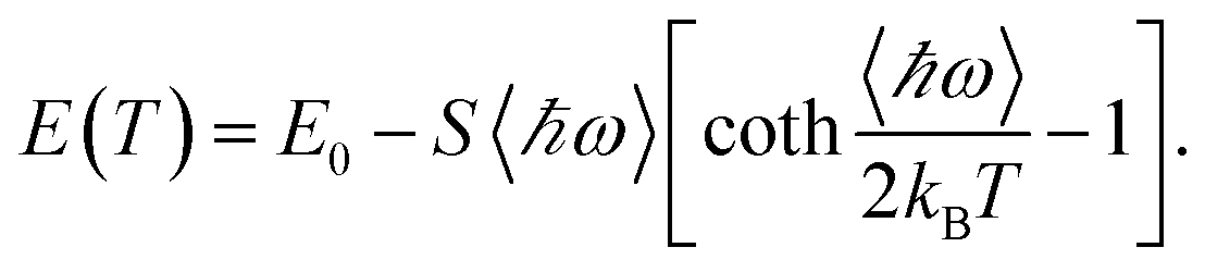
With the purpose of further studying the phase transition mechanism of the MoS2/TaS2 heterojunction, we respectively fit the PL spectra of MoS2 and the MoS2/TaS2 heterojunction to compare their characteristics, as shown in Fig. 6. The redshift of the monolayer from the MoS2 PL peak with an increase in temperature indicates a reduction in the MoS2 energy band gap, which is the energy of the lowest allowed exciton state. In addition, most of the energy gaps of the heterojunction are less than those from MoS2 as shown in Fig. 6. This indicates that the heterojunction regulates the band structure of MoS2, reducing the band gap and increasing the conductivity. The modified Varshni relationship of the band-gap temperature dependence is fitted using the following formula:38,39
| |
 | (1) |
where
E0 represents the emission energy at
T = 0 K,
S is the parameter which describes the coupling strength of an exciton–phonon, 〈
ℏω〉 is an average phonon energy, and
kB and
ℏ are the Boltzmann and Planck constants, respectively. Another phenomena that is evident is that the two PL fitting peaks at low temperature combine into one peak at 214 K. This suggests that the C phase disappears gradually and the NC phase emerges.
4 Conclusions
In summary, the interlayer coupling and phase transition mechanism were studied by variable-temperature spectral experiment. The results of Raman spectroscopy indicate that interlayer coupling causes phonon softening of MoS2/TaS2 heterostructures. It was also found that the MoS2/TaS2 heterostructure forms a type II band alignment. A Phetero peak appears when the TaS2 is located in the C phase. Furthermore, this phenomenon also confirms that commensurate CDW remains in the ground state as the 1T-TaS2 is thinned to 3 nm. These results distinguish the significance of band offsets between different TMDs in tuning the light emission and band structure. It is believed that the analysis method described in our work could be helpful in exploring the interlayer coupling of other similar TMDs.
Conflicts of interest
There are no conflicts to declare.
Acknowledgements
This work was financially supported by the National Key Research and Development Program of China (Grant No. 2017YFA0303403), Natural Science Foundation of China (Grant No. 61674057 and 61227902), Projects of Science and Technology Commission of Shanghai Municipality (Grant No. 18JC1412400, 18YF1407200, 18YF1407000 and 15JC1401600), and the Program for Professor of Special Appointment (Eastern Scholar) at Shanghai Institutions of Higher Learning and the Fundamental Research Funds for the Central Universities.
References
- K. F. Mak, C. G. g. Lee, J. Hone, J. Shan and T. F. Heinz, Phys. Rev. Lett., 2010, 105, 136805 CrossRef PubMed.
- Q. W. Wang, K. Kalantar-Zadeh, K. Andras, J. N. Coleman and M. S. Strano, Nat. Nanotechnol., 2012, 7, 699 CrossRef PubMed.
- T. Yu and M. W. Wu, Phys. Rev. B, 2016, 93, 045414 CrossRef.
- H. Kroemer, Proc. IEEE, 1982, 70, 13 CrossRef.
- B.-S. Kim, D. C. J. Neo, B. Hou, J. Park, Y. Cho, N. Zhang, J. Hong, S. Pak, S. Lee, J. Sohn, H. E. Assender, A. A. R. Watt, S. Cha and J. Kim, ACS Appl. Mater. Interfaces, 2016, 8, 13902 Search PubMed.
- X. Hong, J. Kim, S.-F. Shi, Y. Zhang, C. Jin, Y. Sun, S. Tongay, J. Wu, Y. Zhang and F. Wang, Nat. Nanotechnol., 2014, 9, 682 CrossRef PubMed.
- A. Aruchamy and M. K. Agarwal, Photoelectrochemistry and Photovoltaics of Layered Semiconductors, 1992, vol. 14, p. 1319 Search PubMed.
- S. J. Yun, G. H. Han, H. Kim, D. L. Duong, B. G. Shin, J. Zhao, Q. A. Wu, J. Lee, S. M. Lee and Y. H. Lee, Nat. Commun., 2017, 8, 2163 CrossRef PubMed.
- Z. H. Ji, H. Hong, J. Zhang, Q. Zhang, W. Huang, T. Cao, R. X. Qiao, C. Liu, J. Liang and C. H. Jin, ACS Nano, 2017, 11, 12020–12026 CrossRef PubMed.
- D. Kozawa, A. Carvalho, I. Verzhbitskiy, F. Giustiniano, Y. Miyauchi, S. Mouri, A. H. Castro, K. Matusda and G. Eda, Nano Lett., 2016, 16, 4087–4093 CrossRef PubMed.
- C. H. Ho, W. H. Chen, K. K. Tiong, K. Y. Lee, A. Gloter, A. Zobell, O. Stephan and L. H. G. Tizel, ACS Nano, 2017, 11, 11162–11168 CrossRef PubMed.
- K. Geim and I. V. Grigorieva, Nature, 2013, 419, 499 Search PubMed.
- L. G. Ma, Y. Cun, Y. J. Yu, X. F. Lu, X. H. Niu, S. Kim, D. L. Feng, D. Tománek, Y. W. Son, X. H. Chen and Y. B. Zhang, Nat. Commun., 2016, 7, 10956 CrossRef PubMed.
- M. J. Hollander, Y. Liu, W. J. Lu, L. J. Li, Y. P. Sun, J. A. Robinson and S. Datta, Nano Lett., 2015, 15, 1861–1866 CrossRef PubMed.
- L. Wang and M. W. Wu, Phys. Rev. B: Condens. Matter Mater. Phys., 2014, 89, 205401 CrossRef.
- A. M. Yan, J. Velasco, S. Kahn, K. Watanabe, T. Taniguchi, F. Wang, M. F. Crommie and A. Zettl, Nano Lett., 2015, 15, 6324 CrossRef PubMed.
- R. He, J. C. Okamoto, Z. P. Ye, G. h. Ye, H. D. Anderson, X. Dai, X. X. Wu, J. P. Hu, Y. Liu, W. J. Lu, Y. P. Sun, A. N. Pasupathy and A.
W. Tsen, Phys. Rev. B, 2018, 94, 201108 CrossRef.
- B. Sipos, A. F. Kusmartseva, A. Akrap, H. Berger, L. Forro and E. Tutis, Nat. Mater., 2008, 8, 960 CrossRef PubMed.
- A. H. Thompson, F. R. Gamble and J. F. Revelli, Solid State Commun., 1971, 9, 981 CrossRef.
- Y. J. Yu, F. Y. Yang, X. F. Lu, Y. J. Yan, Y. H. Cho, L. Ma, X. H. Niu, S. Kim, Y. W. Son, D. L. Feng, S. Y. Li, S. W. Cheong, X. H. Chen, Y. B. Zhang, A. L. Mayer, J. R. Guest and S. W. Hla, Nat. Nanotechnol., 2015, 10, 270 CrossRef PubMed.
- J. R. Guest and S. W. Hla, Physics arXiv:1506.04102, 2015.
- Y. Liu, R. Ang, W. Lu, W. Song, L. Li and Y. Sun, Appl. Phys. Lett., 2013, 102, 192602 CrossRef.
- P. Hohenberg and W. Kohn, Phys. Rev., 1964, 136, B864–B871 CrossRef.
- D. Vanderbilt, Phys. Rev. B: Condens. Matter Mater. Phys., 1990, 41, 7892 CrossRef.
- J. P. Perdew and Y. Wang, Phys. Rev. B: Condens. Matter Mater. Phys., 1992, 45, 13244–13249 CrossRef.
- O. R. Albertini, R. Zhao, R. L. McCann, S. Feng, M. Terrones, J. K. Freericks, J. A. Robinson and A. Y. Liu, Phys. Rev. B, 2016, 93, 214109 CrossRef.
- S. Sugar, K. Murase, S. Uchida and S. Tanaka, Physica B, 1981, 105, 405 CrossRef.
- B. Dardel, M. Grioni, D. Malterre, P. Weibel and Y. Baer, Phys. Rev. B: Condens. Matter Mater. Phys., 1992, 45, 3 CrossRef.
- X. Luo, Y. Y. Zhao, J. Zhang, M. L. Toh, C. Kloc, Q. H. Xiong and S. Y. Quek, Phys. Rev. B: Condens. Matter Mater. Phys., 2013, 88, 195313 CrossRef.
- C. Rice, R. J. Young, R. Zan, U. Bangert, D. Wolverson, T. Georgiou, R. Jalil and K. S. Novoselov, Phys. Rev. B: Condens. Matter Mater. Phys., 2013, 87, 5 Search PubMed.
- B. Chakraborty, A. Bera, D. V. S. Muthu, S. Bhowmick, U. V. Waghmare and A. K. Sood, Phys. Rev. B: Condens. Matter Mater. Phys., 2012, 85, 4 Search PubMed.
- M. Buscema, G. A. Steele, H. S. J. van der Zant and A. Castellanos-Gomez, Nano Res., 2014, 7, 561 CrossRef.
- J. A. Wilson, F. J. Di Salvo and S. Mahajan, Adv. Phys., 1975, 24, 117 CrossRef.
- H. Terrones, F. López-Urías and M. Terrones, Sci. Rep., 2013, 3, 1549 CrossRef PubMed.
- K. Jun, T. Sefaattin, J. Zhou, J. B. Li and J. Q. Wu, Appl. Phys. Lett., 2013, 102, 012111 CrossRef.
- N. Huo, J. Yang, L. Huang, Z. Wei and S. Li, Small, 2015, 11, 5430 CrossRef PubMed.
- P. Fazekas and E. Tosatti, Physica B, 1980, 99, 183 CrossRef.
- H. Y. Fan, Phys. Status Solidi, 1967, 34, 149 Search PubMed.
- A. A. Mitioglu, P. Plochocka, J. N. Jadczak, W. Escoffier, G. L. J. A. Rikken, L. Kulyuk and D. K. Maude, Phys. Rev. B: Condens. Matter Mater. Phys., 2013, 88, 245403 CrossRef.
|
| This journal is © The Royal Society of Chemistry 2018 |
Click here to see how this site uses Cookies. View our privacy policy here. 
 Open Access Article
 This Open Access Article is licensed under a Creative Commons Attribution-Non Commercial 3.0 Unported Licence
 *ab and
Junhao Chua
*ab and
Junhao Chua
 superlattice.27,28 At high temperature, some modes in the range of 50–450 cm−1 become weaker gradually and disappear finally, manifesting in the reduction of structural distortion. The modes near 305 cm−1 exhibit a slight redshift with increasing temperature, which can be attributed to the thermal expansion of the lattice and anharmonic phonon–phonon interactions. The modes with a frequency below 140 cm−1 come from the acoustic phonon branches where mainly tantalum atoms move. Those above 220 cm−1 arise from the optical phonon branches where mainly selenium atoms move.27,28 In order to determine the accurate temperature at which the PT (from CCDW to NCDW) takes place, some temperature dependent phonon frequencies are extracted and shown in Fig. 2(b) and (c). There are clear changes in the temperature range of 210–230 K. For example, it can be seen that part of the phonon modes disappears or merges with other modes at the transition from the commensurate to the nearly commensurate phase. The soft Ag-modes located at about 81 cm−1 and 114 cm−1 are particularly noteworthy and undergo severe variations in linewidth and energy, and are marked with stars and triangles in Fig. 2(b).