
 Open Access Article
 This Open Access Article is licensed under a
 Creative Commons Attribution 3.0 Unported Licence
First-principles study on the electrical and thermal properties of the semiconducting Sc3(CN)F2 MXene†
Kan Luo ab,
Xian-Hu Zhab,
Yuhong Zhoub,
Zhansheng Guoc,
Cheng-Te Lind,
Qing Huangb,
Shenghu Zhou*a,
Ruifeng Zhange and
Shiyu Du*b
ab,
Xian-Hu Zhab,
Yuhong Zhoub,
Zhansheng Guoc,
Cheng-Te Lind,
Qing Huangb,
Shenghu Zhou*a,
Ruifeng Zhange and
Shiyu Du*b
aSchool of Chemical Engineering, East China University of Science and Technology, Shanghai, China. E-mail: zhoushenghu@ecust.edu.cn
bEngineering Laboratory of Specialty Fibers and Nuclear Energy Materials, Ningbo Institute of Materials Technology and Engineering, Chinese Academy of Sciences, Ningbo, Zhejiang, China. E-mail: dushiyu@nimte.ac.cn
cShanghai Institute of Applied Mathematics and Mechanics, Shanghai University, Shanghai, China
dKey Laboratory of Marine Materials and Related Technologies, Zhejiang Key Laboratory of Marine Materials and Protective Technologies, Ningbo Institute of Materials Technology and Engineering, Chinese Academy of Sciences, Ningbo, Zhejiang, China
eSchool of Materials Science and Engineering, Beihang University, Beijing, China
First published on 19th June 2018
Abstract
The two-dimensional materials MXenes have recently attracted interest for their excellent performance from diverse perspectives indicated by experiments and theoretical calculations. For the application of MXenes in electronic devices, the exploration of semiconducting MXenes arouses particular interest. In this work, despite the metallic properties of Sc3C2F2 and Sc3N2F2, we find that Sc3(CN)F2 is a semiconductor with an indirect band gap of 1.18 eV, which is an expansion of the semiconducting family members of MXene. Using first-principles calculations, the electrical and thermal properties of the semiconducting Sc3(CN)F2 MXene are studied. The electron mobilities are determined to possess strong anisotropy, while the hole mobilities show isotropy, i.e. 1.348 × 103 cm2 V−1 s−1 along x, 0.319 × 103 cm2 V−1 s−1 along the y directions for electron mobilities, and 0.517 × 103 cm2 V−1 s−1 along x, 0.540 × 103 cm2 V−1 s−1 along the y directions for hole mobilities. The room-temperature thermal conductivity along the Γ → M direction is determined to be 123–283 W m−1 K−1 with a flake length of 1–100 μm. Besides, Sc3(CN)F2 presents a relatively high specific heat of 547 J kg−1 K−1 and a low thermal expansion coefficient of 8.703 × 10⁻⁶ K−1. Our findings suggest that the Sc3(CN)F2 MXene might be a candidate material in the design and application of 2D nanoelectronic devices.
Introduction
MXenes, a new class of two dimensional transition metal carbides or nitrides with the chemical formula of Mn+1Xn (M = Sc, Ti, V, Cr, Zr, Nb, Mo, Hf, Ta; X = C, N; n = 1–3), have been synthesized from the exfoliation process for ternary layered metallic ceramics such as the MAX phases and immediately attracted extensive attention in recent years.1–5 The MAX phases are a family of layered compounds with a chemical formula of MnAXn+1 (n = 1–3), where A includes Al, Si, P, S, Ga, Ge, As, In, and Sn.6,7 There are currently over 70 MAX phases known and this family is still growing due to their large number of solid solutions.8,9 The terminations on MXenes are typically functionalized by –H, –F,![[double bond, length as m-dash]](https://www.rsc.org/images/entities/char_e001.gif) O, and –OH groups coming from HF or H2O.10–12 Naguib et al.1 have denoted the functionalized MXenes as Mn+1XnTx, with T standing for the surface-terminating group. Recently, about 20 different MXenes have been reported,13 and the family of MXenes has been expanded to double transition metals carbides M′2M′′C2 and M′2M′′2C3.14 The large number of theoretically possible members of the MXene family, the diversity of physical properties among MXenes, and their relative convenience in synthesis merit the attraction of these compounds for novel production methods and 2D material-related potential applications.15 For example, Xu et al. reported the growth of high quality crystalline MXenes achieved by a chemical vapor deposition technique.16 Azofra et al. investigated the N2 capture and ammonia conversion behaviour of d2–d4 MXenes,17 and the CO2 capture and conversion may be another possible application of the MXene materials.18 Some of the MXenes are demonstrated to be topological insulators,19,20 exhibiting multiple Dirac cones and giant spin–orbit splitting.21 Ashton et al. compared the thermodynamic stability of 54 MXenes,22 finding Sc-based MXenes to be highly stable with F termination, and the low diffusion barriers for Li on fluorinated MXene surfaces23 can make Scn+1XnF2 MXenes possible candidates for electrode materials in Li-ion batteries. Many of the recent studies on MXenes have been focused on the electronic, magnetic, catalytic or thermoelectric properties.24–31 Liu et al. systematically explored the electronic properties of Sc-based MXenes by first-principles calculations.32 Wang et al. investigated the band gap tuning of Sc2C MXene for optoelectronic devices by changing the types of surface chemical groups,33 and heterostructures based on three different functionalized Sc2C MXenes were built to investigate the possible application for nanodevices.34 The data from these works suggest that MXenes are promising as electronic devices, for which the semiconducting members are generally desired. However, most MXenes are metallic due to the inheritance of the conducting feature of the electronic band structures in transition metal carbides or nitrides. Therefore, further investigation of these materials is needed, such as the effect of compositional modification on electronic properties as well as structural stability, in order to expand the MXene family, especially for intrinsically semiconducting ones.35
O, and –OH groups coming from HF or H2O.10–12 Naguib et al.1 have denoted the functionalized MXenes as Mn+1XnTx, with T standing for the surface-terminating group. Recently, about 20 different MXenes have been reported,13 and the family of MXenes has been expanded to double transition metals carbides M′2M′′C2 and M′2M′′2C3.14 The large number of theoretically possible members of the MXene family, the diversity of physical properties among MXenes, and their relative convenience in synthesis merit the attraction of these compounds for novel production methods and 2D material-related potential applications.15 For example, Xu et al. reported the growth of high quality crystalline MXenes achieved by a chemical vapor deposition technique.16 Azofra et al. investigated the N2 capture and ammonia conversion behaviour of d2–d4 MXenes,17 and the CO2 capture and conversion may be another possible application of the MXene materials.18 Some of the MXenes are demonstrated to be topological insulators,19,20 exhibiting multiple Dirac cones and giant spin–orbit splitting.21 Ashton et al. compared the thermodynamic stability of 54 MXenes,22 finding Sc-based MXenes to be highly stable with F termination, and the low diffusion barriers for Li on fluorinated MXene surfaces23 can make Scn+1XnF2 MXenes possible candidates for electrode materials in Li-ion batteries. Many of the recent studies on MXenes have been focused on the electronic, magnetic, catalytic or thermoelectric properties.24–31 Liu et al. systematically explored the electronic properties of Sc-based MXenes by first-principles calculations.32 Wang et al. investigated the band gap tuning of Sc2C MXene for optoelectronic devices by changing the types of surface chemical groups,33 and heterostructures based on three different functionalized Sc2C MXenes were built to investigate the possible application for nanodevices.34 The data from these works suggest that MXenes are promising as electronic devices, for which the semiconducting members are generally desired. However, most MXenes are metallic due to the inheritance of the conducting feature of the electronic band structures in transition metal carbides or nitrides. Therefore, further investigation of these materials is needed, such as the effect of compositional modification on electronic properties as well as structural stability, in order to expand the MXene family, especially for intrinsically semiconducting ones.35
In this work, the band structures of three fluorine-functionalized scandium MXenes Sc3C2F2, Sc3N2F2 and Sc3(CN)F2 are studied using density functional theory (DFT). Here, we demonstrate that Sc3(CN)F2 is a semiconductor with an indirect band gap of 1.18 eV from the Heyd–Scuseria–Ernzerhof (HSE06) correction. This demonstrates that the design of new semiconducting MXenes is possible. The electronic, carrier mobility and thermal properties of the Sc3(CN)F2 MXene are also predicted via theoretical calculations. The strong anisotropy in electron mobility has been determined. In addition, the relatively high specific heat and low thermal expansion coefficient make Sc3(CN)F2 a good candidate material for nanoelectronic devices.
Computational details
The first-principles calculations are carried out based on projector augmented-wave (PAW) potentials36 in reciprocal space represented by a generalized gradient approximation (GGA)37 in density functional theory with Perdew–Burke–Ernzerhof (PBE) for the exchange–correlation function as implemented in the VASP codes.38 Plane-waves with energies up to 550 eV are employed to describe the electronic wave functions, in which the Sc 3p63d14 s2, C 2s22p2, N 2s22p3 and F 2s22p5 electrons are considered as valence states. To avoid any artificial interaction between the layers and their images, a 30 Å lattice parameter in the c-axis perpendicular to the MXene surface is set. In the optimized structures, the maximum force on each atom is less than 10−4 eV Å−1. The total energies are converged within 10−6 eV. For the structural optimization, the Brillouin zone (BZ) is sampled using a set of Γ-centered 12 × 12 × 1 k-points. Due to the underestimation of energy band gaps through GGA-PBE,39 the non-local HSE06 hybrid functional is also adopted to correct the band gap values.32,40The carrier mobilities of the Sc3(CN)F2 MXene are calculated using the deformation potential (DP) theory41–43 based on an orthorhombic unit cell, as the yellow rectangle highlights in Fig. 1(a). The carrier mobility has been calculated according to eqn (1)44,45
 | (1) |
 , where
  and
and  are the carrier effective masses along the x and y directions, respectively, as shown in Fig. 1(c). C is the elastic modulus along the transport direction, determined by extrapolation based on the relationship of C(Δa/a)2/2 = (E − E0)/S0, where (E − E0) is the change of the total energy under a small lattice variation Δa from the equilibrium lattice constant a0 along the transport direction, with a small step size (Δa/a0 ∼ 0.5%), and S0 is the area of the lattice in the xy plane. Finally, Ei is the deformation potential constant of the valence band maximum (VBM) for holes or the conduction band minimum (CBM) for electrons along the transport direction, calculated by Ei = ΔVi/(Δa/a0) with ΔVi as the energy change of the ith energy band. The deformation potential constant is estimated as the slope of the linear fitting function between ΔVi and Δa/a0.
 | ||
| Fig. 1 The top view (a) and side view (b) of the Sc3(CN)F2 MXene. (c) The Brillouin zone of the 2D hexagonal and orthorhombic lattice, the high symmetry routes Γ → K (Γ → X) and Γ → M (Γ → Y) correspond to the real-space x and y directions, respectively. (d) The band structure of the Sc3(CN)F2 MXene based on the orthorhombic cell with the Fermi level located at zero. The atoms are represented by spheres: Sc (green), C (black), N (blue) and F (orange). | ||
The thermal conductivities have been calculated from the phonon dispersion of a hexagonal unit cell, as the gray rhombus marks in Fig. 1(a). The phonon thermal conductivity was calculated within the framework of Klemens’ theory46,47
 | (2) |
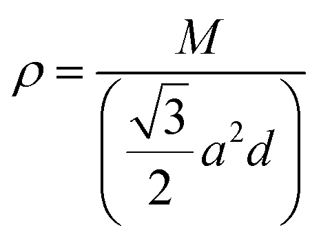 , with M being the mass of the MXene unit cell, a is the lattice parameter in the xy plane, and d denoting the MXene layer thickness.48 A bilayer Sc3(CN)F2 MXene structure model is optimized to calculate the layer thickness. The value of d = 10.284 Å is measured as the distance between two middle layer Sc atom planes in the bilayer Sc3(CN)F2 MXene. To accurately describe the interlayer interaction of the bilayers for Sc3(CN)F2, a zero damping van der Waals (vdW) correction (DFT-D3) of Grimme49 has been adopted. υj, ωmax,j and ωmin,j are the group velocity and the maximum and minimum circular frequency of each jth branch, respectively. Due to the finite flake length L, the term of ωmin,j is redefined as
 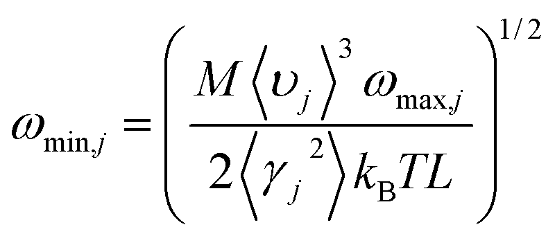 , where γj is the average value of the branch Grüneisen parameter, and 〈γ2j〉 in eqn (2) is estimated by
 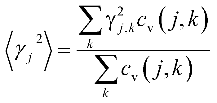 . Phonopy software50 combined with the VASP code is utilized for phonon dispersion calculations. The theoretical calculation is performed with density functional perturbation theory (DFPT),51 and a 6 × 6 × 1 k-points mesh based on a 2 × 2 × 1 super-cell is adopted for calculating the dynamical matrix. The thermal expansion coefficient α is investigated based on the Grüneisen approximation,52
  . Here, Nk is the k-point number adopted in plotting the phonon spectrum, which is equal to 120 in our calculations; Es is the strain energy; cv(j,k) is the (j,k) mode contribution to the heat capacity,
  . The Specific heat c is proportional to the heat capacity as
  .53
.53
The computational parameters and methods applied in calculating the carrier mobility and thermal properties have been tested in our previous works on Sc2CF2, Sc2C(OH)2 (ref. 54) and Hf2CO2 (ref. 55) MXenes. The predicted thermal conductivity of graphene in our previous calculation (4.76 × 10³ W m−1 K−1, based on a 5 μm flake length at room temperature) is consistent with the experimental results.56
Results and discussion
The geometries and band structure properties of the F terminated MXenes Sc3C2F2, Sc3N2F2 and Sc3(CN)F2 are investigated using DFT calculations. As 2D hexagonal materials, the MXenes possess two high-symmetry routes, namely, the y and x directions.57 The top view and side view of the Sc3(CN)F2 MXene are shown in Fig. 1(a) and (b). The Sc3C2F2 and Sc3N2F2 have similar structures to Sc3(CN)F2 and their side view diagrams are also shown in Fig. 2(a) and (b), respectively. According to our structure models, the x-axis coincides with the x direction, and the y-axis lies along the y direction. The Γ → K (Γ → X) and Γ → M (Γ → Y) vectors in the Brillouin zone correspond to the real-space x and y directions as shown in Fig. 1(c), respectively. The two carbon or nitrogen layers are sandwiched between three Sc layers, and two fluorine layers are projected onto the central Sc layer. Table 1 lists the lattice constants, formation energies and atomic layer distances marked in Fig. 2. The optimized lattice constant of Sc3(CN)F2 is similar to that of Sc3C2F2, and the formation energy is between that of Sc3C2F2 and Sc3N2F2. As with the result of the substituted C/N atoms, the Sc–F atomic layer distances are only slightly affected, while the Sc–C and Sc–N distances show notable variations, especially for the bonds with center Sc atoms (labelled as II in Table 1). The band structures of Sc3C2F2, Sc3N2F2 and Sc3(CN)F2 are also provided in Fig. 2 (vacuum energy is set as zero). Both Sc3C2F2 and Sc3N2F2 exhibit metallic properties with the Fermi level crossed by energy bands and with band gaps above/below the Fermi levels, while Sc3(CN)F2 is determined to be a semiconductor with an indirect band gap of 1.18 eV from HSE06. From the band structure plots, the three F terminated MXenes also exhibit similar shapes near the Fermi level despite the difference in band gaps. The band gap can also be observed from the partial density of states (PDOS) plot for Sc3(CN)F2 in Fig. 3. From the figure, Sc and N overlap from −4.5 to −2.5 eV, while Sc and C are from −2.5 to 0 eV (forming CBM) near the Fermi level. Sc3C2F2 and Sc3(CN)F2 show similar Fermi level energy; since the Sc–C bonds are strengthened in Sc3(CN)F2 as seen from the reduction of Sc–C bond lengths, the N atoms substitutions lowers the energy of Sc–C hybrid bands forming VBM bands in Sc3(CN)F2 relative to that in Sc3C2F2 around the Fermi level. Similarly, the CBM energy of Sc3(CN)F2 is raised relative to the corresponding bands in Sc3N2F2. These result in a rise of the band gap for Sc3(CN)F2 at a particular C/N ratio. This implies band engineering can be achieved in Sc-based MXenes by the structural design of the MXene, thus expanding the group of semiconducting MXenes. | ||
| Fig. 2 Band structures of three F terminated MXenes Sc3C2F2 (a), Sc3N2F2 (b) and Sc3(CN)F2 (c), and the vacuum energy is set as zero. Red solid and black dotted lines represent electronic energy bands from GGA-PBE and HSE06 respectively. The side view of the Sc3C2F2, Sc3N2F2 and Sc3(CN)F2 MXenes are shown below each band structure figure respectively. | ||
| MXene | a (Å) | Formation energy (eV per atom) (competing phase) | Atomic layer distance (Å) | |||||
|---|---|---|---|---|---|---|---|---|
| Sc–F | Sc–C | Sc–N | ||||||
| Sc3C2F2 | 3.243 | −1.77 (0.063; ScF3, Sc4C3, C) | 1.137 | 1.282(I) | 1.413(II) | — | — | |
| Sc3N2F2 | 3.190 | −2.70 (−0.057; ScF3, ScN, Sc) | 1.175 | — | — | 1.145(I) | 1.354(II) | |
| Sc3(CN)F2 | 3.244 | −2.29 (−0.052; ScF3, Sc4C3, ScN) | 1.133(I) | 1.155(II) | 1.273(I) | 1.264(II) | 1.066(I) | 1.524(II) |
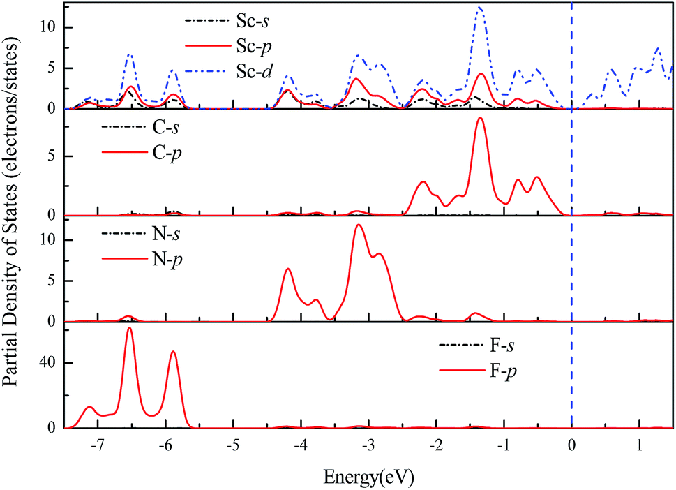 | ||
| Fig. 3 Partial density of states for the Sc3(CN)F2 MXene. | ||
With the semiconducting MXene Sc3(CN)F2 investigated in this work, its carrier mobilities with all the required parameters are then calculated and given in Table 2. From the table, the electron mobility of Sc3(CN)F2 by CBM, the red curve in Fig. 1(d), appears to be highly anisotropic, i.e. 1.348 × 103 cm2 V−1 s−1 along the x (Γ → X) and 0.319 × 103 cm2 V−1 s−1 along the y (Γ → Y) directions, respectively. For the hole mobilities, two quasi-degenerated sub-bands are present at the VBM as Fig. 1(d) indicates, and we distinguish the two sub-bands as “h1” (orange) and “h2” (blue), respectively. Both of the sub-bands have been calculated, and the total hole mobilities can be estimated as the statistical average of the two sub-bands on the basis of the Boltzmann distribution. Accordingly, the hole mobilities are determined to be 0.078 × 10³ along the x and along the y directions for the “h1” sub-band, and are 0.956 × 10³ along the x and 1.003 × 103 cm2 V−1 s−1 along the y directions for the “h2” sub-band, respectively. From Table 2, one may note that, for the “h1” or “h2” sub-band, the values of the effective mass and deformation potential constant along the x and y directions are close to each other, analogous to the Sc2CT2 MXenes calculated in our previous work.54 The average hole mobilities of Sc3(CN)F2 are 0.517 × 10³ along x and 0.540 × 103 cm2 V−1 s−1 along the y directions, respectively. Consequently, the predicted hole mobilities for Sc3(CN)F2 are almost isotropic. The details of the carrier effective mass calculations are provided in the ESI.† Actually, the electron mobilities are slightly lower than that of Sc2CF2 and Sc2C(OH)2, while the hole mobilities are higher than that of Sc2CF2 and Sc2C(OH)2.30 The predicted carrier mobilities are much higher than that of monolayer MoS2,58 providing a hopeful application in nanoelectronics devices for the Sc3(CN)F2 MXene. Moreover, in order to exclude the impact of structural disorder, i.e. the entropy effect on the semiconducting nature of Sc3(CN)F2, the possibilities of a random distribution of C and N atoms are taken into consideration as well. Three 2 × 2 × 1 super-cells with different C and N arrangement models are built for band structure calculations as shown in Fig. 4. Model 0 represents the ordered arrangement of C and N, and Model 1 and 2 are disordered ones. The results confirm that the Sc3(CN)F2 MXene is a semiconductor and imply that the random C and N distribution can lead to a slight sub band splitting of CBM and VBM, while the slopes of the bands near the Fermi level keep similar trends, suggesting that the ordered or disordered Sc3(CN)F2 MXene might have similar carrier mobilities.
 and
and  are the effective masses along the x and y directions. Ex and Ey are the deformation potential constants, Cx and Cy are the elastic moduli. μx and μy are the room-temperature carrier mobilities
| Carrier type |
|
|
Ex (eV) | Ey (eV) | Cx (J m−2) | Cy (J m−2) | μx (103 cm2 V−1 s−1) | μy (103 cm2 V−1 s−1) |
|---|---|---|---|---|---|---|---|---|
| e | 0.21 | 1.70 | 5.722 | 4.144 | 262.15 | 262.17 | 1.348 | 0.319 |
| h1 | 2.93 | 2.81 | 4.422 | 4.622 | 262.15 | 262.17 | 0.078 | 0.078 |
| h2 | 0.51 | 0.53 | −3.098 | −2.894 | 262.15 | 262.17 | 0.956 | 1.003 |


 | ||
| Fig. 4 (a) Band structures of Sc3(CN)F2 in Model 0, 1 and 2, the Fermi level located at zero; (b) the C (black) and N (blue) atoms arrangement models sketch, atoms under the gray semi-transparent interfaces present the second layer atoms. | ||
The Sc3C2F2, Sc3N2F2 and Sc3(CN)F2 MXenes phonon dispersions along Γ → M → K → Γ are given in Fig. 5. From the figure, the absence of imaginary phonon frequencies implies the structural stabilities of those MXenes. It is well known that thermal conductivities for semiconductive materials are dominantly contributed by phonon transport. Therefore, the lattice thermal conductivities for Sc3(CN)F2 are thus investigated in the current work and the electronic thermal conductivity for Sc3(CN)F2 is considered negligible. The values for the Sc3(CN)F2 MXene are calculated according to eqn (2) based on the phonon dispersions. The required parameters, including the group velocity υj, Grüneisen parameter γj and the square of the Grüneisen parameter 〈γ2j〉 are list in Table 3. From the table, the group velocities along the Γ → M (real-space y) direction for transversal acoustic (TA), longitudinal acoustic (LA) and out-of-plane acoustic (ZA) modes are larger than the Γ → K (real-space x) direction. In particular, the group velocity values for the ZA mode along Γ → M are approximately 20% higher. Moreover, the minimum values for Grüneisen parameter γj and 〈γ2j〉 found originated from the ZA mode along the Γ → M direction. For the Γ → K direction, the minimum in γj and 〈γ2j〉 occurs in the LA mode. The ratio of 〈γ2j〉 between the Γ → K and Γ → M directions is the maximum by the ZA mode. These may imply that the out of plane phonon modes are responsible for anisotropy in thermal conductance. Similar phenomena can be found in the parameters for calculating the thermal conductivities of Sc2CF2, Zr2CO2 and Hf2CO2 MXenes. Based on the parameters obtained, the thermal conductivities of Sc3(CN)F2 have been calculated.
 | ||
| Fig. 5 The phonon dispersions of the Sc3C2F2 (a), Sc3N2F2 (b) and Sc3(CN)F2 (c) MXenes. | ||
| υj (m s−1) | γj | 〈γj2〉 | |||||||
|---|---|---|---|---|---|---|---|---|---|
| TA | LA | ZA | TA | LA | ZA | TA | LA | ZA | |
| Γ → M | 3387 | 3897 | 3301 | 2.901 | 1.189 | 0.942 | 8.685 | 2.254 | 0.899 |
| Γ → K | 3220 | 3431 | 2758 | 1.909 | 1.574 | 1.893 | 4.263 | 2.591 | 4.032 |
The thermal conductivity is dependent upon the flake length d due to the existence of boundary scattering. The theoretical temperature dependence thermal conductivity of Sc3(CN)F2 with flake lengths of 5 μm along the Γ → M and Γ → K directions with TA, LA and ZA contributions are plotted in Fig. 6(a) and (b), respectively. The ZA mode has the highest contribution to the theoretical thermal conductivity along the Γ → M direction, due to the small value for the square of the Grüneisen parameter 〈γ2j〉, and the same is for the LA mode along the Γ → M direction. At room temperature (300 K), the calculated total thermal conductivities with TA, LA and ZA contributions along the Γ → M and Γ → K directions are 179 and 75.0 W m−1 K−1, respectively. The anisotropy in thermal conductivity is similar with that for other MXenes such as Sc2CF2, Sc2C(OH)2,54 Ti2CO2, Zr2CO2 and Hf2CO2,55 demonstrating that anisotropic thermal conductivity may be a common feature for semiconducting MXenes including Sc3(CN)F2. The temperature dependent thermal conductivities for the Sc3(CN)F2 MXene with flake lengths of 1–100 μm along the Γ → M and Γ → K directions are shown in Fig. 6(c) and (d), respectively. From the figure, the thermal conductivity increases monotonically with increasing flake length in both directions, and is more sensitive to the flake length at low temperatures. The room temperature thermal conductivity along the Γ → M direction increases from 123 to 283 W m−1 K−1 as the flake length increases from 1 to 100 μm, which can be understood as analogous to grain size controlled thermal conductivity for bulk materials. Comparatively, the thermal conductivity along the Γ → K direction increases from 55.7 to 111 W m−1 K−1, approximately half of that in the Γ → M direction. Despite that the room temperature thermal conductivity is much lower than the values in the range 4.84 (± 0.44) × 103 to 5.30 (± 0.48) × 103 W m−1 K−1 for single-layer graphene,56 the values for Sc3(CN)F2 and other MXenes like Sc2CT2 (T = F, OH) are of the same order of magnitude, higher than that of the phosphorene59 and monolayer MoS2.60 These results indicate that the Sc3(CN)F2 possesses good heat dissipation performance if used as an electronic device.
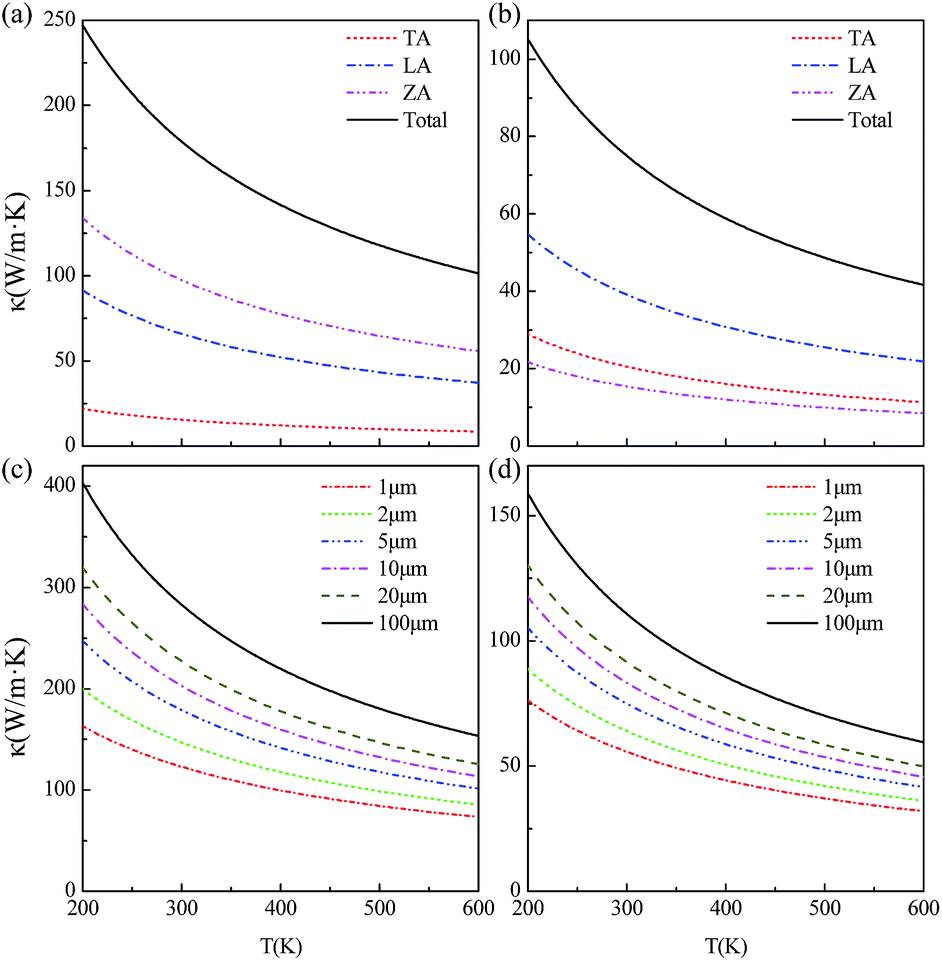 | ||
| Fig. 6 The temperature dependence thermal conductivities for the Sc3(CN)F2 MXene along the Γ → M (a) and Γ → K (b) directions with 5 μm flake length with TA, LA and ZA contributions. The temperature dependence thermal conductivities for the Sc3(CN)F2 MXene with 1–100 μm flake lengths along the Γ → M (c) and Γ → K (d) directions. | ||
The specific heat and thermal expansion coefficient are also studied from the phonon dispersion for the hexagonal BZ of Sc3(CN)F2, and the corresponding temperature dependence for Sc3(CN)F2 are shown in Fig. 7(a) and (b). These results suggest that both the specific heat and thermal expansion coefficient are positively related to the temperature, and the room temperature values are 547 J kg−1 K−1 and 8.703 × 10⁻⁶ K−1, respectively. By contrast, the specific heat and thermal expansion coefficient are 385 J kg−1 K−1 and 16.5 × 10⁻⁶ K−1 for copper, and 412 J kg−1 K−1 and 11.8 × 10⁻⁶ K−1 for iron. In addition, the room temperature specific heat is much higher than the value of 238 J kg−1 K−1 due to the relatively small relative atomic mass of Sc and the thermal expansion coefficient is close to the value of 6.094 × 10⁻⁶ K−1 for Hf2CO2 MXene.55 The relatively high specific heat and low thermal expansion coefficient make Sc3(CN)F2 a good candidate material for nanoelectronic devices.
 | ||
| Fig. 7 (a) The temperature dependence of Sc3(CN)F2 specific heat. (b) The temperature dependence of the Sc3(CN)F2 thermal expansion coefficient. | ||
Conclusions
In this work, we report our design and theoretical calculations of the semiconducting MXene Sc3(CN)F2. Different from the mother metallic Sc3C2F2 and Sc3N2F2 MXenes, the Sc3(CN)F2 MXene is a semiconductor with an indirect band gap of 1.18 eV from the HSE06 band structures analysis. The electrical and thermal properties of the Sc3(CN)F2 MXene are subsequently predicted by the current computational study. The Sc3(CN)F2 presents great anisotropy in electron mobility, and approximate isotropy in hole mobility. The electron mobilities of Sc3(CN)F2 are 1.348 × 10³ along x and 0.319 × 103 cm2 V−1 s−1 along the y directions, and the hole mobilities are 0.517 × 10³ along x and 0.540 × 103 cm2 V−1 s−1 along the y directions, respectively. The thermal conductivities for the Sc3(CN)F2 are studied with flake lengths of 1–100 μm. The thermal conductivity increases monotonically with increasing flake length, and the room temperature thermal conductivity along the Γ → M direction is 179 W m−1 K−1 with a flake length of 5 μm. In addition, the relatively high specific heat and low thermal expansion coefficient make Sc3(CN)F2 a good candidate material for nanoelectronic devices. The computational data provided here is expected to be meaningful for the expansion of the MXene family towards applications in electronic devices.Conflicts of interest
There are no conflicts to declare.Acknowledgements
The present work was supported by the National Key Research and Development Program of China (No. 2016YFB0700100), the Ningbo Municipal Key Project (2014S10001), the National Natural Science Foundation of China (Grant No. 91226202 and 91426304), the “Strategic Priority Research Program” of the Chinese Academy of Sciences (Grant No. XDA02040105 and XDA03010305), the Key Research Program of Frontier Sciences, CAS (Grant No. QYZDB-SSW-JSC037), One Thousand Youth Talents plan, ITaP at Purdue University and the Special Program for Applied Research on Super Computation of the NSFC-Guangdong Joint Fund (the second phase) (U1501501 to Juan Li and Aiguo Wu) for computing resources, the key technology of nuclear energy 2014 CAS Interdisciplinary Innovation Team, and the Major Project of the Ministry of Science and Technology of China (Grant No. 2015ZX06004-001).Notes and references
- M. Naguib, V. N. Mochalin, M. W. Barsoum and Y. Gogotsi, Adv. Mater., 2014, 26, 982 CrossRef.
- Q. Hu, D. Sun, Q. Wu, H. Wang, L. Wang, B. Liu, A. Zhou and J. He, J. Phys. Chem. A, 2013, 117, 14253–14260 CrossRef PubMed.
- V. M. Hong Ng, H. Huang, K. Zhou, P. S. Lee, W. Que, J. Z. Xu and L. B. Kong, J. Mater. Chem. A, 2017, 5, 3039–3068 RSC.
- M. Khazaei, A. Ranjbar, M. Arai, T. Sasaki and S. Yunoki, J. Mater. Chem. C, 2017, 5, 2488–2503 RSC.
- B. Anasori, M. R. Lukatskaya and Y. Gogotsi, Nat. Rev. Mater., 2017, 2, 16098 CrossRef.
- P. Eklund, M. Beckers, U. Jansson, H. Högberg and L. Hultman, Thin Solid Films, 2010, 518, 1851–1878 CrossRef.
- P. Eklund, J. Rosen and P. O. Å. Persson, J. Phys. D: Appl. Phys., 2017, 50, 113001 CrossRef.
- B. Anasori, M. Dahlqvist, J. Halim, E. J. Moon, J. Lu, B. C. Hosler, E. N. Caspi, S. J. May, L. Hultman, P. Eklund, J. Rosén and M. W. Barsoum, J. Appl. Phys., 2015, 118, 94304 CrossRef.
- J. Lei, X. Zhang and Z. Zhou, Front. Physiol., 2015, 10, 276–286 CrossRef.
- M. Naguib, M. Kurtoglu, V. Presser, J. Lu, J. Niu, M. Heon, L. Hultman, Y. Gogotsi and M. W. Barsoum, Adv. Mater., 2011, 23, 4248–4253 CrossRef PubMed.
- M. Naguib, O. Mashtalir, J. Carle, V. Presser, J. Lu, L. Hultman, Y. Gogotsi and M. W. Barsoum, ACS Nano, 2012, 6, 1322–1331 CrossRef PubMed.
- U. Yorulmaz, A. Özden, N. K. Perkgöz, F. Ay and C. Sevik, Nanotechnology, 2016, 27, 335702 CrossRef PubMed.
- F. Shahzad, M. Alhabeb, C. B. Hatter, B. Anasori, S. Man Hong, C. M. Koo and Y. Gogotsi, Science, 2016, 353, 1137–1140 CrossRef PubMed.
- B. Anasori, Y. Xie, M. Beidaghi, J. Lu, B. C. Hosler, L. Hultman, P. R. C. Kent, Y. Gogotsi and M. W. Barsoum, ACS Nano, 2015, 9, 9507–9516 CrossRef PubMed.
- C. Si, J. You, W. Shi, J. Zhou and Z. Sun, J. Mater. Chem. C, 2016, 4, 11524–11529 RSC.
- C. Xu, L. Wang, Z. Liu, L. Chen, J. Guo, N. Kang, X. Ma, H. Cheng and W. Ren, Nat. Mater., 2015, 14, 1135–1141 CrossRef PubMed.
- L. M. Azofra, N. Li, D. R. MacFarlane and C. Sun, Energy Environ. Sci., 2016, 9, 2545–2549 RSC.
- A. Morales-Garcia, A. Fernandez-Fernandez, F. Vines and F. Illas, J. Mater. Chem. A, 2018, 6, 3381–3385 RSC.
- H. Weng, A. Ranjbar, Y. Liang, Z. Song, M. Khazaei, S. Yunoki, M. Arai, Y. Kawazoe, Z. Fang and X. Dai, Phys. Rev. B: Condens. Matter Mater. Phys., 2015, 92, 75436 CrossRef.
- M. Khazaei, A. Ranjbar, M. Arai and S. Yunoki, Phys. Rev. B, 2016, 94, 125152 CrossRef.
- H. Fashandi, V. Ivády, P. Eklund, A. L. Spetz, M. I. Katsnelson and I. A. Abrikosov, Phys. Rev. B: Condens. Matter Mater. Phys., 2015, 92, 155142 CrossRef.
- M. Ashton, K. Mathew, R. G. Hennig and S. B. Sinnott, J. Phys. Chem. C, 2016, 120, 3550–3556 CrossRef.
- Q. Tang, Z. Zhou and P. Shen, J. Am. Chem. Soc., 2012, 134, 16909–16916 CrossRef PubMed.
- M. Khazaei, M. Arai, T. Sasaki, C. Chung, N. S. Venkataramanan, M. Estili, Y. Sakka and Y. Kawazoe, Adv. Funct. Mater., 2013, 23, 2185–2192 CrossRef.
- X. Zha, K. Luo, Q. Li, Q. Huang, J. He, X. Wen and S. Du, Europhys. Lett., 2015, 111, 26007 CrossRef.
- M. Khazaei, M. Arai, T. Sasaki, M. Estili and Y. Sakka, Phys. Chem. Chem. Phys., 2014, 16, 7841–7849 RSC.
- M. Khazaei, A. Ranjbar, M. Ghorbani-Asl, M. Arai, T. Sasaki, Y. Liang and S. Yunoki, Phys. Rev. B, 2016, 93, 205125 CrossRef.
- B. Anasori, C. Shi, E. J. Moon, Y. Xie, C. A. Voigt, P. R. C. Kent, S. J. May, S. J. L. Billinge, M. W. Barsoum and Y. Gogotsi, Nanoscale Horiz., 2016, 1, 227–234 RSC.
- L. Kaikai, J. Tifeng, X. Ruirui, Z. Guodong, Z. Jingxin, Z. Lexin and P. Qiuming, Sci. China Mater., 2018, 61, 728–736 CrossRef.
- K. Xiong, P. Wang, G. Yang, Z. Liu, H. Zhang, S. Jin and X. Xu, Sci. Rep., 2017, 7, 15095 CrossRef PubMed.
- S. Kumar and U. Schwingenschl Ogl, Phys. Rev. B, 2016, 94, 35405 CrossRef.
- J. Liu, X. Kan, B. Amin, L. Gan and Y. Zhao, Phys. Chem. Chem. Phys., 2017, 19, 32253–32261 RSC.
- S. Wang, Y. Du and W. Liao, Chin. Phys. B, 2017, 26, 17806 CrossRef.
- Y. Lee, Y. Hwang and Y. Chung, ACS Appl. Mater. Interfaces, 2015, 7, 7163–7169 CrossRef PubMed.
- E. Balcı, Ü. Ö. Akkuş and S. Berber, J. Mater. Chem. C, 2017, 5, 5956–5961 RSC.
- G. Kresse and D. Joubert, Phys. Rev. B: Condens. Matter Mater. Phys., 1999, 59, 1758–1775 CrossRef.
- J. P. Perdew, J. A. Chevary, S. H. Vosko, K. A. Jackson, M. R. Pederson, D. J. Singh and C. Fiolhais, Phys. Rev. B: Condens. Matter Mater. Phys., 1992, 46, 6671–6687 CrossRef.
- J. Hafner, J. Comput. Chem., 2008, 29, 2044–2078 CrossRef PubMed.
- M. Marsman, J. Paier, A. Stroppa and G. Kresse, J. Phys.: Condens. Matter, 2008, 20, 64201 CrossRef PubMed.
- Y. Wang, S. Wang, Y. Lu, J. Jiang and S. A. Yang, Nano Lett., 2016, 16, 4576–4582 CrossRef PubMed.
- J. Xi, M. Long, L. Tang, D. Wang and Z. Shuai, Nanoscale, 2012, 4, 4348–4369 RSC.
- M. Zhou, X. Chen, M. Li and A. Du, J. Mater. Chem. C, 2017, 5, 1247–1254 RSC.
- J. Bardeen and W. Shockley, Phys. Rev., 1950, 80, 72–80 CrossRef.
- S. Bruzzone and G. Fiori, Appl. Phys. Lett., 2011, 99, 222108 CrossRef.
- R. Fei and L. Yang, Nano Lett., 2014, 14, 2884–2889 CrossRef PubMed.
- P. G. Klemens and D. F. Pedraza, Carbon, 1994, 32, 735–741 CrossRef.
- P. G. Klemens, Int. J. Thermophys., 2001, 22, 265–275 CrossRef.
- T. Li, Phys. Rev. B: Condens. Matter Mater. Phys., 2012, 85, 235407 CrossRef.
- S. Grimme, J. Antony, S. Ehrlich and H. Krieg, J. Chem. Phys., 2010, 132, 154104 CrossRef PubMed.
- A. Togo, F. Oba and I. Tanaka, Phys. Rev. B: Condens. Matter Mater. Phys., 2008, 78, 134106 CrossRef.
- X. Gonze and C. Lee, Phys. Rev. B: Condens. Matter Mater. Phys., 1997, 55, 10355–10368 CrossRef.
- N. Mounet and N. Marzari, Phys. Rev. B: Condens. Matter Mater. Phys., 2005, 71, 205214 CrossRef.
- M. Upadhyay Kahaly and U. V. Waghmare, Appl. Phys. Lett., 2007, 91, 23112 CrossRef.
- X. Zha, J. Zhou, Y. Zhou, Q. Huang, J. He, J. S. Francisco, K. Luo and S. Du, Nanoscale, 2016, 8, 6110–6117 RSC.
- X. Zha, Q. Huang, J. He, H. He, J. Zhai, J. S. Francisco and S. Du, Sci. Rep., 2016, 6, 27971 CrossRef PubMed.
- A. A. Balandin, S. Ghosh, W. Bao, I. Calizo, D. Teweldebrhan, F. Miao and C. N. Lau, Nano Lett., 2008, 8, 902–907 CrossRef PubMed.
- M. Xu, T. Liang, M. Shi and H. Chen, Chem. Rev., 2013, 113, 3766–3798 CrossRef PubMed.
- Y. Cai, G. Zhang and Y. Zhang, J. Am. Chem. Soc., 2014, 136, 6269–6275 CrossRef PubMed.
- R. Fei, A. Faghaninia, R. Soklaski, J. Yan, C. Lo and L. Yang, Nano Lett., 2014, 14, 6393–6399 CrossRef PubMed.
- R. Yan, J. R. Simpson, S. Bertolazzi, J. Brivio, M. Watson, X. Wu, A. Kis, T. Luo, A. R. Hight Walker and H. G. Xing, ACS Nano, 2014, 8, 986–993 CrossRef PubMed.
Footnote |
| † Electronic supplementary information (ESI) available. See DOI: 10.1039/c8ra03424a |
| This journal is © The Royal Society of Chemistry 2018 |