
 Open Access Article
 This Open Access Article is licensed under a Creative Commons Attribution-Non Commercial 3.0 Unported Licence
Low-temperature, simple and efficient preparation of perovskite solar cells using Lewis bases urea and thiourea as additives: stimulating large grain growth and providing a PCE up to 18.8%†
Cheng-Ming Hsieha,
Yung-Sheng Liaob,
Yan-Ru Linb,
Chih-Ping Chen *b,
Cheng-Min Tsaia,
Eric Wei-Guang Diaua and
Shih-Ching Chuang*a
*b,
Cheng-Min Tsaia,
Eric Wei-Guang Diaua and
Shih-Ching Chuang*a
aDepartment of Applied Chemistry, National Chiao Tung University, Hsinchu, Taiwan. E-mail: jscchuang@faculty.nctu.edu.tw
bDepartment of Materials Engineering, Ming Chi University of Technology, New Taipei City, Taiwan. E-mail: cpchen@mail.mcut.edu.tw
First published on 29th May 2018
Abstract
We demonstrated that two Lewis bases – urea and thiourea – acted as efficient additives for CH3NH3(MA)PbI3−xClx and MAPbI3 perovskite solar cells (PSCs) and observed a significant increase in PCE for the MAPbI3 devices in the presence of 1% urea with a remarkable PCE of 18.8% using an extremely low annealing temperature (85 °C).
Introduction
Perovskite solar cells (PSCs) have become one of the most promising candidate technologies in next generation photovoltaics because of their high performance, solution processing techniques and potentially low cost.1–6 The quality of perovskites can be improved by solvent annealing, thermal treatment,7,8 or using additives9–11 to alter the morphology of the perovskites. In recent reports, the PCEs can reach a maximum of 22.7%.5,6 Theoretically speaking, it may produce a PCE of more than 30% with an improvement in fill factor (FF) and open circuit voltage (Voc).12–14 The incorporation of additive has been recognized as an efficient methodology to increase the performance of PSCs.15–18 Previous reports have demonstrated that incorporating diiodooctane (DIO), NH4Cl19,20 and alkylammonium iodides11,21 can increase the performance of PSC devices. Furthermore, the inserting of bulky cations can induce formation of 2D perovskites, which has been shown to improve the stability of PSCs.22 Recently, studies on additives further suggested the passivation of grain boundaries of perovskites for PCE enhancement;23–26 for instances, doping perovskites with pyridine,27 tri(n-octyl)phosphine oxide,28 polymers9 and fullerenes.29,30 The use of these additives with particular functional groups led to an expansion of the perovskite grains and significantly reduced the recombination of charges at the grain boundaries of the perovskites.31 Typically, these grain boundaries ended with functionalities of either halogens or alkyl-ammonium ions. Because thermal instability of these structures led to formation of the under-coordinated lead ion (Pb2+) and Pb–I antisite defects at grain boundaries, such a notion increased the number of trap states leading to charge accumulation and carrier recombination.32 Yang and co-workers first used urea and thiourea as additives for CH3NH3(MA)PbI3 derived normal (ITO/TiO2) PSCs, and demonstrated a PCE of 18.25% using an annealing temperature of 100 °C.10 Meng et al. used DMSO/urea to increase the PCE of normal devices up to 20.06% with the perovskites (FAPbI3)0.75(MAPbI3)0.17(MAPbBr3)0.08 and urea derived anti-solvent washing process.33 Considering the complexity of perovskite compositions and the myriad fabricating parameters involved in the previous process, we explored the urea and thiourea as simple precursor additives for inverted (MAPbI3−xClx and MAPbI3) PSCs. We adopted the ITO/NiOx or PEDOT:PSS/perovskite/PCBM/Ag structure and found the performance up to 18.8% with little hysteresis for urea-derived devices using a low annealing temperature, as low as 85 °C. In particular, the grain size of perovskite can be grown up to 935 nm—which was as twice large as those using conventional method and became a key factor on contributing to the high PCE.Results and discussion
We studied the effects for perovskites in the presence of urea and thiourea (Fig. 1a), and analyzed these perovskites thin films (w/ or w/o additives) using ultraviolet-visible spectroscopy (UV-vis), scanning electron microscopy (SEM) and grazing incidence wide angle X-ray diffraction (GIWAXS) measurements and varied the fabricated conditions—annealing temperatures and film compositions. These Lewis bases induced the intermolecular forces and were proven to be the passivation for trap states and led to efficient inter-grain carriers transporting.27,32 First, we fabricated the PSCs using the structure of ITO/PEDOT:PSS/MAPbI3−xClx/PCBM/Ag. We manipulated the concentration of urea and thiourea to the MAPbI3−xClx system at 0.5%, 1%, and 3% as additives to 30 wt% of MAPbI3−xClx precursor. We observed that the layers of MAPbI3−xClx could turn into a dark brown perovskite within 10 seconds from yellow colored precursors upon annealing at 90 °C with the addition of 0.5%, 1% and 3% of urea and thiourea, respectively. For normal films, the precursor didn't change from yellow to dark brown at 90 °C in 60 minutes until an extended annealing for 2.5 h.34 The urea- and thiourea-derived films changed to opaque appearance in 30 minutes, which indicated an over-crystallization of the perovskites.34 Therefore, we reduced the temperature to 80, 75 and 65 °C and fixed the additive concentration with 0.5% and 1%. We observed that the surface of the perovskite films still over-crystallized when 0.5% and 1% of urea was added at 80 °C and heated at 75 °C for 2.5 hours, respectively (Fig. S1 and S2†). The addition of 1% urea at 65 °C for 4.5 h resulted in as similar appearance of perovskites as a normal cell as shown in Fig. S1.† Compared with the normal MAPbI3−xClx, the film showed as yellow as colored precursor (Fig. S3)†. Similar phenomena were observed for thiourea-derived films (Fig. S2c to c-2†). The addition of 0.5% thiourea at 70 °C for 2.5 hours allowed the optimized formation of perovskites. It was noteworthy that the transformation of MAPbI3−xClx from precursor to under the annealing temperature below 75 °C for 2 hours was incomplete for the perovskite films (w/o thiourea) since we can clearly observe the yellow appearance throughout the process. Fig. 1b showed the UV-vis for 1% urea (65 °C, 4.5 h) and 0.5% thiourea (75 °C, 2.5 h) derived films. Compared with normal films, we observed an increase in the intensity of the absorbance. This implied that the additives might improve the morphology (coverage) of MAPbI3−xClx.35 Similar phenomena was observed for MAPbI3 films when compared with the normal films at same fabrication condition with annealing at 100 °C for 10 min on NiOx surface (Fig. 1b).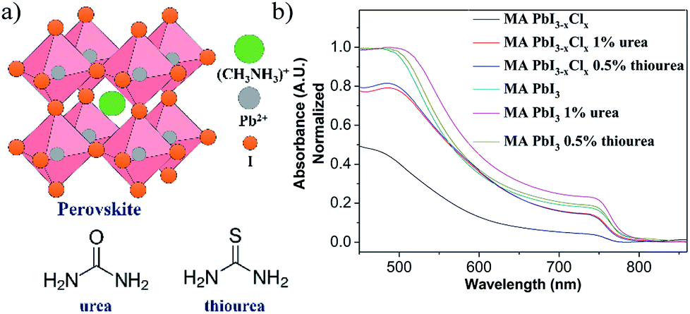 | ||
| Fig. 1 (a) Chemical structure of perovskite, urea and thiourea (b) UV-vis absorption spectra of perovskites with and without additives. | ||
For a standard MAPbI3−xClx, it required an annealing at 90 °C for 2.5 hours to provide a coverage rate of 94% (Fig. S4b†). The surface morphology of the MAPbI3−xClx (w/o additive at 65 °C for 4.5 h) exhibited more holes and with a coverage of 82.7% (Fig. S4a†). The incomplete transformation led to small grain size and poor surface coverage. As our expected, the surface coverage (97.7%) of the 1% urea-derived film (with a relatively lower annealing temperature of 65 °C for 4.5 hours) was greatly improved since the pores were reduced and the grain boundaries were relatively more continuous (Fig. S4c†). Compared with the devices annealed at 90 °C w/o additives, the coverage increased from 94.0% to 97.7% (Fig. S4b and c†). We found that the coverage of 0.5% thiourea derived perovskite showed a best coverage of 98.9% with the annealing temperature of 75 °C for 2.5 hours (Fig. S4d†). As shown in Fig. 2a–c, it can be observed that MAPbI3-based perovskites showed a significant increase in crystal grain size compared to normal perovskite thin film after addition of 1% urea with 100 °C annealing for 10 minutes—the grain size increased from 184.9 nm to 368.9 nm. Similarly, the grain size increased to 369.8 nm upon addition of 0.5% thiourea. We observed a significantly increase in grain size under 85 °C (10 min) annealing process. The grain sizes of 1% urea and 0.5% thiourea derived films increased from 102.0 nm to 935.1 and 891.0 nm, respectively (Fig. 2d–f). For 1% urea derived perovskites at an annealing temperature of 65 °C for 20 min, the grain size increased from 93.2 nm to 608.9 nm, and the grains by addition of 0.5% thiourea increased to 895.2 nm (Fig. S5a–c†). Therefore, it was evidenced by SEM analysis that the addition of small amount of urea or thiourea can efficiently promote the growth of MAPbI3−xClx thin films at a lower annealing temperature—resulting in a relatively flat film with less holes. In the MAPbI3, we observed the greatly increase in grain size of perovskites, implied electrons and holes can be more effectively transported to the corresponding charge transport layer, and lower leakage current was expected at the interfaces that enhanced the PCE.
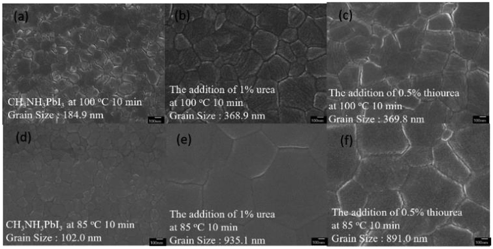 | ||
| Fig. 2 FE-SEM images of MAPbI3 perovskite thin films under different conditions (a) MAPbI3, (b) 1% urea, (c) 0.5% thiourea at 100 °C for 10 min, respectively; (d) MAPbI3, (e) 1% urea, (f) 0.5% thiourea at 85 °C for 10 min, respectively, (scale bar 100 nm). | ||
According to GIWAXS analysis in Fig. S6,† there were some (110) signatures but no significant (220) signatures when the MAPbI3−xClx based precursor was annealed at 65 °C for 4.5 hours without the addition of additives. We speculated that the annealing temperature could be too low to fully convert the precursor solution into perovskite thin film. With the increase of annealing temperature, it showed obvious characteristic peaks at (110) and (220) at 75 °C. It can be assumed that the precursor solution has been converted to a better perovskite thin film. However, upon addition of 1% urea with annealing at 65 °C, the significant (110) and (220) signature signals were observed. Therefore, it can be inferred that the precursor solution has been effectively converted into a perovskite thin film. However, after using 0.5% thiourea as an additive with annealing at 75 °C for 2.5 hours, intense (110) and (220) signature peaks of the perovskite thin film than the undoped perovskite were observed. It can be concluded that the precursor solution can be more effectively converted into a crystalline perovskite thin film using 0.5% thiourea as an additive. Therefore, it was proved that the annealing temperature can be reduced to help effectively conversion of the additives derived perovskite precursors into a well crystalline perovskite thin film by GIWAXS analysis. Furthermore, the intensity of the characteristic peaks, (110) and (220), changed—which proved that doping urea and thiourea as additives can effectively affect the nucleation and growth of the grains. Similar phenomenon was observed for MAPbI3, the addition of urea and thiourea in MAPbI3-based perovskites at 100 °C for 10 minutes showed an obvious and stronger characteristic peaks of (110) and (220) when compared with the MAPbI3 without additive (Fig. 3a). In an annealing temperature at 85 °C for 10 minutes, 1% urea derived MAPbI3 film showed stronger (110) and (220) characteristic peak signals and no other extra peaks were generated. This implied that the addition of urea in the MAPbI3 system can effectively help the grain growth and improve the efficiency in a relatively low temperature environment without affecting the perovskite structure.
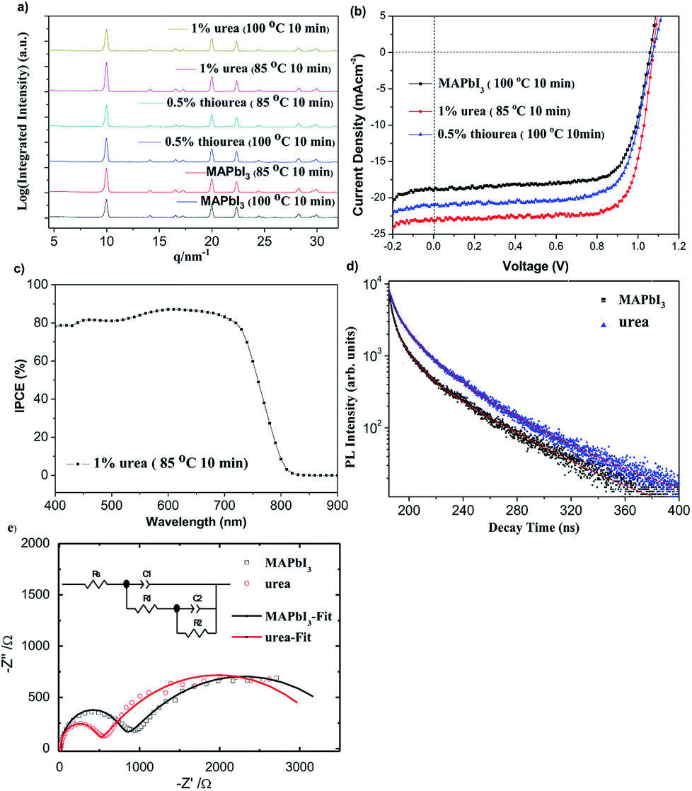 | ||
| Fig. 3 (a) GIWAXS patterns, (b) J–V curves, (c) IPCE, (d) TRPL decay curves and (e) electrochemical impedance spectral (EIS) Nyquist plots (the symbols are experimental data, the solid curves are fitting data and the corresponding electronic circuit is shown on top inset) for MAPbI3 PSCs. | ||
Table S1† summarized the performance of MAPbI3−xClx devices. The PCEs of normal devices (90 °C) were 8.8 ± 0.9%. According to Table S1 and Fig. S7,† upon addition of 1% urea and 0.5% thiourea to the perovskite devices, there were clear improvements on short circuit current density (Jsc) and Voc. We observed that the better perovskite thin films can be obtained at lower temperature upon addition of 1% urea or 0.5% thiourea as compared to the normal devices. The PCEs of the control devices at 65 °C was 4.1 ± 1.0% while the PCEs of 1% urea derived devices at the annealing temperature of 65 °C was 13.0 ± 0.39%. When compared with a normal cell, we observed an increase in PCEs of 34.7% from 9.8 to 13.2%. It was reproducible for the devices with addition of urea at the annealing temperature of 65 °C, so were the devices with doping 0.5% thiourea. Based on the Rsh values, we inferred that the Rsh values increased from 231.6 to 576.7 Ω cm2 upon doping with 1% urea. The resulted suggested that the perovskite precursor can be converted into a smooth MAPbI3−xClx with high coverage led to efficient hole/electron transport, low leakage current and improved in Jsc values; therefore, the PCE of the PSC device was relatively increased. The device showed a slight increase in Jsc upon addition of 0.5% thiourea as an additive, presumably because of the good surface morphology of the perovskite thin film after annealing. Therefore, it caused reduction of energy levels and defects; a larger parallel resistance was resulted. As shown in Table 1, the PCEs of normal MAPbI3-based devices prepared at 100 °C were 14.4 ± 0.3%. With the addition of 1% urea and 0.5% thiourea, the Jsc and FF values were significantly increased at different heating temperatures, so that the PCEs can be increased. The PCEs of the normal devices at 85 °C was 13.1 ± 0.3% (Table S2†). The PCEs of the 1% urea derived devices (85 °C) was 18.5 ± 0.3 with a best performance of 18.8%, along with a Jsc of 22.58 mA cm−2, the Voc of 1.06 V and the FF of 78.5% (Table 1 and Fig. 3b). The devices from 85 °C outperformed than those derived from the 100 °C process due to the greater grain size (Fig. 2). At an annealed temperature of 65 °C (10 min), the PCEs of the normal devices were 7.0 ± 0.2% while the PCEs of the 1% urea derived devices were 15.9 ± 0.3%. This value is record high among the highest reported performance for PSC under such low annealing condition. We observed an increase in performance for the devices in the presence of 0.5% thiourea (at the annealing temperature of 100 °C) with the PCEs 16.2 ± 0.05% (Table S2 and Fig. S8†). Since hysteresis effect appeared to be widespread in PSCs, we found that the hysteresis effect of the device after addition of 1% urea (85 °C, 10 min) was not significant, and the J–V curves for the forward and reverse scans with various delay times were similar (Table S3†).
| Devices | Condition | Jsc (mA cm−2) | Voc (V) | FF (%) | PCE (%) | PCEa (%) |
|---|---|---|---|---|---|---|
| a Best performance.b Rsh = 1417.1 Ω cm2, Rs = 32.8 Ω cm2.c Rsh = 3003.3 Ω cm2, Rs = 31.3 Ω cm2.d Rsh = 1030.2 Ω cm2, Rs = 30.2 Ω cm2. | ||||||
| Normal | 100 °C (10 min) | 19.0 ± 0.4 | 1.05 ± 0.02 | 73.8 ± 2.2 | 14.4 ± 0.3 | 14.6b |
| Urea | 85 °C (10 min) | 22.4 ± 0.2 | 1.06 ± 0.01 | 77.9 ± 1.2 | 18.5 ± 0.3 | 18.8c |
| Thiourea | 100 °C (10 min) | 21.0 ± 0.0 | 1.07 ± 0.01 | 72.2 ± 0.1 | 16.2 ± 0.1 | 16.2d |
Based upon the incident photon-to-current efficiency (IPCE) graph in Fig. S9,† the spectra of MAPbI3−xClx PSCs were similar. The contribution of IPCE was about located at wavelengths of 400 and 800 nm. At annealing temperature of 65 °C for 4.5 hours, the maximum of IPCE located at 600 nm increased from 17% to 77% after using 1% urea as additives. It was presumed that the perovskites with additives were effectively modified so that defects and trap levels were reduced. Therefore, it required less energy for grain growth and achieved a comparably high Jsc value at 65 °C. It can be observed from Fig. S10† that the main contribution of IPCE spectra was about 450 nm to 750 nm upon addition of 0.5% thiourea under the same annealing conditions, in which IPCE increased from 73.9% to 83.9% (640 nm). Because the increase in grain size and UV-vis absorbance, the 1% urea derived MAPbI3 devices showed the highest IPCE located at 610 nm with an intensity of 87.4% (Fig. 3c and S10†). To further investigate the effects on performance of MAPbI3-based perovskite thin films upon adding urea, we conducted a time-resolved photoluminescence (TRPL) measurements. Fig. 3d showed PL decay curves of MAPbI3-based perovskite thin films and the addition of 1% urea perovskite thin films. Table. S4† summarized the PL carrier lifetimes parameters. We found that lifetimes τ1 (ns) and τ2 (ns) were only 10.3 ns and 2.3 ns, respectively, when MAPbI3-based perovskites were urea free. After urea was added, τ1 (ns) and τ2 (ns) increased to 16.1 ns and 4.3 ns, respectively. This indicated that the addition of urea can prolong the carrier life-time and reduce the occurrence of trap defects and recombination. To characterize the internal resistance and charge transfer kinetics of PSCs w/ or w/o additive, electrochemical impedance spectroscopy (EIS) was performed under illumination with same light intensity as AM1.5G. The Nyquist plots and fitting curves are illustrated in Fig. 3e, showing two semicircles in the frequency range 100 mHz to 4 MHz. The experimental data were fitted quite well according to the equivalent circuit model shown in the inset of the figure; the fitting parameters are summarized in Table S5†. For the fitting results, the RS represents the series resistance of the ITO substrate. The semicircles in the high frequency region are related to C1 and R1, representing the charge transfer in the perovskite layer; C1 might be dominated by the geometric capacitance and may contain components of contact layers responding in a high-frequency domain.36 The semicircle represented by C2 and R2 in the low frequency region reflects the interfacial charge recombination processes. The Nyquist plots show the urea-derived device with a lower charge-transfer resistance (R1) than that normal device, indicating that the charge transfer inside the perovskite layers were more efficient for the former than latter (the normal cell). The R2 of both devices showed similar charge-recombination (RC) resistance, indicating that the CR rates in the perovskite/HTL or perovskite/ETL interface were similar and this explains both devices have similar open-circuit voltages. These results imply that urea in perovskite could improve the charge transfer of the perovskite layer, thus enhancing the corresponding device performance compared to the reference cell without an additive. Fig. S11† displayed the PL spectra of the normal and urea derived perovskite films on glass without NiOx. Because of larger crystal size for urea–perovskite, we observed an improvement in the PL intensity. The phenomenon is consistence with TRPL result.
Conclusions
We have demonstrated a lower temperature perovskites formation process through addition of 1% urea and 0.5% thiourea into the precursor of MAPbI3−xClx or MAPbI3 perovskite. We found that urea can effectively convert the perovskites precursor solution into a better surface, grain size and crystalline perovskite thin film at a relatively low temperature. Through this technique, we improved the PCE of the MAPbI3−xClx devices from 4.1 ± 1.0% to 13.0 ± 0.4% with a higher surface coverage from 82.7% to 97.7%. The addition of urea and thiourea as additives to MAPbI3-based PCSs has similar effects. We found that PCEs can be increased by up to 18.8% (18.5 ± 0.3) from the 13.1 ± 0.3% at an annealing temperature of 85 °C for 10 minutes upon adding 1% urea. PCEs can be increased by up to 16.2% (15.9 ± 0.3%) from the 7.0 ± 0.2% upon annealing at 65 °C for 20 minutes after the addition of 1% urea. The addition of urea and thiourea can promote grain growth and reduce the grain boundary of the thin film in MAPbI3-based devices, allowing the electron and hole to be transferred more effectively. As a result, this additive technique provided modification of defects and traps of perovskites that has improved overall efficiency and reproducibility.Experimental
All chemicals were purchased from Aldrich and used as received, unless otherwise specified. MAI was synthesized according to previously reported techniques.37 The detailed experimental and fabricated conditions are shown in the ESI.†Conflicts of interest
There are no conflicts to delcare.Acknowledgements
We thank the Ministry of Science and Technology of Taiwan (MOST 106-2113-M-131-001-MY2 and MOST 104-2113-M-009-014-MY3) for financial support.Notes and references
- P.-L. Qin, Q. He, C. Chen, X.-L. Zheng, G. Yang, H. Tao, L.-B. Xiong, L. Xiong, G. Li and G.-J. Fang, High-Performance Rigid and Flexible Perovskite Solar Cells with Low-Temperature Solution-Processable Binary Metal Oxide Hole-Transporting Materials, Sol. RRL, 2017, 1(8), 1700058 CrossRef.
- P. L. Qin, G. Yang, Z. W. Ren, S. H. Cheung, S. K. So, L. Chen, J. Hao, J. Hou and G. Li, Stable and Efficient Organo-Metal Halide Hybrid Perovskite Solar Cells via pi-Conjugated Lewis Base Polymer Induced Trap Passivation and Charge Extraction, Adv. Mater., 2018, 30(12), e1706126 CrossRef PubMed.
- H. L. Zhu, Z. Liang, Z. Huo, W. K. Ng, J. Mao, K. S. Wong, W.-J. Yin and W. C. H. Choy, Low-Bandgap Methylammonium-Rubidium Cation Sn-Rich Perovskites for Efficient Ultraviolet-Visible-Near Infrared Photodetectors, Adv. Funct. Mater., 2018, 0(0), 1706068 CrossRef.
- Z. Zhu, D. Zhao, C.-C. Chueh, X. Shi, Z. Li and A. K. Y. Jen, Highly Efficient and Stable Perovskite Solar Cells Enabled by All-Crosslinked Charge-Transporting Layers, Joule, 2018, 2(1), 168–183 CrossRef.
- J.-P. Correa-Baena, M. Saliba, T. Buonassisi, M. Grätzel, A. Abate, W. Tress and A. Hagfeldt, Promises and challenges of perovskite solar cells, Science, 2017, 358(6364), 739–744 CrossRef PubMed.
- J. Huang, Y. Yuan, Y. Shao and Y. Yan, Understanding the physical properties of hybrid perovskites for photovoltaic applications, Nat. Rev. Mater., 2017, 2, 17042 CrossRef.
- T. Li, Y. Pan, Z. Wang, Y. Xia, Y. Chen and W. Huang, Additive engineering for highly efficient organic-inorganic halide perovskite solar cells: recent advances and perspectives, J. Mater. Chem. A, 2017, 5(25), 12602–12652 Search PubMed.
- D. Ouyang, J. Xiao, F. Ye, Z. Huang, H. Zhang, L. Zhu, J. Cheng and W. C. H. Choy, Strategic Synthesis of Ultrasmall NiCo2O4 NPs as Hole Transport Layer for Highly Efficient Perovskite Solar Cells, Adv. Energy Mater., 2018, 0(0), 1702722 CrossRef.
- L. Zuo, H. Guo, D. W. deQuilettes, S. Jariwala, N. De Marco, S. Dong, R. DeBlock, D. S. Ginger, B. Dunn, M. Wang and Y. Yang, Polymer-modified halide perovskite films for efficient and stable planar heterojunction solar cells, Sci. Adv., 2017, 3(8), e1700106 CrossRef PubMed.
- J.-W. Lee, S.-H. Bae, Y.-T. Hsieh, N. De Marco, M. Wang, P. Sun and Y. Yang, A Bifunctional Lewis Base Additive for Microscopic Homogeneity in Perovskite Solar Cells, Chem, 2017, 3(2), 290–302 Search PubMed.
- H. L. Hsu, C. C. Chang, C. P. Chen, B. H. Jiang, R. J. Jeng and C. H. Cheng, High-performance and high-durability perovskite photovoltaic devices prepared using ethylammonium iodide as an additive, J. Mater. Chem. A, 2015, 3(17), 9271–9277 Search PubMed.
- N. Li, Z. Zhu, Q. Dong, J. Li, Z. Yang, C. C. Chueh, A. K. Y. Jen and L. Wang, Enhanced Moisture Stability of Cesium-Containing Compositional Perovskites by a Feasible Interfacial Engineering, Adv. Mater. Interfaces, 2017, 4(20), 1700598 CrossRef.
- E. Ercan, J. Y. Chen, P. C. Tsai, J. Y. Lam, S. C. W. Huang, C. C. Chueh and W. C. Chen, A Redox-Based Resistive Switching Memory Device Consisting of Organic–Inorganic Hybrid Perovskite/Polymer Composite Thin Film, Adv. Electron. Mater., 2017, 3(12), 1700344 CrossRef.
- M. Abdi-Jalebi, Z. Andaji-Garmaroudi, S. Cacovich, C. Stavrakas, B. Philippe, J. M. Richter, M. Alsari, E. P. Booker, E. M. Hutter, A. J. Pearson, S. Lilliu, T. J. Savenije, H. Rensmo, G. Divitini, C. Ducati, R. H. Friend and S. D. Stranks, Maximizing and stabilizing luminescence from halide perovskites with potassium passivation, Nature, 2018, 555, 497 CrossRef PubMed.
- G. Xiu, L. Meng, S. Xiao-Bo, M. Heng, W. Zhao-Kui and L. Liang-Sheng, Controllable Perovskite Crystallization by Water Additive for High-Performance Solar Cells, Adv. Funct. Mater., 2015, 25(42), 6671–6678 CrossRef.
- J. Lu-Lu, W. Zhao-Kui, L. Meng, Z. Cong-Cong, Y. Qing-Qing, H. Ke-Hao, L. Ding-Ze, F. Peng-Fei and L. Liang-Sheng, Passivated Perovskite Crystallization via g-C3N4 for High-Performance Solar Cells, Adv. Funct. Mater., 2018, 28(7), 1705875 CrossRef.
- C.-C. Zhang, M. Li, Z.-K. Wang, Y.-R. Jiang, H.-R. Liu, Y.-G. Yang, X.-Y. Gao and H. Ma, Passivated perovskite crystallization and stability in organic-inorganic halide solar cells by doping a donor polymer, J. Mater. Chem. A, 2017, 5(6), 2572–2579 Search PubMed.
- M. Li, Y.-H. Chao, T. Kang, Z.-K. Wang, Y.-G. Yang, S.-L. Feng, Y. Hu, X.-Y. Gao, L.-S. Liao and C.-S. Hsu, Enhanced crystallization and stability of perovskites by a cross-linkable fullerene for high-performance solar cells, J. Mater. Chem. A, 2016, 4(39), 15088–15094 Search PubMed.
- P. W. Liang, C. Y. Liao, C. C. Chueh, F. Zuo, S. T. Williams, X. K. Xin, J. Lin and A. K. Jen, Additive enhanced crystallization of solution-processed perovskite for highly efficient planar-heterojunction solar cells, Adv. Mater., 2014, 26(22), 3748–3754 CrossRef PubMed.
- C. Zuo and L. Ding, An 80.11% FF record achieved for perovskite solar cells by using the NH4Cl additive, Nanoscale, 2014, 6(17), 9935–9938 RSC.
- C.-M. Hsieh, Y.-L. Yu, C.-P. Chen and S.-C. Chuang, Effects of the additives n-propylammonium or n-butylammonium iodide on the performance of perovskite solar cells, RSC Adv., 2017, 7(88), 55986–55992 RSC.
- Y. Chen, Y. Sun, J. Peng, W. Zhang, X. Su, K. Zheng, T. Pullerits and Z. Liang, Tailoring Organic Cation of 2D Air-Stable Organometal Halide Perovskites for Highly Efficient Planar Solar Cells, Adv. Energy Mater., 2017, 7(18), 1700162 CrossRef.
- Z. Huang, X. Duan, Y. Zhang, X. Hu, L. Tan and Y. Chen, Pure- or mixed-solvent assisted treatment for crystallization dynamics of planar lead halide perovskite solar cells, Sol. Energy Mater. Sol. Cells, 2016, 155(suppl. C), 166–175 CrossRef.
- A. R. Pascoe, S. Meyer, W. Huang, W. Li, I. Benesperi, N. W. Duffy, L. Spiccia, U. Bach and Y.-B. Cheng, Enhancing the Optoelectronic Performance of Perovskite Solar Cells via a Textured CH3NH3PbI3 Morphology, Adv. Funct. Mater., 2016, 26(8), 1278–1285 CrossRef.
- Y. Zhang, L. Tan, Q. Fu, L. Chen, T. Ji, X. Hu and Y. Chen, Enhancing the grain size of organic halide perovskites by sulfonate-carbon nanotube incorporation in high performance perovskite solar cells, Chem. Commun., 2016, 52(33), 5674–5677 RSC.
- L. Zheng, D. Zhang, Y. Ma, Z. Lu, Z. Chen, S. Wang, L. Xiao and Q. Gong, Morphology control of the perovskite films for efficient solar cells, Dalton Trans., 2015, 44(23), 10582–10593 RSC.
- N. K. Noel, A. Abate, S. D. Stranks, E. S. Parrott, V. M. Burlakov, A. Goriely and H. J. Snaith, Enhanced Photoluminescence and Solar Cell Performance via Lewis Base Passivation of Organic–Inorganic Lead Halide Perovskites, ACS Nano, 2014, 8(10), 9815–9821 CrossRef PubMed.
- D. W. deQuilettes, S. Koch, S. Burke, R. K. Paranji, A. J. Shropshire, M. E. Ziffer and D. S. Ginger, Photoluminescence Lifetimes Exceeding 8 μs and Quantum Yields Exceeding 30% in Hybrid Perovskite Thin Films by Ligand Passivation, ACS Energy Lett., 2016, 1(2), 438–444 CrossRef.
- Y. H. Shao, Z. G. Xiao, C. Bi, Y. B. Yuan and J. S. Huang, Origin and elimination of photocurrent hysteresis by fullerene passivation in CH3NH3PbI3 planar heterojunction solar cells, Nat. Commun., 2014, 5, 5784 CrossRef PubMed.
- J. Xu, A. Buin, A. H. Ip, W. Li, O. Voznyy, R. Comin, M. Yuan, S. Jeon, Z. Ning, J. J. McDowell, P. Kanjanaboos, J.-P. Sun, X. Lan, L. N. Quan, D. H. Kim, I. G. Hill, P. Maksymovych and E. H. Sargent, Perovskite–fullerene hybrid materials suppress hysteresis in planar diodes, Nat. Commun., 2015, 6, 7081 CrossRef PubMed.
- D.-Y. Son, J.-W. Lee, Y. J. Choi, I.-H. Jang, S. Lee, P. J. Yoo, H. Shin, N. Ahn, M. Choi, D. Kim and N.-G. Park, Self-formed grain boundary healing layer for highly efficient CH3 NH3 PbI3 perovskite solar cells, Nat. Energy, 2016, 1, 16081 CrossRef.
- T. Niu, J. Lu, R. Munir, J. Li, D. Barrit, X. Zhang, H. Hu, Z. Yang, A. Amassian, K. Zhao and S. F. Liu, Stable High-Performance Perovskite Solar Cells via Grain Boundary Passivation, Adv. Mater., 2018, 0(0), 1706576 CrossRef PubMed.
- L. Zhu, Y. Xu, P. Zhang, J. Shi, Y. Zhao, H. Zhang, J. Wu, Y. Luo, D. Li and Q. Meng, Investigation on the role of Lewis bases in the ripening process of perovskite films for highly efficient perovskite solar cells, J. Mater. Chem. A, 2017, 5(39), 20874–20881 Search PubMed.
- H.-L. Hsu, C.-P. Chen, J.-Y. Chang, Y.-Y. Yu and Y.-K. Shen, Two-step thermal annealing improves the morphology of spin-coated films for highly efficient perovskite hybrid photovoltaics, Nanoscale, 2014, 6(17), 10281 RSC.
- J. Joseph and E. D. Jemmis, Red-, Blue-, or No-Shift in Hydrogen Bonds: A Unified Explanation, J. Am. Chem. Soc., 2007, 129(15), 4620–4632 CrossRef PubMed.
- F. Behrouznejad, C.-M. Tsai, S. Narra, E. W. G. Diau and N. Taghavinia, Interfacial Investigation on Printable Carbon-Based Mesoscopic Perovskite Solar Cells with NiOx/C Back Electrode, ACS Appl. Mater. Interfaces, 2017, 9(30), 25204–25215 Search PubMed.
- H.-L. Hsu, C.-C. Chang, C.-P. Chen, B.-H. Jiang, R.-J. Jeng and C.-H. Cheng, High-performance and high-durability perovskite photovoltaic devices prepared using ethylammonium iodide as an additive, J. Mater. Chem. A, 2015, 3(17), 9271–9277 Search PubMed.
Footnote |
| † Electronic supplementary information (ESI) available: Device fabrication condition and experimental detail. See DOI: 10.1039/c8ra03175d |
| This journal is © The Royal Society of Chemistry 2018 |