
 Open Access Article
 This Open Access Article is licensed under a Creative Commons Attribution-Non Commercial 3.0 Unported Licence
A III-nitride nanowire solar cell fabricated using a hybrid coaxial and uniaxial InGaN/GaN multi quantum well nanostructure
Ji-Hyeon Park,
R. Nandi,
Jae-Kwan Sim,
Dae-Young Um,
San Kang,
Jin-Soo Kim and
Cheul-Ro Lee *
*
Semiconductor Materials Process Laboratory, School of Advanced Materials Engineering, Engineering College, Research Center for Advanced Materials Development (RCAMD), Chonbuk National University, Baekje-daero 567, Jeonju 54896, Republic of Korea. E-mail: crlee7@jbnu.ac.kr
First published on 5th June 2018
Abstract
III-Nitride nanowires are currently considered as next generation photovoltaic materials due to their excellent physical properties together with reduced dislocation densities, increased surface area and thus enhanced light absorption and direct path for carrier transport. Here, we investigate the photovoltaic characteristics of a solar cell fabricated from a novel hybrid nanostructure comprising uniaxial and coaxial InGaN/GaN multi-quantum wells (MQWs) along with an InGaN nano-cap layer. Various characterization methods were employed to study the optical and structural properties of the hybrid nanostructure. Transmission electron microscopy images revealed the hybrid nanostructure consists of distinct uniaxial and coaxial InGaN/GaN MQWs along with the InGaN nano-cap layer. The InGaN/GaN MQW architectures have a significant effect on the performance of the photovoltaic device. The solar cell fabricated with the hybrid nanostructure exhibits superior photovoltaic performance compared to the uniaxial as well as the coaxial InGaN/GaN nanowire MQW structures. The improved photovoltaic characteristic is primarily attributed to the considerably larger InGaN active area grown in the hybrid nanostructure. A conversion efficiency of 1.16% along with a fill factor of 70% was obtained for the device fabricated with the hybrid nanostructure. This study provides an experimental demonstration of the improvement of III-nitride nanowire based solar cells incorporating uniaxial and coaxial InGaN/GaN MQWs.
1. Introduction
Considering the importance of the worldwide energy demand, the use of photovoltaic devices is widely attractive as an abundant, clean and renewable energy approach. III-Nitride semiconductors are presently under study as a potential alternative to conventional photovoltaic absorber materials for the realization of high efficiency solar cells.1–9 In particular, the entire solar spectrum can be absorbed by the InxGa1−xN system through tuning its direct band gap by optimizing the In composition.10 Moreover, excellent physical properties, such as high mobility, drift velocity, radiation, thermal conductivity and high temperature resistance leading to long lifetime and strong optical absorption, which render InGaN alloys a possible substitute for the conventional solar cell absorbers.10–12 Additionally, InGaN-based solar cells have the potential to operate under harsh environments, where Si solar cells may suffer from unstable operation.8 Likewise, in 2007, Zhang et al. calculated the conversion efficiency of III-nitride photovoltaics in details. They reported an efficiency upto ∼20% from single In0.65Ga0.35N cell.13 In another report, they have also shown that the efficiency can be increased to 35.1% using InGaN/GaN two-junction cells.14 In the same context, Hsu et al. calculated the efficiency of InGaN/Si tandem solar cells can be increased to 35% using double InGaN junctions.15 Theoretically, it has also been shown that the efficiency of multi-junction solar cells increases as it incorporates increasingly junctions and achievable up to 56% cell efficiency for tandem solar cells incorporating eight stack layers.3 Despite of these promising properties, the performances of InGaN-based solar cells still require much improvement as most of the reported conversion efficiencies are remained low.3,16,17 The performance of InGaN-based solar cells is primarily hindered by the structural degradation of thick InGaN layers with high In content (>10%) due to alloy inhomogeneity, vacancy related defects, dislocations and misfit relaxation.18,19 In order to overcome these limitations in thick InGaN layers, multiple quantum wells (MQWs) or superlattice absorbing layers have been implemented in solar cells, because of their ability to limit strain build-up and control defect formation. The improved crystallinity of these MQW structures led to better device performances compared to solar cells fabricated with thick InGaN absorption layer.3,20–22 Recent studies also have shown that the performance of InGaN MQWs based solar cells can be further improved by increasing the thickness of active region by means of the number of quantum wells.18,23,24 However, short-circuit current tends to saturate for a large number of quantum wells, due to carrier collection losses and increased recombination in the MQW region.25 Therefore, in order to enhance the photon absorption in InGaN MQWs active region for photovoltaic applications, new type of structures or architectures enabling large InGaN active area need to be developed.In this context, nanowires (NWs) present a unique opportunity due to their drastically reduced dislocation densities, an increased surface area for enhanced light absorption thus enhanced electron–hole pair generation, direct path for carrier transport and compatibility with Si or other foreign substrates.26–28 Moreover, nanowire structures also offers a light trapping effect which can be engineered properly to increase the device efficiency.29 Multi-quantum wells structure grown on nanowire, additionally provide a prospect to increase the device performance by offering large number of nanowire side walls leading to enhance photon absorption. Dong et al. have demonstrated a photovoltaic device utilizing coaxial n-GaN/i-InxGa1−xN/p-GaN nanowire.30 Wierer et al. investigated a large area radial III-nitride nanowire solar cell which was fabricated by building multiple GaN/InGaN core–shell vertical nanowire arrays grown on sapphire substrate.2 A tandem device fabricated with p-GaN nanowire on n-Si substrate exhibits a relatively high Jsc around 7.6 mA cm−2 and conversion efficiency was ∼2.73%.31 Nevertheless, majority of the hybrid or tandem devices are fabricated with two different materials, predominantly III-nitride nanowires and Si nanowire which lead to formation of crystalline defects due to lattice mismatch. Therefore, currently a significant research effort is devoted towards realizing tandem structures comprising same family of materials. Cansizoglu et al. studied a p-GaN/i-InGaN/n-GaN solar cell grown on Si substrate. They reported Jsc and Voc of 4.6 mA cm−2 and 0.22 V under AM 1.5 G illuminations with conversion efficiency of ∼0.5%.32 Li et al. reported a core–shell InGaN/GaN multi quantum well nanorod based solar cell with conversion efficiency of ∼0.38%.1 More recently, Messanvi et al. have investigated a single nanowire based solar cell using core–shell InGaN/GaN MQWs and conversion efficiency ∼0.33% was obtained.33 Therefore, InGaN/GaN MQWs nanowire based devices need further investigation for improved photovoltaic performance. Here, we attempted to improve the performance of InGaN/GaN MQWs nanowire based solar cell by increasing the active area adopting a novel nanostructure consisting of InGaN/GaN uniaxial and coaxial MQWs with an InGaN nano-cap layer on n-GaN NWs.
In this article, we report the fabrication of a hybrid nanostructure solar cell device comprising InGaN/GaN uniaxial and coaxial MQWs with an InGaN nano-cap layer realized on sapphire substrate. The top-down and bottom-up methods were employed in a horizontal metal organic chemical vapor deposition (MOCVD) system for synthesizing hybrid nanostructure. The morphological, structural and optical properties of the realized hybrid nanostructure were extensively studied for the photovoltaic application. These results show the conversion efficiency (η) of the solar cell fabricated with hybrid nanostructure (η ∼ 1.16%) is substantially larger than that of the device fabricated with uniaxial (η ∼ 0.38%) as well as coaxial MQW structures (η ∼ 0.72%).
2. Experimental
The nanostructure examined in this study was grown on patterned sapphire substrate with a home designed horizontal MOCVD system. Trimethylgallium (TMGa), trimethylindium (TMIn), and ammonia (NH3) were used for gallium (Ga), indium (In), and nitrogen (N2) sources, respectively. Silane (SiH4) and bis-cyclopentadienyl magnesium (CP2Mg) were used as n-type doping and p-type doping sources, respectively. Hydrogen (H2) and nitrogen (N2) gases were supplied as carrier gases. All the chemicals were used without any further purification.2.1 Preparation of substrate
Before the deposition, the sapphire substrate was cleaned in acetone by a bath sonicator. After the acetone cleaning, the sapphire substrate was etched to remove any impurity by a standard etchant which was a mixed solution of H2SO4 and H3PO4 in 3![[thin space (1/6-em)]](https://www.rsc.org/images/entities/char_2009.gif) :1 ratio at 130 °C. Lastly the substrate was dried in N2 flow. We have fabricated different types of photovoltaic devices for this study; solar cell fabricated with hybrid nanostructure (named as sample A), coaxial InGaN/GaN MQWs (named as sample B) and uniaxial InGaN/GaN MQWs (named as sample C).
:1 ratio at 130 °C. Lastly the substrate was dried in N2 flow. We have fabricated different types of photovoltaic devices for this study; solar cell fabricated with hybrid nanostructure (named as sample A), coaxial InGaN/GaN MQWs (named as sample B) and uniaxial InGaN/GaN MQWs (named as sample C).
2.2 Fabrication of solar cells
After the cleaning, an un-doped 2.5 μm thick GaN epitaxial layer was deposited on sapphire substrates by MOCVD at 900 °C, and the chamber pressure were maintained at 400 torr. An n-GaN epitaxial film of 3 μm was deposited on GaN buffer layer at an elevated temperature of 990 °C. Afterward an approximately 24 nm thick 12 paired InGaN/GaN superlattice structure was deposited on n-GaN epitaxial film. Subsequently, 5 pairs of uniaxial InxGa1−xN/GaN MQWs were realized over the superlattice structure. The well thickness was kept 3 nm, whereas the barrier thickness was 18 nm. Finally, another 200 nm epitaxial n-GaN layer was realized for the sample A. On the other hand, an epitaxial p-GaN layer of similar thickness was grown on uniaxial InxGa1−xN/GaN MQWs for the sample C. An n-GaN epitaxial film grown on GaN buffer layer was taken for the fabrication of sample B. Next a nickel (Ni) etch mask was fabricated on the GaN template by employing an e-beam evaporator for all the samples. Then to achieve the droplet shape (∼180 nm) an annealing step was carried out at 900 °C for 10 minutes. Finally an inductively coupled plasma (ICP) dry etching system was utilized to etch out epitaxial GaN templates to realize uniaxial InGaN/GaN MQWs NWs. After that, sample C was coated with polysilazane as filling materials using a spin coater followed by a BOE chemical etch process to expose the p-GaN.In the next step a conformal n-GaN layer as barrier was coaxially grown on uniaxial InGaN/GaN MQWs NWs using the same MOCVD system for sample A and sample B. In this process, TMGa and NH3 flow rates were kept 0.3 sccm and 3 SLM respectively. Dopant precursor i.e. silane gas (SiH4) were flown with 10 sccm rate whereas carrier gas H2 was maintained at 1.0 SLM. The growth process was carried out at 800 °C for 5 min. Subsequently the coaxial InGaN/GaN MQWs structure was developed at a lower temperature of 780 °C. Total 6 pairs of coaxial MQW were grown in sequence. During the growth time In precursor i.e. TMIn flow rate was kept at 10 sccm. Next, a layer of p-GaN layer was grown to achieve the final device structure at 850 °C. The CP2Mg flow rate was varied from 4 to 20 sccm to realize different p-type doping concentrations in GaN. Then an indium tin oxide (ITO) layer (100 nm) was grown on p-GaN layer by DC sputtering. Finally, Cr–Au metal contacts were deposited using an e-beam evaporation system. Fig. 1 shows the process flow for fabricating photovoltaic devices using hybrid nanostructure, coaxial and uniaxial InGaN/GaN MQWs.
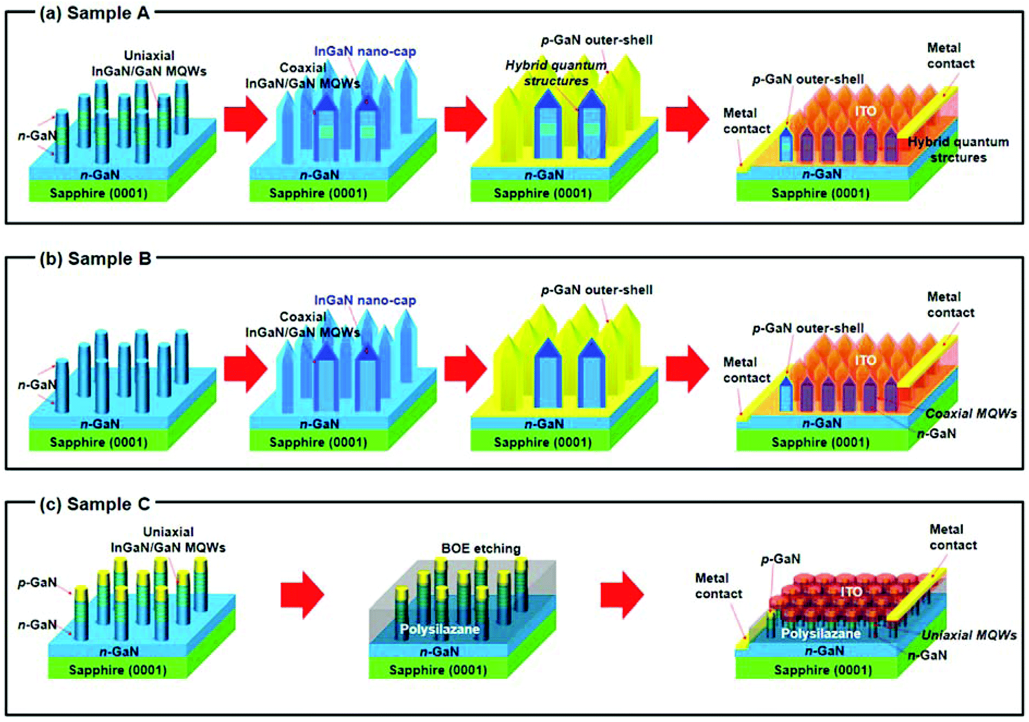 | ||
| Fig. 1 Schematic representation of fabrication process of photovoltaic devices using (a) hybrid nanostructure (sample A), (b) coaxial InGaN/GaN MQWs (sample B) and (c) uniaxial InGaN/GaN MQWs (sample C). | ||
2.3 Characterization
The surface morphology of the grown nanowires was characterized by employing a Hitachi S-7400 field emission-scanning electron microscope (FE-SEM) operated at 15 kV. The crystallinity was examined by a JEM-ARM-200F Cs-corrected-field emission transmission electron microscopy (Cs-corrected-FE-TEM) instrument equipped with EDX facility, at an accelerating voltage of 200 kV. InGaAs detector and He–Cd laser (λ = 325 nm) were used for the photoluminescence (PL) measurements at room temperature. Low temperature cathodoluminescence (LT-CL) spectra were taken at the applied accelerating voltage (Va) and beam current (Ib) 10 kV and 1000 pA, respectively. Photovoltaic measurements were carried under the standard AM 1.5 condition (light power density 100 mW cm−3) using K401 power supply (McScience Inc.) at room temperature.3. Results and discussion
FE-SEM was performed on the grown structures to characterize the surface morphology. Fig. 2(a–c) shows the FE-SEM images of fabricated NWs with uniaxial and hybrid MQW structures. Uniformly distributed, highly dense and nearly vertically aligned NWs can be seen in all the samples. Fig. 2(c) depicts the n-GaN/uniaxial InGaN/GaN MQWs/n-GaN NWs after ICP-RIE process. Diameter and length of the cylindrical shaped n-GaN/uniaxial InGaN/GaN MQWs/n-GaN NWs are 0.2 μm and 1 μm, respectively. Fig. 2(a) displays the FE-SEM image of n-GaN/uniaxial InGaN/GaN MQWs/n-GaN NWs after growing the coaxial InGaN/GaN MQWs and InGaN nano-cap layers. The diameter and length of the NWs of the hybrid nanostructure are in this case slightly increased to 0.24 μm and 1.2 μm, respectively. Interestingly, the NWs achieved a hexagonal structure along with a pyramidal tip exposing m- and r-planes, after growing the coaxial InGaN/GaN MQWs, as shown in the inset of Fig. 2(a). The surface morphology of sample B is nearly similar to the hybrid nanostructures, as shown in Fig. 2(b).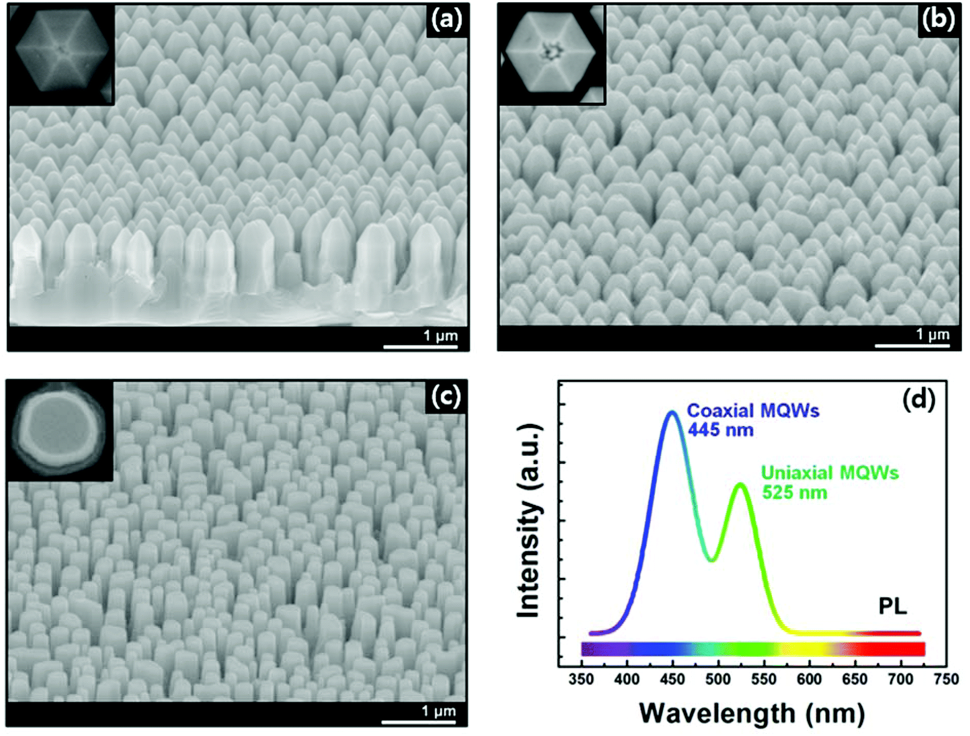 | ||
| Fig. 2 (a) FE-SEM image of hybrid nanostructure comprising uniaxial and coaxial InGaN/GaN MQWs and InGaN nano-cap; (b) FE-SEM image of coaxial InGaN/GaN MQWs nanowires; (c) FE-SEM image of uniaxial InGaN/GaN MQWs/n-GaN nanowires after ICP-RIE process; (d) PL spectra of the final hybrid nanostructure grown on n-GaN/uniaxial InGaN/GaN MQWs/n-GaN nanowires. | ||
The optical properties of the hybrid nanostructure InGaN/GaN MQWs were investigated by photoluminescence (PL) spectroscopy. Fig. 2(c) shows the PL spectra of the hybrid nanostructure recorded at room temperature. Two dominant peaks can be clearly observed in the blue region (445 nm) and green region (525 nm). The blue emission peak is attributed to coaxial InGaN/GaN MQWs, whereas the green emission peak is related to the uniaxial type MQWs. The PL spectrum shown in Fig. 2(c), which was carried out on the complete hybrid nanostructure; however the effect of InGaN nano-cap layer was not identified. Therefore, the optical properties of the hybrid nanostructure were studied in detail employing low temperature cathodoluminescence (LT-CL) point analysis.
Fig. 3(a) shows the FE-SEM image of a single hybrid nanostructure, which was subjected to LT-CL measurement at different points. Fig. 3(a) also displays various identified points (①, ②, ③ and ④) for recording LT-CL spectra along the length of nanowire. Fig. 3(b–e) represents the corresponding LT-CL spectra recorded at different points (as indicated in figure). In the LT-CL spectra obtained from point ① (Fig. 3(b)), showed a dominant peak at 500 nm along with very weak peak at 445 nm. The dominant green emission peak at 500 nm is attributed to InGaN nano-cap layer and the weak peak is originated from the coaxial InGaN/GaN MQWs. Full width half maximum (FWHM) for the InGaN nano-cap is 24.46 nm while the same for coaxial InGaN/GaN MQWs is 26.50 nm. The sharpness of the green emission peak in Fig. 3(b) can be attributed to homogeneous distribution of In over the InGaN nano-cap. Additionally, nearly defect free growth of InGaN nano-cap over the c-plane of n-GaN/uniaxial InGaN/GaN MQWs/n-GaN NWs also contributes to the narrow 500 nm green emission peak. Fig. 3(c and d) shows the LT-CL spectra measured at points ② and ③. It is seen that both the LT-CL spectra exhibit nearly similar features. The blue emission peak at 432 nm is the result of m-plane coaxial InGaN/GaN MQWs grown on n-GaN/uniaxial InGaN/GaN MQWs/n-GaN NWs while the green emission peak at 523 nm originates from uniaxial InGaN/GaN MQWs. The FWHMs for blue and green emissions are estimated to be 48.93 nm and 75.96 nm, respectively for the CL spectra recorded at point ②. The FWHMs of the CL spectra recorded at point ③ are calculated to be 53.38 nm and 61.16 nm for blue and green emission, respectively. In addition, a yellow tailing can be seen in both Fig. 3(c) and (d), which may be attributed to the formation of defects during the ICP-RIE process to fabricate the uniaxial InGaN/GaN MQWs. A strong and sharp GaN characteristic peak at 360 nm is noted in all the CL spectra recorded at different points. The In composition in the coaxial InGaN structure is estimated to be ∼15% (In0.15Ga0.85N). On the other hand, In composition in the uniaxial InGaN structure is ∼25% (In0.25Ga0.75N).
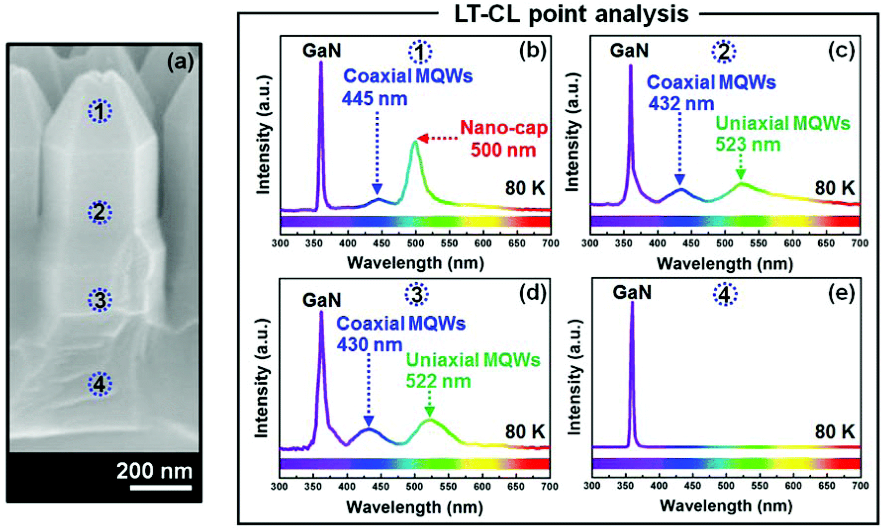 | ||
| Fig. 3 (a) FE-SEM image of single hybrid nanowire captured during low-temperature CL measurement at various spots (as indicated); (b) LT-CL spectra measured at ① showing emission from InGaN nano-cap and coaxial InGaN/GaN MQWs; (c) LT-CL spectra measured at ② showing emission from uniaxial and coaxial InGaN/GaN MQWs; (d) LT-CL spectra measured at ③ showing emission from uniaxial and coaxial InGaN/GaN MQWs; (e) LT-CL spectra measured at ④ showing n-GaN band edge emission. | ||
A Cs-corrected FE-TEM technique was employed in order to further analyze the insightful structural characteristics of realized hybrid nanostructures. Fig. 4(a) shows a single hybrid NW comprising uniaxial and coaxial InGaN/GaN MQWs with InGaN nano-cap. Fig. 4(a) also shows the spatial positions that correspond to the spot mode EDX spectra presented in Fig. 4(e–g). The high magnification FE-TEM images of coaxial, uniaxial InGaN MQWs and the InGaN nano-cap layer are shown in Fig. 4(b), (c) and (d), respectively. The barrier and the well structures of MQW were found to be very clear with regular intervals and the interface regions were reasonably sharp. From Fig. 4(b) it is seen that 6 pairs of InGaN/GaN MQWs coaxially grown on n-GaN nanowires. The InGaN well thickness and GaN barrier layer thickness were measured to be 2 nm and 5 nm, respectively. Five pairs of uniaxial InGaN/GaN MQWs grown on GaN and the thickness of the InGaN wells was about 4 nm, while GaN barriers were about 20 nm (Fig. 4(c)). High-magnified image of pyramidal shaped InGaN nano-cap layer is presented in Fig. 4(d) and the corresponding EDX profile is displayed in Fig. 4(g). The InGaN nano-cap was grown through inter-diffusion phenomenon during the growth of coaxial InGaN/GaN MQWs. During the growth of coaxial InGaN/GaN MQWs, In adatoms incorporated with Ga to form the pyramidal InGaN nano-cap. The growth process and mechanism of InGaN nano-cap layer have been previously reported.34 In this case also, the In atoms are homogeneously distributed over the InGaN nano-cap layer. These observations are well matched with the EDX elemental analysis and LT-CL spectra presented in Fig. 3.
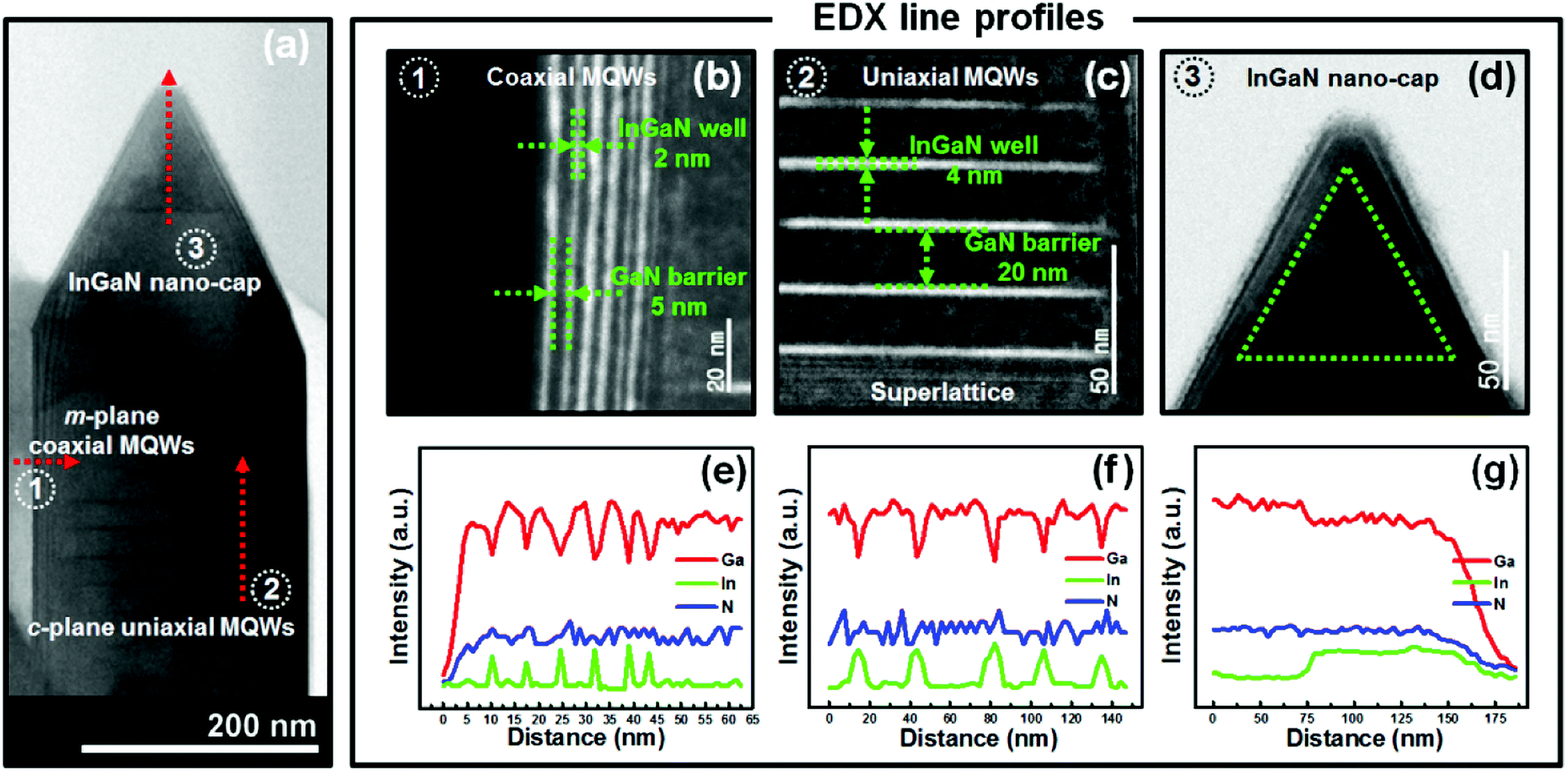 | ||
| Fig. 4 (a) Cs-corrected-FE-TEM image of the hybrid nanostructure showing uniaxial and coaxial InGaN/GaN MQWs along with InGaN nano-cap; (b) high magnified Cs-corrected-FE-TEM image of the coaxial InGaN/GaN MQWs showing well and barrier layer; (c) high magnified Cs-corrected-FE-TEM image of the uniaxial InGaN/GaN MQWs showing well and barrier layer; (d) high magnified Cs-corrected-FE-TEM image of the InGaN nano-cap; (e) EDX line profile for coaxial InGaN/GaN MQWs; (f) EDX line profile data for uniaxial InGaN/GaN MQWs; (g) EDX line profile data for InGaN nano-cap. | ||
In order to investigate the photovoltaic performance, solar cells have been fabricated with hybrid nanostructures and the device structure is schematically shown in Fig. 5(a). For the purpose of comparison photovoltaic devices also have been fabricated with uniaxial and coaxial InGaN/GaN MQW nanowires and schematic diagrams are shown in Fig. 5(b) and (c). Carrier collection at the electrode plays a crucial role in solar cell operations. In order to optimize the doping concentration in p-type GaN top layers, the device performance of hybrid nanostructure solar cells have been studied by varying the CP2Mg flow rates during the growth. The measured J–V characteristics of the hybrid nanostructure solar cells under 1 sun illumination at different CP2Mg flow rates are shown in Fig. 5(d). It is observed that with increase in CP2Mg flow rates from 4 to 20 sccm, the open circuit voltage (Voc) increases monotonously. Increase in CP2Mg flow rate results in high doping concentration in p-GaN leading to enhance the built-in potential and hence higher Voc.35,36 On the other hand, with increase in CP2Mg flow rates from 4 to 12 sccm, short-circuit current (Jsc) increases monotonously. Further increase in CP2Mg flow rate results in a substantial decrease in short-circuit current. Higher CP2Mg flow rate thus higher doping concentration causes the introduction of more impurity atoms and defects in the p-GaN, which greatly increases the scattering and carrier recombination leads to decrease in Jsc.37
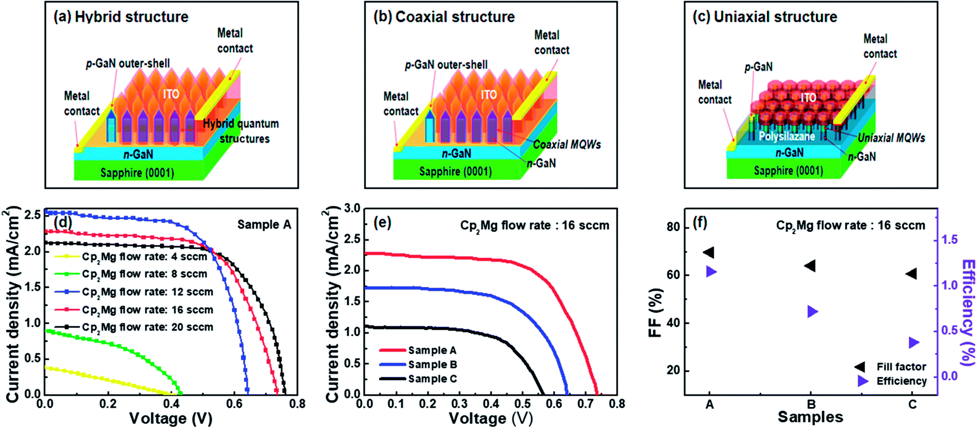 | ||
| Fig. 5 Schematic illustration of the photovoltaic devices fabricated with (a) hybrid InGaN/GaN MQWs, (b) coaxial InGaN/GaN MQWs, (c) uniaxial InGaN/GaN MQWs; (d) J–V curve of the photovoltaic devices fabricated with different InGaN/GaN MQWs architectures; (e) J–V curves of the fabricated hybrid nanostructure photovoltaic device with different CP2Mg flow rate; (f) FF and efficiency of the photovoltaic devices fabricated with different InGaN/GaN MQW architectures. | ||
The J–V characteristics of the photovoltaic devices fabricated with different InGaN/GaN MQW architectures under 1 sun illumination are shown in Fig. 5(e). The CP2Mg flow rate was fixed at 16 sccm for the deposition of p-GaN layers. The calculated device parameters are listed in Table 1. It is observed that the InGaN/GaN MQWs architecture has a significant effect in the performance of the fabricated photovoltaic devices. From a comparison with the device parameters listed in Table 1, it is seen that the device performance of solar cell fabricated with hybrid nanostructure is superior to the uniaxial as well as coaxial structures. The solar cell fabricated with hybrid nanostructures exhibits the high efficiency of 1.16% with short circuit current density (Jsc) of 2.28 mA cm2, open circuit voltage (Voc) of 0.73 mV and fill factor (FF) of 70%. It is also noticed that the open circuit voltages are slightly different but the short circuit currents strongly depends on the InGaN/GaN MQWs architectures. Therefore, it is believed that the photon absorption and hence the carrier generations in InGaN active area primarily determine the photovoltaic performance of the fabricated devices. The solar cell fabricated with uniaxial InGaN/GaN MQWs displays low efficiency (0.38%), arising from the poor performance due to the smaller InGaN active area. Coaxial InGaN/GaN MQWs based device shows an improvement in cell efficiency over uniaxial device increasing from 0.38% to 0.72%. The marginal improved device performance in the case of coaxial structure is attributed to the relatively large InGaN active area. Interestingly, the hybrid nanostructure device displays substantially enhanced cell efficiency of 1.16%, which is essentially arising from the significantly large InGaN active area due to the combination of uniaxial and coaxial InGaN/GaN MQWs. However, the operation mechanism of hybrid nanostructure based solar cells is not yet completely understood and subject to future study. A comparison of the photovoltaic parameters of the III-nitride nanowire based solar cells is listed in Table 2. It may be mentioned that the cell efficiency remains below the state-of-the-art values for InGaN/GaN MQW thin films based device. However, hybrid nanostructure device displays considerably better performance compared to the previously reported InGaN/GaN MQWs nanowire based solar cells. Therefore, it is inferred that the introduction of coaxial and uniaxial InGaN/GaN MQWs in hybrid nanostructure substantially enhanced the photon absorption and hence electron–hole pair generation leading to superior photovoltaic characteristics. The device performance of nanowire InGaN/GaN MQWs solar cell can be further improved by optimizing coaxial and uniaxial structures, barrier thickness, doping concentration in p-GaN layers, crystalline quality and the thickness of InGaN active area.
| Device type | Jsc (mA cm−2) | Voc (V) | FF (%) | Efficiency (%) |
|---|---|---|---|---|
| Sample A (hybrid MQWs) | 2.28 | 0.73 | 69.76 | 1.16 |
| Sample B (coaxial MQWs) | 1.75 | 0.64 | 64.19 | 0.72 |
| Sample C (uniaxial MQWs) | 1.10 | 0.56 | 60.86 | 0.38 |
| Sl no. | Device type | Voc | Jsc (mA cm−2) | FF | Efficiency | References |
|---|---|---|---|---|---|---|
| 1 | p-GaN:n-Si | 0.62 V | 4.40 | 38% | 2.73% | 31 |
| 2 | InN p-i-n | 0.13 V | 14.40 | 30% | 0.68% | 38 |
| 3 | n-GaN:n-Si | 0.35 V | 22.20 | — | 2.44% | 39 |
| 4 | p-GaN/InGaN/n-GaN | 0.22 V | 4.60 | 34% | 0.50% | 40 |
| 5 | p-InGaN core shell | 0.50 V | 1.00 |
54% | 0.30% | 41 |
| 6 | Coaxial InGaN/GaN MQWs | 0.68 V | 1.16 | 54% | 0.38% | 1 |
| 7 | Coaxial InGaN/GaN MQWs | 1.00 V | 0.39 | 56% | 0.19% | 42 |
| 8 | Coaxial InGaN/GaN MQWs | 0.95 V | 0.60 | 83% | 0.33% | 33 |
| 9 | Coaxial and uniaxial InGaN/GaN MQWs | 0.73 V | 2.28 | 70% | 1.16% | This work |
4. Conclusion
In conclusion, a hybrid nanostructure comprising uniaxial and coaxial InGaN/GaN MQWs nanowires is successfully realized and implemented in solar cell. The hybrid nanostructure consists of distinct uniaxial and coaxial InGaN/GaN MQWs along with InGaN nano-cap layer. The performance of the fabricated photovoltaic device strongly depends on the InGaN/GaN MQWs architecture. The solar cell fabricated with hybrid nanostructures comprising uniaxial and coaxial MQWs exhibits superior photovoltaic performance compared to the uniaxial as well as coaxial MQWs structures. The improved photovoltaic characteristics in hybrid nanostructure solar cell is primarily attributed to the larger InGaN active area leading to enhance the electron–hole pair generation, which results in high short-circuit current and hence higher cell efficiency. A conversion efficiency of 1.16% together with fill factor of 70% was obtained from the hybrid nanostructure solar cell. Doping concentration in p-type GaN top layer was varied by changing CP2Mg flow rate to study the performance of hybrid nanostructure based device. Higher doping concentration in p-GaN enhances the built-in potential and hence higher open-circuit voltage. The short-circuit current is also found to increase with increase in the p-type doping concentration. However, excessively high doping concentration causes the introduction of more impurity atoms and defects in the p-GaN, which greatly increases scattering and carrier recombination, results in decrease in short-circuit current. It is envisioned that the device performance of the nanowire InGaN/GaN MQWs solar cell can be further improved by optimizing coaxial and uniaxial structure, barrier thickness, doping concentration and crystalline quality of InGaN active area. In spite of inferior achieved efficiency, this novel hybrid nanostructure InGaN/GaN MQWs nanowire device with large active area provides a plausible alternative direction to improve the performance of next generation III-nitrides nanowire based photovoltaic devices.Conflicts of interest
The authors declare no conflict of interest.Acknowledgements
This work was supported by the National Research Foundation of Korea (NRF) grant funded by the Korea government (MSIP) (No. 2015R1A2A2A01002877) and (No. 2015R1A4A1042417).References
- Y.-J. Li, Y. L. Tsail, J.-R. Chang, S.-P. Chang, C.-C. Lin, Y.-J. Cheng, H.-C. Kuo, P. Yu and C.-Y. Chang, in Photovoltaic Specialist Conference (PVSC), IEEE 42nd, IEEE, 2015, pp. 1–3 Search PubMed.
- J. J. Wierer, Q. Li, D. D. Koleske, S. R. Lee and G. T. Wang, Nanotechnology, 2012, 23, 194007 CrossRef PubMed.
- A. G. Bhuiyan, K. Sugita, A. Hashimoto and A. Yamamoto, IEEE J. Photovolt., 2012, 2, 276–293 CrossRef.
- R. Dahal, B. Pantha, J. Li, J. Y. Lin and H. X. Jiang, Appl. Phys. Lett., 2009, 94, 63505 CrossRef.
- R. Dahal, J. Li, K. Aryal, J. Y. Lin and H. X. Jiang, Appl. Phys. Lett., 2010, 97, 73115 CrossRef.
- Y. Kuwahara, T. Fujii, T. Sugiyama, D. Iida, Y. Isobe, Y. Fujiyama, Y. Morita, M. Iwaya, T. Takeuchi, S. Kamiyama, I. Akasaki and H. Amano, Appl. Phys. Express, 2011, 4, 4–7 Search PubMed.
- M. Mori, S. Kondo, S. Yamamoto, T. Nakao, M. Iwaya, T. Takeuchi, S. Kamiyama, I. Akasaki and H. Amano, Jpn. J. Appl. Phys., 2013, 52, 08JH02 CrossRef.
- D. H. Lien, Y. H. Hsiao, S. G. Yang, M. L. Tsai, T. C. Wei, S. C. Lee and J. H. He, Nano Energy, 2015, 11, 104–109 CrossRef.
- B. O. Jung, S. Y. Bae, S. Y. Kim, S. Lee, J. Y. Lee, D. S. Lee, Y. Kato, Y. Honda and H. Amano, Nano Energy, 2015, 11, 294–303 CrossRef.
- J. Wu, W. Walukiewicz, K. M. Yu, W. Shan, J. W. Ager, E. E. Haller, H. Lu, W. J. Schaff, W. K. Metzger and S. Kurtz, J. Appl. Phys., 2003, 94, 6477–6482 CrossRef.
- G. Meneghesso, G. Verzellesi, F. Danesin, F. Rampazzo, F. Zanon, A. Tazzoli, M. Meneghini and E. Zanoni, IEEE Trans. Device Mater. Reliab., 2008, 8, 332–343 CrossRef.
- J. Wu, J. Appl. Phys., 2009, 106, 011101 CrossRef.
- X. Zhang, X. Wang, H. Xiao, C. Yang, J. Ran, C. Wang, Q. Hou and J. Li, J. Phys. D: Appl. Phys., 2007, 40, 7335–7338 CrossRef.
- X. Zhang, X. Wang, H. Xiao, C. Yang, J. Ran, C. Wang, Q. Hou, J. Li and Z. Wang, J. Phys. D: Appl. Phys., 2008, 41, 245104 CrossRef.
- L. Hsu and W. Walukiewicz, J. Appl. Phys., 2008, 104, 024507 CrossRef.
- B.-T. Tran, E.-Y. Chang, H.-D. Trinh, C.-T. Lee, K. C. Sahoo, K.-L. Lin, M.-C. Huang, H.-W. Yu, T.-T. Luong, C.-C. Chung and C.-L. Nguyen, Sol. Energy Mater. Sol. Cells, 2012, 102, 208–211 CrossRef.
- O. Jani, I. Ferguson, C. Honsberg and S. Kurtz, Appl. Phys. Lett., 2007, 91, 132117 CrossRef.
- N. G. Young, R. M. Farrell, Y. L. Hu, Y. Terao, M. Iza, S. Keller, S. P. Denbaars, S. Nakamura and J. S. Speck, Appl. Phys. Lett., 2013, 103, 173903 CrossRef.
- N. G. Young, E. E. Perl, R. M. Farrell, M. Iza, S. Keller, J. E. Bowers, S. Nakamura, S. P. Denbaars and J. S. Speck, Appl. Phys. Lett., 2014, 104, 163902 CrossRef.
- Y. Kuwahara, T. Fujii, T. Sugiyama, D. Iida, Y. Isobe, Y. Fujiyama, Y. Morita, M. Iwaya, T. Takeuchi, S. Kamiyama, I. Akasaki and H. Amano, Appl. Phys. Express, 2011, 4, 21001 CrossRef.
- S. Yamamoto, M. Mori, Y. Kuwahara, T. Fujii, T. Nakao, S. Kondo, M. Iwaya, T. Takeuchi, S. Kamiyama, I. Akasaki and H. Amano, Phys. Status Solidi RRL, 2012, 6, 145–147 CrossRef.
- K. Y. Lai, G. J. Lin, Y. L. Lai, Y. F. Chen and J. H. He, Appl. Phys. Lett., 2010, 96, 81103 CrossRef.
- S. Valdueza-felip, A. Mukhtarova, Q. Pan, G. Altamura, L. Grenet, C. Durand, J. Eymery, E. Monroy, C. Bougerol, D. Peyrade and F. Gonza, Jpn. J. Appl. Phys., 2013, 52, 08JH05 CrossRef.
- N. Watanabe, M. Mitsuhara, H. Yokoyama, J. Liang and N. Shigekawa, Jpn. J. Appl. Phys., 2014, 53, 112301 CrossRef.
- A. Mukhtarova, S. Valdueza-Felip, L. Redaelli, C. Durand, C. Bougerol, E. Monroy and J. Eymery, Appl. Phys. Lett., 2016, 108, 161907 CrossRef.
- J. Zhu, Z. Yu, G. F. Burkhard, C. M. Hsu, S. T. Connor, Y. Xu, Q. Wang, M. McGehee, S. Fan and J. Cui, Nano Lett., 2009, 9, 279–282 CrossRef PubMed.
- E. C. Garnett, M. L. Brongersma, Y. Cui and M. D. McGehee, Annu. Rev. Mater. Res., 2011, 41, 269–295 CrossRef.
- B. M. Kayes, H. A. Atwater and N. S. Lewis, J. Appl. Phys., 2005, 97, 114302 CrossRef.
- Z. Yu, A. Raman and S. Fan, Proc. Natl. Acad. Sci. U. S. A., 2010, 107, 17491–17496 CrossRef PubMed.
- Y. J. Dong, B. Z. Tian, T. J. Kempa and C. M. Lieber, Nano Lett., 2009, 9, 2183–2187 CrossRef PubMed.
- Y. B. Tang, Z. H. Chen, H. S. Song, C. S. Lee, H. T. Cong, H. M. Cheng, W. J. Zhang, I. Bello and S. T. Lee, Nano Lett., 2008, 8, 4191–4195 CrossRef PubMed.
- M. F. Cansizoglu, S. M. Hamad, D. P. Norman, F. Keles, E. Badraddin, T. Karabacak and H. W. Seo, Appl. Phys. Express, 2015, 8, 1–4 Search PubMed.
- A. Messanvi, H. Zhang, V. Neplokh, F. H. Julien, F. Bayle, M. Foldyna, C. Bougerol, E. Gautier, A. Babichev, C. Durand, J. Eymery and M. Tchernycheva, ACS Appl. Mater. Interfaces, 2015, 7, 21898–21906 Search PubMed.
- J.-H. Park, U. Chatterjee, S. Kang, K. Lee, J.-S. Kim and C.-R. Lee, J. Mater. Chem. C, 2016, 4, 10005–10010 RSC.
- L. Zhang, H.-L. Shen, Z.-H. Yue, F. Jiang, T.-R. Wu and Y.-Y. Pan, Chin. Phys. B, 2013, 22, 16803 CrossRef.
- M. Yao, N. Huang, S. Cong, C. Chi, M. A. Seyedi, Y. Lin, Y. Cao, M. L. Povinelli, P. D. Dapkus and C. Zhou, Nano Lett., 2014, 14, 3293–3303 CrossRef PubMed.
- G. F. Brown, J. W. Ager, W. Walukiewicz and J. Wu, Sol. Energy Mater. Sol. Cells, 2010, 94, 478–483 CrossRef.
- H. P. T. Nguyen, Y. L. Chang, I. Shih and Z. Mi, IEEE J. Sel. Top. Quantum Electron., 2011, 17, 1062–1069 CrossRef.
- A. M. Mozharov, A. D. Bolshakov, D. A. Kudryashov, N. V. Kryzhanovskaya, G. E. Cirlin, I. S. Mukhin, J. C. Harmand and M. Tchernysheva, J. Phys.: Conf. Ser., 2015, 643, 2–8 CrossRef.
- M. F. Cansizoglu, S. M. Hamad, D. P. Norman, F. Keles, E. Badraddin, T. Karabacak and H. W. Seo, Appl. Phys. Express, 2015, 8, 42302 CrossRef.
- J. J. Wierer, Q. Li, D. D. Koleske, S. R. Lee and G. T. Wang, Nanotechnology, 2012, 23, 194007 CrossRef PubMed.
- Y. J. Dong, B. Z. Tian, T. J. Kempa and C. M. Lieber, Nano Lett., 2009, 9, 2183–2187 CrossRef PubMed.
| This journal is © The Royal Society of Chemistry 2018 |