
 Open Access Article
 This Open Access Article is licensed under a Creative Commons Attribution-Non Commercial 3.0 Unported Licence
Precision excimer laser annealed Ga-doped ZnO electron transport layers for perovskite solar cells†
Rui Xiaab,
Guangyue Yinac,
Shimao Wang ad,
Weiwei Dong*ad,
Libing Youa,
Gang Mengad,
Xiaodong Fang*acd,
Mohammad Khaja Nazeeruddinb,
Zhaofu Feib and
Paul J. Dyson*b
ad,
Weiwei Dong*ad,
Libing Youa,
Gang Mengad,
Xiaodong Fang*acd,
Mohammad Khaja Nazeeruddinb,
Zhaofu Feib and
Paul J. Dyson*b
aAnhui Provincial Key Laboratory of Photonic Devices and Materials, Anhui Institute of Optics and Fine Mechanics, Chinese Academy of Sciences, Hefei 230031, China. E-mail: wwdong@aiofm.ac.cn; xdfang@aiofm.ac.cn
bInstitut des Sciences et Ingénierie Chimiques, Ecole Polytechnique Fédérale de Lausanne (EPFL), CH-1015 Lausanne, Switzerland. E-mail: paul.dyson@epfl.ch
cUniversity of Science and Technology of China, Hefei 230026, China
dKey Laboratory of Photovoltaic and Energy Conservation Materials, Chinese Academy of Sciences, Hefei 230031, China
First published on 15th May 2018
Abstract
Organic–inorganic hybrid perovskite solar cells (PSCs) continue to attract considerable attention due to their excellent photovoltaic performance and low cost. In order to realize the fabrication of PSCs on temperature-sensitive substrates, low-temperature processing of all the components in the device is required, however, the majority of the high-performance PSCs rely on the electron transport layers (ETLs) processed at high temperatures. Herein, we apply excimer laser annealing (ELA) to treat ETLs (Ga-doped ZnO, GZO) at room temperature. A synergetic improvement in optical transparency and electrical conductivity is achieved after ELA treatment, which in turn improves light absorption, enhances electron injection, and depresses charge recombination. Devices fabricated with ELA treated GZO ETL acheived a power conversion efficiency (PCE) of 13.68%, higher than that of the PSCs utilizing GZO with conventional high-temperature annealing (12.96%). Thus, ELA is a promising technique for annealing ETLs at room temperature to produce efficient PSCs on both rigid and flexible substrates.
Introduction
By employing organic–inorganic hybrid perovskite materials as light harvesters with a suitable band gap,1 high absorption coefficient and carrier mobility,2,3 small exciton binding energy,4 and long exciton diffusion length,5 perovskite solar cells (PSCs) have become key players in the field of photovoltaics. By optimizing the device architecture and composition of the perovskite materials, the power conversion efficiency (PCE) of PSCs has improved from 3.8 to 22.7%.6–10 In most of PSCs, the electron transport layer (ETL) is an indispensable component in improving electron extraction and blocking the holes.11,12High transmittance and electrical conductivity are required for an ideal ETL and, to date, TiO2 is the most widespread ETL material employed in PSCs with high PCEs.13–15 However, for both planar heterojunction and mesoporous structured PSCs, the TiO2 layers require sintering at high temperatures (450–550 °C) to increase crystallinity and mobility, which inevitably increases fabrication costs while also hindering the development of flexible PSCs.16
Excimer laser annealing (ELA) has been extensively used to transform amorphous silicon into poly-silicon on an industrial scale. It is an efficient method to achieve fast and complete crystallization of films at room temperature with little peripheral damage which leads to improved photoelectric properties.17,18 Basically, when excimer lasers with different wavelengths (193–351 nm) irradiate the films, the laser energy needs to be absorbed efficiently in order to rapidly convert the light energy to heat.
Herein, Ga-doped ZnO was selected as the ETL treated by ELA technique in planar structured PSC due to two main reasons. First, ZnO is a proper electron transport material with a suitable work function, high electron conductivity, and the potential to be prepared at ambient temperatures.19 By doping ZnO with group III elements such as Al and Ga, the electrical conductivity and stability of ZnO can be further modified.20,21 Ga ions are particularly suitable dopants as their size is similar to that of Zn ions, which results in smaller lattice deformation even at high dopant concentrations.22,23 Second, ZnO has a high intrinsic absorption coefficient to UV laser light allowing excimer laser energy to be absorbed easily by superficial films, leading to a sharp rise of temperature and causing a beneficial heating effect lasting for dozens of nanoseconds and inducing fast crystallization.24–26 To date, 248 nm and 308 nm excimer laser have been successfully used to treat ZnO films and Al doped ZnO films at room temperature, resulting in improved transparency and conductivity due to the enhanced crystallization.27–29 Moreover, since the thickness of ETLs used in PSCs is usually in the order of a few dozen nanometers,30 ELA technique is expected to be a suitable and cost-effective method to improve the optoelectronic properties of ETLs at room temperature.
In this paper, we describe the application of ELA technique with XeCl excimer laser (308 nm) to treat GZO films and, subsequently, applying them as ETLs in planar heterojunction PSCs (PHJ-PSCs). By optimizing the fluence and the pulse counts of the laser irradiation, it was possible to decrease the films resistivity by 4 orders of magnitude with improved transmittance, and the thermal stability of methylammonium lead triiodide (MAPbI3) on the ELA treated GZO film was also enhanced. Simulations of the ELA process were employed to investigate the temporal and spatial temperature field upon one laser pulse, and showed that the method causes little damage to the substrate. A comparison of PSCs fabricated with GZO ETLs prepared by conventional heat treatment and ELA treatment demonstrates the latter to have a better photovoltaic performance due to improved light absorption, enhanced electron injection, and reduced charge recombination.
Experimental
Preparation of the GZO films
The GZO films were deposited from a GZO target (purchased from Zhongnuo material Co., Ltd. China) on FTO substrates by RF magnetron sputtering at room temperature. Before sputtering, the substrates were ultrasonically cleaned with distilled water, acetone, and ethanol, respectively. The atomic ratio of Ga to Zn in the GZO film is 5![[thin space (1/6-em)]](https://www.rsc.org/images/entities/char_2009.gif) :95. Before deposition, the pressure in chamber was adjusted to 4 × 10⁻⁴ Pa, high purity (99.999%) Ar gas with 30 sccm was introduced through a mass flow controller. During the deposition, the chamber pressure, RF power, and deposition time were adjusted to be 0.6 Pa, 100 W, and 2 min, respectively.
:95. Before deposition, the pressure in chamber was adjusted to 4 × 10⁻⁴ Pa, high purity (99.999%) Ar gas with 30 sccm was introduced through a mass flow controller. During the deposition, the chamber pressure, RF power, and deposition time were adjusted to be 0.6 Pa, 100 W, and 2 min, respectively.
Excimer laser annealing treatment
GZO films were laser-annealed by irradiating the surface of the film with a XeCl (308 nm) excimer laser in air at room temperature. The thickness of the films were measured with a step profiler and found to be approximately 36 nm, a schematic of the excimer laser anneal system is shown in Fig. 1. A laser beam with an energy of 200 mJ was irradiated onto the films after focussing. The repetition rate of the laser pulse is 1 Hz. The energy density can be calculated by dividing the laser energy by the irradiating area. By adjusting the distance between the film and focusing lens, the effective area changes, thus different energy densities of 105, 90, 75, and 60 mJ cm−2 were obtained. The pulse count was adjusted to 1, 5, 10, 20, 30, and 40, respectively. The samples under different treatment conditions are labelled as ELA (energy density)-(pulse number). The as-prepared GZO films without any treatment (NG) as well as heated to 500 °C in air (HG), prepared according to pervious report,31 were employed for comparison. To ensure the reproducibility for the data 6 samples are included in each group.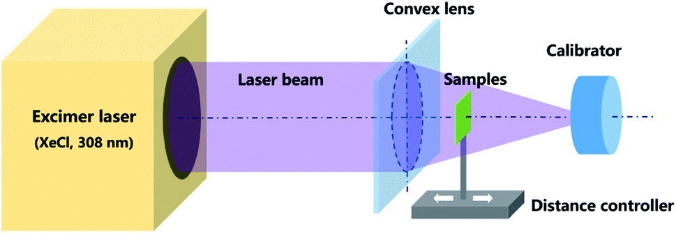 | ||
| Fig. 1 Schematic depicting the ELA system applied to GZO films. | ||
Fabrication of hetero-junction perovskite solar cells
The GZO films with different treatments were used as ETLs in PHJ-PSC. One-step method was applied for the fabrication of the perovskite layer. Specifically, PbI2 (477 mg) and methylammonium iodide (MAI, 160 mg) were dissolved in N,N-dimethylformamide (DMF, 0.64 mL) and N,N-dimethylsulfoxide (DMSO, 0.16 mL) to form the precursor solution. The solution (40 μL) was spin-coated on the GZO films at 1000 rpm for 3 s, then 4000 rpm for 12 s, chlorobenzene (CB, 0.3 mL) was uniformly dripped onto the rotating substrate in 10 s at 4000 rpm. The formed MAPbI3 films were heated at 70 °C for 10 min. The hole transport layer (solution of Spiro-OMeTAD in chlorobenzene with additive according to the previous report32) was spin-coated on the MAPbI3 films at 4000 rpm for 30 s. Finally, 60 nm of Au electrode was deposited on the hole transport layer via vacuum thermal evaporation. For comparison, ZnO ETLs prepared by magnetron sputtering (HZ) followed by 500 °C of heat treatment were also used to fabricate PHJ-PSCs employing the same fabrication process.Characterization
The crystal structure of the films was investigated by X-ray diffraction (XRD, Philips X'pert diffractometer, Holland) with Cu Kα radiation (λ = 1.5418 Å). The morphology of the films was determined using a field-emission scanning electron microscope (FE-SEM, FEI Sirion-200, USA) and an atomic force microscope (AFM, CSPM-5500, China). A step profiler (XP-2, AMBIOS Technology Inc., USA) was used to measure the film thickness. The optical transmittance and absorption spectra of the films were determined by UV-visible spectrophotometry (U-3900H, Japan) in the wavelength range 200 to 900 nm. The resistivity was measured by the standard four probe d.c. method using a Keithley 2420 digital source meter.The photocurrent–photovoltage (J–V) curves of the PHJ-PSCs were measured with a Keithley 2420 digital source meter under irradiation of a solar simulator (Newport Oriel 94043A, USA, AM 1.5, 100 mW cm−2). The monochromatic incident photon to electron conversion efficiency (IPCE) spectra were determined employing a 300 W Xe lamp light source with monochromatic light in the range 300 to 900 nm. Electrochemical impedance spectroscopy (EIS) was conducted on a frequency response analyzer (Zahner, Zennium, Germany), the cells were measured under the bias voltages of 0.8 V in the dark, the frequency range was 1 to 106 Hz, and the magnitude of the alternative signal was 10 mV. The photoluminescence (PL) spectra of the perovskite films were obtained using an Edinburgh FLSP920 spectrometer (UK) with an excitation xenon lamp source. The transient absorption spectra (TAS) of the perovskite films were acquired using laser flash photolysis spectrophotometry (LKS80, UK), the energy of the laser device was 150 mJ cm−2 and the repetition rate was 5 Hz. The wavelength of the excitation and probe light were 473 and 770 nm, respectively.
Simulations of the ELA process
Simulations of the ELA process was performed using ANSYS® software. The irradiation area of the incident light is large than the substrate and the absorbed power transferred from the laser is symmetrically distributed along the axial axis.Therefore, the model can be regarded as a heat flux caused by laser irradiation on a two dimensional finite element film along the thickness orientation, building on the basis that the phase transition does not take place. The thickness of the films and glass substrate was set as 36 nm and 360 nm, respectively. The energy of laser beam is viewed as the absorption in the form of heat, which follows a top Gauss distribution, and the relation between the heat flux and energy density can be described as follows:
| Q = (1 − R) × E/P | (1) |
Results and discussion
Properties of the GZO films prepared using ELA
A series of GZO films were prepared using different ELA treatments, termed ETL X-Y, where X = the fluence, Y = the pulse counts (see Experimental). The resistivity values of these GZO films are shown in Table 1 and Fig. 2(a). The average resistivity of the as-prepared film is 71.98 ± 1.05 Ω cm, after heat annealing at 500 °C, the resistivity is 0.12 ± 0.01 Ω cm. For ELA treatments, both of the fluence and the pulse counts were varied. The resistivity of the ELA-treated films with fluences of 60, 75, and 90 mJ cm−2 is reduced by 1 to 4 orders with pulse counts of 1 to 20. Further adding the counts to 30 and 40 lead to a slight increase of resistivity. According to the previous report, this phenomenon can be attributed to the UV laser treatment influencing the activation of Ga dopants and oxygen vacancies in ZnO based materials which act as electron donors.33–37 When the energy density is fixed at 105 mJ cm−2, the films are damaged by the second pulse count (Fig. S1†), therefore they are not able to get valid data. As a result, the resistivity of ELA 90-20 is observed to be the minimum value (0.018 ± 0.003 Ω m), which is much smaller than the value of samples with thermally annealed films, showing the superiority of the ELA technique over conventional heat treatment in optimizing the electrical property.| Fluence (mJ cm−2) | Pulse count | Resistivity (Ω cm) |
|---|---|---|
| 0 | 0 | 71.98 ± 3.48 |
| 60 | 1 | 59.97 ± 2.65 |
| 5 | 9.05 ± 0.89 | |
| 10 | 1.15 ± 0.11 | |
| 20 | 0.17 ± 0.02 | |
| 30 | 0.19 ± 0.01 | |
| 40 | 0.19 ± 0.02 | |
| 75 | 1 | 13.90 ± 1.05 |
| 5 | 0.22 ± 0.04 | |
| 10 | 0.093 ± 0.015 | |
| 20 | 0.031 ± 0.008 | |
| 30 | 0.033 ± 0.005 | |
| 40 | 0.035 ± 0.006 | |
| 90 | 1 | 10.45 ± 0.97 |
| 5 | 0.190 ± 0.03 | |
| 10 | 0.072 ± 0.02 | |
| 20 | 0.018 ± 0.003 | |
| 30 | 0.022 ± 0.004 | |
| 40 | 0.024 ± 0.006 | |
| 105 | 1 | 23.02 ± 1.02 |
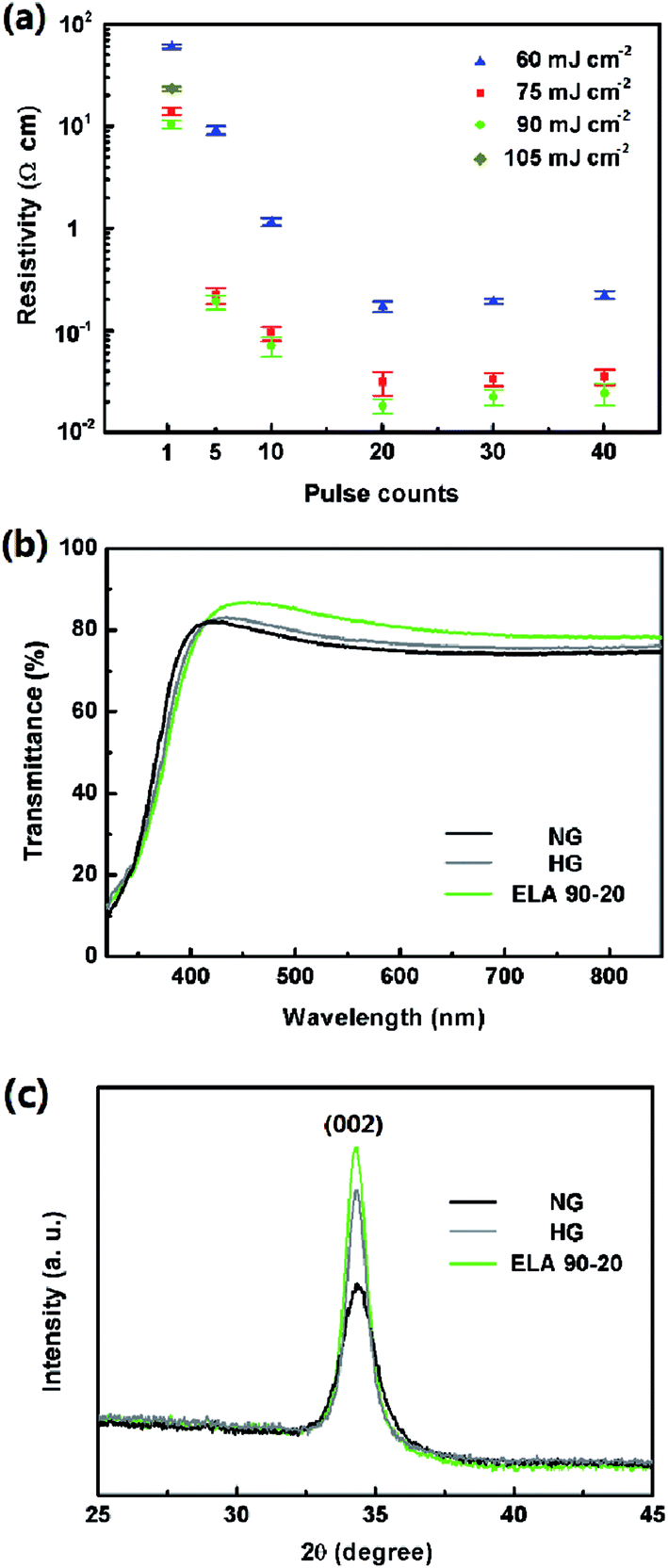 | ||
| Fig. 2 (a) Variation of resistivity of ELA-treated GZO films with pulse counts (1, 5, 10, 20, and 40) under fluence at 60, 75, 90, and 105 mJ cm−2. (b) Transmittance spectra and (c) XRD patterns of NG, HG, and ELA 90-20 on glass. | ||
Ideal ETLs are expected to have a high transmittance in UV-visual range. Transmittance of GZO films with different treatment was also evaluated, when the fluence is fixed at 90 mJ cm−2, increasing the pulse counts from 1 to 20 helps to increasing the overall transmittance, when the pulse counts reaches to 30 and 40, the transmittance slightly decreases (see Fig. S2a†). Altering the laser fluence from 60 mJ cm−2 to 90 mJ cm−2 and keeping the pulse counts at 20, i.e. ELA 90-20, the highest transmittance is observed (see Fig. S2b†). Compared with NG and HG, demonstrate in Fig. 2(b), it can be concluded that the ELA treatment is more effective than heat treatment in enhancing the transparency of the films. The optical bandgap (Eg) can be estimated from the absorption edge by Tauc's relation38 (A is the optical transition dependent constant, α is the absorption coefficient, and hν is the photon energy):
| (αhv)2 = A(hv − Eg)2 | (2) |
The bandgap of ELA 90-20 (3.44 eV) is larger than that of NG (3.31 eV) and HG (3.33 eV) (Fig. S2c†), and the blue shift may be attributed to the higher electron density associated with Burstein-Moss shift, which contributes to its lower electrical resistivity.39,40
The XRD patterns of the films after the ELA treatments with different fluence and pulse counts are shown in Fig. S3(a and b),† there is only one strong (002) diffraction peak, which indicates that all the GZO films are highly c-oriented and the gallium ions mainly play the role of a substitutional impurity in the wurtzite ZnO lattice.41,42 Increasing the pulse counts with the fluence fixed at 90 mJ cm−2 and the fluence when the pulse counts are fixed at 20 enhances the crystallinity. When comparing the ELA 90-20 with NG and HG films, it can be observed from Fig. 2(c) that the intensity of the (002) peak of the ELA 90-20 is the highest, which indicates that the ELA 90-20 treatment leads to a better crystallization effect than heat treatment.
The surface SEM images of the substrate and films prepared with different treatments are shown in Fig. 3, with the corresponding AFM images in the insets. The NG and HG GZO films are very similar whereas the ELA 90-20 film is compose of larger crystals, indicating that the ELA treatment effectively enlarges the grain size, which is in agreement with the XRD data. Moreover, the root mean square roughness (RMS) value after heat annealing and ELA 90-20 treatments increases from 14.3 nm (no treatment) to 16.9 nm and 16.4 nm, respectively, presumably because the thermal or laser treatments cause growth along a preferential orientation or cause adjacent grains to condense,43,44 as a result, the surface roughness increases and becomes more crystalline. This observation is in accordance with a previous report describing the use of lasers to crystalize AZO films.45 However, increasing the pulses counts to 30 (ELA 90-30) or fluence to 105 mJ cm−2 (ELA 105-1 and ELA 105-5), cracks appears on the film surface (see Fig. S1†). Thus, the ELA treatment enhances the conductivity and transparency of the GZO films, due to improvements in crystallinity and surface structure, but when loading more pulses counts or at higher fluence, the films are partly damaged, and the conductivity and transmittance decreases.
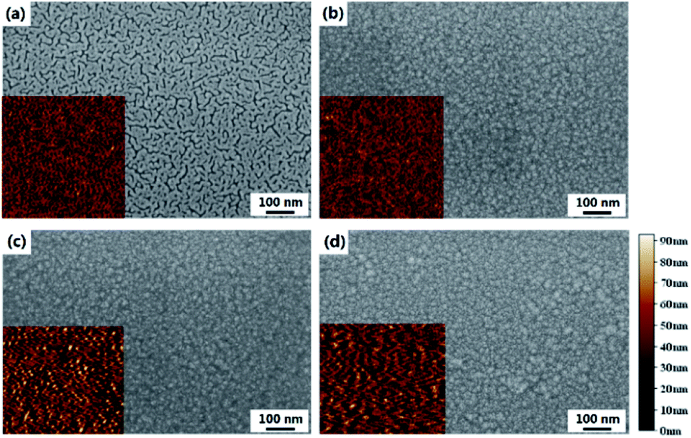 | ||
| Fig. 3 SEM images of (a) glass substrate, (b) NG, (c) HG, and (d) ELA 90-20, the inset is the corresponding AFM image. | ||
Simulation of the ELA process
To understand the origin of the change in films and the temperature field distribution after ELA treatment, ANSYS® software was used to simulate the ELA process to model the transient temperature field distributions in the different GZO films (see Experimental). As seen from Fig. 4(a), when the film is loaded under fluence of 90 mJ cm−2 for 1 pulse, the temperature of the film surface (Ts) reaches to 1918.1 °C, depicted in Fig. 4(b), this value is close to the melting point (1975 °C),46 which could facilitate the recrystallization of the films. It is worth mentioning that the temperature of the substrate is around 46 °C, inferring that laser irradiation causes little damage to the substrate, which is important for fabricating ETLs on temperature sensitive substrates. Fig. S4† shows the variation of the surface temperature with time from 0 to 100 ns as a function of the fluence. The temperature increases sharply in the initial 20 ns and then drops rapidly due to air convection. As the fluence increases from 60 to 105 mJ cm−2 the temperature rises faster, which results in the destruction of the films.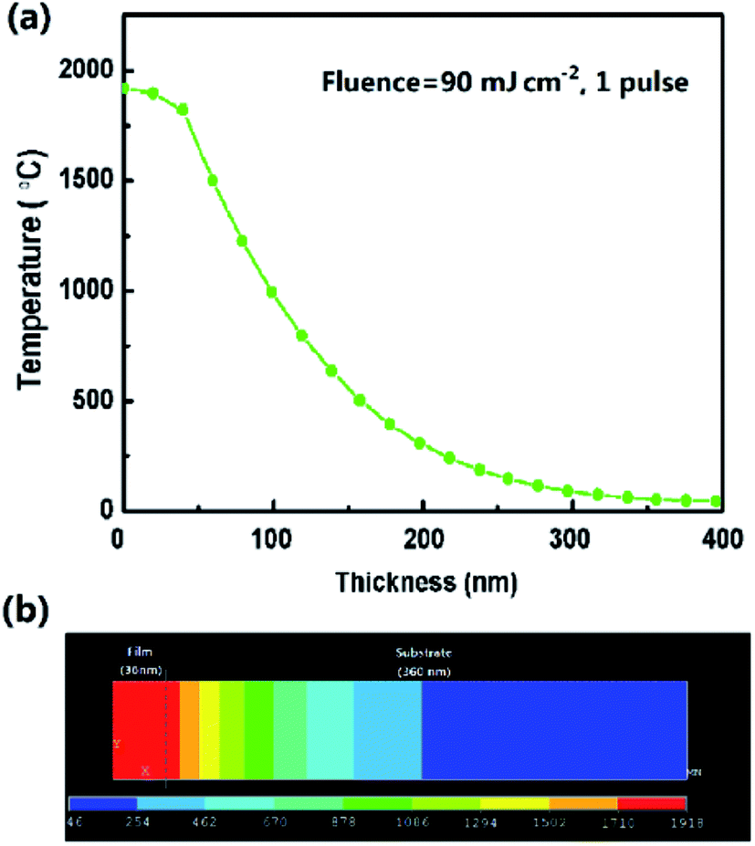 | ||
| Fig. 4 (a) Temperature distribution along the film thickness when loading fluence of 90 mJ cm−2 for 1 pulse (20 ns). (b) Temperature distribution in two dimensions model of ELA 90-20 at 20 ns. | ||
Cell performance
ELA 90-20 was selected as the ETL for use in PSCs and compared with PSCs containing NG and HG ETLs. The surface SEM image of the perovskite (MAPbI3) layer deposited on the ELA 90-20 is shown in Fig. 5(a). The MAPbI3 layer has a smooth surface with few voids and completely covers the ELA 90-20 film. The thickness of the MAPbI3 film is about 350 nm and the average diameter of the MAPbI3 grains is about 300 nm. The cross-section SEM image of the ELA 90-20 fabricated cell (Fig. 5(c)) shows that the ELA 90-20 film has a thickness of about 36 nm and is uniform, effectively preventing contact between the FTO and perovskite layer. Fig. 5(b) shows the XRD pattern of the FTO/ELA 90-20/MAPbI3 film. The peak at 34.2° is related to GZO, the peak at 34.2° corresponds to the GZO, and the diffraction peaks at 14.2, 28.5°, 31.9, 40.7 and 43.2° may be assigned to (110), (220), (310), (224) and (330) planes of the tetragonal MAPbI3 phase.47 The remaining peaks are consistent with FTO substrate. The characteristic peaks of PbI2 are not observed, which indicates that the quality and purity of the MAPbI3 is high.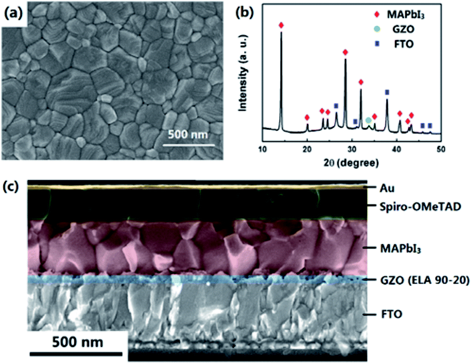 | ||
| Fig. 5 (a) SEM image of MAPbI3 layer on ELA 90-20. (b) XRD pattern of the MAPbI3 film prepared on the ELA 90-20 at FTO substrate. (c) Cross-sectional SEM image of the cell employing ELA 90-20. | ||
The J–V curves and corresponding parameters (short-circuit current density, Jsc. open-circuit voltage, Voc. fill factor, FF) of the fabricated PSCs are shown in Fig. 6(a) and listed in Table 2. The PCE of the device obtained from the reverse scan using the ELA 90-20 film is 13.68% (Jsc = 20.01 mA cm−2, Voc = 1.02 V, FF = 0.670) corresponding to a PCE of 11.73% (Jsc = 19.74 mA cm −2, Voc = 1.00 V, FF = 0.594) obtained from the forward scan (Fig. S5†), which is higher than that of the devices containing HZ (11.09%, Jsc = 18.29 mA cm−2, Voc = 0.95 V, FF = 0.638), NG (9.33%, Jsc = 17.18 mA cm−2, Voc = 0.91 V, FF = 0.60), and HG (12.96%, Jsc = 18.95 mA cm−2, Voc = 0.99 V, FF = 0.691). This difference may be attributed to the higher Jsc and Voc values as the light-harvesting-efficiency (LHE) of the MAPbI3 film on the ELA 90-20 ETL is the highest, i.e. from the IPCE spectrum shown in Fig. 6(b), the IPCE value of the cell containing ELA 90-20 is the highest between 300 and 800 nm. Based on the AM 1.5 G light spectrum, the integrated photocurrent density of the PSCs employing HZ, NG, HG, and ELA 90-20 were calculated to be 17.90, 16.91, 18.78, and 19.72 mA cm−2, respectively, which matches well with the Jsc values from the J–V curves. According to above-mentioned opto-electrical properties, the transmittance of the GZO films is improved after ELA treatment and the transparency of ELA 90-20 is the highest. A higher transmittance facilitates the absorption of the photo flux by the MAPbI3 layer, thus more photo-generated electrons are produced, leading to the increased LHE, thereby improving the Jsc value.
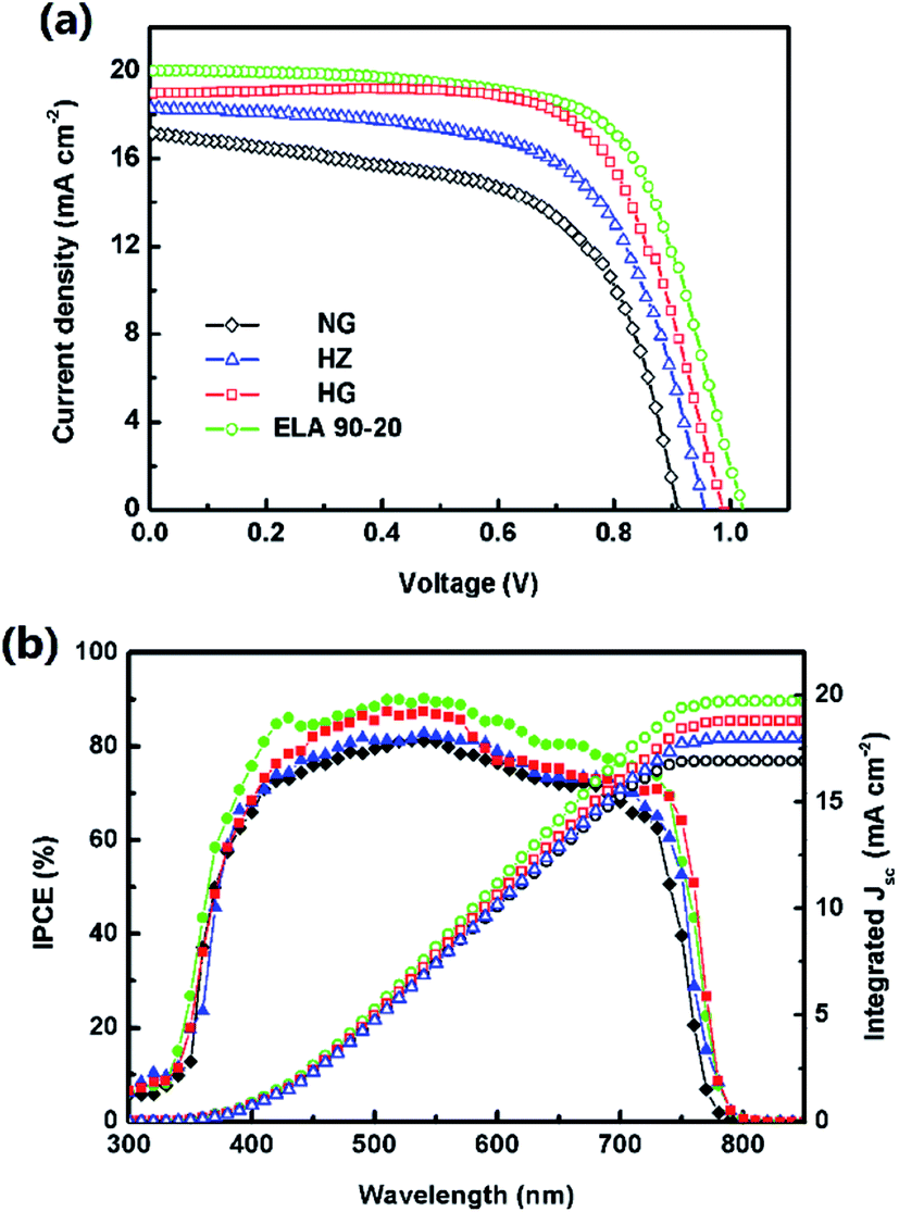 | ||
| Fig. 6 (a) J–V curves and (b) IPCE spectra and integrated photocurrent density of the PHJ-PSC based on ZnO (blue, triangle), NG (black, diamond), HG (red, square), and ELA 90-20 (green, circle). | ||
| ETL | Voc (V) | Jsc (mA cm−2) | FF (%) | PCE (%) |
|---|---|---|---|---|
| HZ | 0.95 ± 0.02 | 18.29 ± 0.31 | 63.8 ± 0.5 | 11.09 ± 0.24 |
| NG | 0.91 ± 0.02 | 17.18 ± 0.25 | 59.7 ± 0.3 | 9.33 ± 0.20 |
| HG | 0.99 ± 0.02 | 18.95 ± 0.33 | 69.1 ± 0.6 | 12.96 ± 0.31 |
| ELA 90-20 | 1.02 ± 0.02 | 20.01 ± 0.27 | 67.0 ± 0.4 | 13.68 ± 0.25 |
Charge transport between layers also contributes to the photoelectric performance of the device, i.e. when the photo electrons are generated, they should be transferred efficiently to the ETL. Herein, the charge extraction capacity of the ETL was evaluated by comparing the steady-state photoluminescence (PL) quenching behaviour between the perovskite layer and ETL. Fig. 7(a) contains the PL spectra of glass substrate/ETL/MAPbI3 structure (ETL = NG, HG, and ELA 90-20). All the curves show high intensity peaks at ca. 770 nm, which is related with the emission of the films after excitation at a wavelength of 473 nm. The PL density of the MAPbI3 film on a glass is the highest, with the other samples showing various degrees of quenching.48 When the excited electrons relax to the ground state, the energy is released mainly by photoluminescence and energy transfer and, when there is no ETL, most of the energy is released by photoluminescence, hence the strongest peak is observed for the glass substrate/MAPbI3 system. The ETLs effectively extract the excited charges, share the released energy by energy transfer, leading to the weaker photoluminescence intensity.49 Among the GZO samples, the PL density of ELA 90-20 is lower than the NG and HG ETLs, which implies the electrons can be transferred to the ETL more efficient to the ELA 90-20 film, and can be ascribed to its lower resistivity.
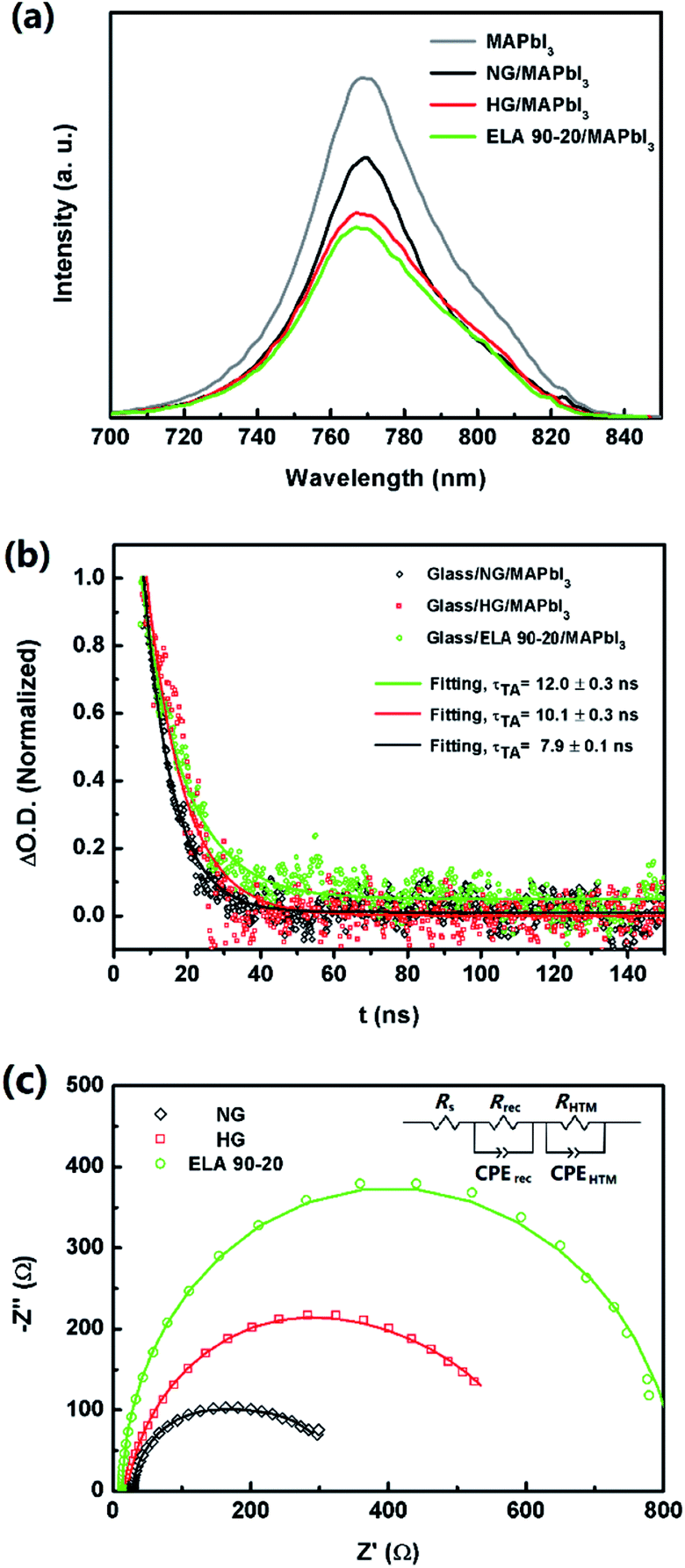 | ||
| Fig. 7 (a) PL spectra of glass substrate/ETL/MAPbI3 (ETL = NG, HG, ETL 90-20, or none) samples. (b) Transient absorption decay of glass substrate/ETL/MAPbI3 (ETL = NG, HG, and ETL 90-20) samples. (c) Nyquist plots of the PHJ-PSCs based on NG, HG, and ELA 90-20. The inset is the equivalent circuit of the cell. | ||
Transient absorption spectra (TAS) were employed to probe the dynamics of these carriers in further detail. When a laser with a wavelength of 440 nm irradiates on the perovskite layer for several nanoseconds, the electrons are excited and the photoluminescence signals are probed at 770 nm. It can be seen from Fig. 7(b) that all the samples show a transient absorption decay on the nanosecond timescale, which reflects the behaviour between perovskite films and ETLs of both charge injection and charge recombination. The charge recombination process plays the leading role since the time of electron injection from the perovskite layer to the ETLs is negligible compared with the recombination process.50,51 The recombination lifetime (τ) can be obtained from the curves by single exponential data fitting, and τ for the glass substrate/ETLs/MAPbI3 (ETL = NG, HG, and ELA 90-20) samples are 7.9 ± 0.1, 10.1 ± 0.3, and 12.0 ± 0.3 ns, respectively, which indicates the recombination process of charge existing in ELA 90-20 and MAPbI3 is longer than with the NG and HG layers. This agrees well with the order of the resistivity of the GZO films (see above). Thus, owing to the lower resistivity and also the larger bandgap of the ELA 90-20 ETL, the velocity at which photogenerated electrons is injected into the conduction band of the GZO films is enhanced, which avoids charge accumulation, and thus prevents charge recombination, leading to the improvement in Voc.52
We further investigated the recombination behaviour at the interface of the perovskite layer and ETLs through EIS measurements; the representative Nyquist plots of are shown in Fig. 7(c) and the data were fitted using Z-view software (the corresponding equivalent circuit is depicted in the inset of Fig. 7(c)). Rs is the series resistance of the circuit. RHTL, in parallel with HTL capacitance, CPEHTL, is involved with the semi-arc at high frequency, representing the resistance of the hole diffusing the HTL. Rrec, in parallel with a chemical capacitance, CPErec, is related to the semi-arc at low frequency, representing the resistance of the recombination at the interface between perovskite layer and ETL. In our measurements due to the recurring phenomenon, only the semi arc of each plot at low frequency could be observed.53,54 The Rs value seems to have no obvious difference. However, among the GZO fabricated PHJ-PSCs, the diameter of the semi arc of ELA 90-20 is larger than NG and HG, which means the Rrec of the PHJ-PSCs increase from NG to ELA 90-20, this is in agreement with the TAS measurement results, which, from another aspect, certify the charge recombination process between GZO and perovskite films can be depressed after ELA treatments.
The thermal stability of the MAPbI3 film on the ELA 90-20 ETL was compared with that on TiO2 as well as HZ films. Previously, it has been shown that MAPbI3 films are easily decomposed by surface hydroxyl groups and/or residual acetate ligands on ETL surfaces.55 It can be seen from Fig. 8 that at 70 or 100 °C, the MAPbI3 film on the HZ film starts to change from black to yellow after 10 min and turns completely yellow after 1 h, whereas the perovskite films on TiO2 and ELA 90-20 remain largely unchanged. The higher thermal stability of MAPbI3 on ELA 90-20 may be due to elimination of the surface hydroxyl groups and residual organic ligands after ELA treatment.
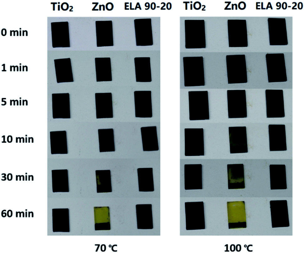 | ||
| Fig. 8 Photographs of MAPbI3 films deposited on different samples (TiO2, HZ and ELA 90-20 films) and heated to either 70 °C or 100 °C for the indicated time. | ||
Conclusions
A XeCl excimer laser with a wavelength of 308 nm was successfully applied to crystallize GZO films. Following optimization of the fluence and pulse counts, the resistivity was reduced by 4 orders of magnitude with an increase in the transmittance. According to the simulations, the surface temperature of the films irradiated at 90 mJ cm−2 approaches that of the melting point while the substrate remains close to room temperature. The PHJ-PSCs fabricated with the ELA 90-20 treated GZO ETL has a higher PCE of 13.68% with improved Voc (1.02 V) and Jsc (20.01 mA cm−2) compared with the cells based on heat treated GZO ETLs. From a comparison of the PHJ-PSCs employing the different GZO films, several advantages of ELA treated ETLs are apparent. First, high-temperatures are avoided which is beneficial in the fabrication of flexible devices. Second, the optimized ELA GZO films exhibit higher transmittance and conductivity, which improves light absorption and charge transport properties, and reduces charge recombination, leading to enhanced Jsc and Voc values. Third, the ELA treatment enhances the thermal stability of the MAPbI3 film.The ELA techniques could be extended to the crystallization of other electron and hole transport layers, such as TiO2, ZnO, SnO2, NiO, etc., to afford high quality ETLs at room temperature with universal applications in PSCs.
Conflicts of interest
There are no conflicts to declare.Acknowledgements
This work was supported by the National Natural Science Foundation of China (11674324 and 11604339), Key laboratory of Photovoltaic and Energy Conservation Materials, Anhui Provincial Key laboratory of Photonics Devices and Materials, and Key laboratory of Functional Crystals and Laser Technology, Chinese Academy of Sciences. We thank the EPFL and Swiss National Science Foundation for financial support.Notes and references
- S. Kazim, M. K. Nazeeruddin, M. Grätzel and S. Ahmad, Angew. Chem., Int. Ed., 2014, 53, 2812 CrossRef PubMed.
- J.-H. Im, C.-R. Lee, J.-W. Lee, S.-W. Park and N.-G. Park, Nanoscale, 2011, 3, 4088 RSC.
- C. C. Stoumpos, C. D. Malliakas and M. G. Kanatzidis, Inorg. Chem., 2013, 52, 9019 CrossRef PubMed.
- S. Y. Sun, T. Salim, N. Mathews, M. Duchamp, C. Boothroyd, G. C. Xing, T. C. Sum and Y. M. Lam, Energy Environ. Sci., 2014, 7, 399 Search PubMed.
- G. Xing, N. Mathews, S. Sun, S. S. Lim, Y. M. Lam, M. Grätzel, S. Mhaisalkar and T. C. Sum, Science, 2013, 342, 344 CrossRef PubMed.
- J. Burschka, N. Pellet, S.-J. Moon, R. Humphry-Baker, P. Gao, M. K. Nazeeruddin and M. Grätzel, Nature, 2013, 499, 316 CrossRef PubMed.
- N. J. Jeon, J. H. Noh, Y. C. Kim, W. S. Yang, S. Ryu and S. I. I. Seok, Nat. Mater., 2014, 13, 897 CrossRef PubMed.
- A. Kojima, K. Teshima, Y. Shirai and T. Miyasaka, J. Am. Chem. Soc., 2009, 131, 6050 CrossRef PubMed.
- NREL, Research Cell Efficiency Records, http://www.nrel.gov/ncpv/images/efficiency_chart.jpg, accessed 08 April, 2018.
- N. Ahn, D.-Y. Son, I.-H. Jang, S. M. Kang, M. Choi and N.-G. Park, J. Am. Chem. Soc., 2015, 137, 8696 CrossRef PubMed.
- H. F. Liu, Z. R. Huang, S. Y. Wei, L. L. Zheng, L. X. Xiao and Q. H. Gong, Nanoscale, 2016, 8, 28494 Search PubMed.
- K. Mahmood, S. Sarwarb and M. Mehran, RSC Adv., 2017, 7, 17044 RSC.
- H. Kim, K.-G. Lima and T.-W. Lee, Energy Environ. Sci., 2016, 9, 12 Search PubMed.
- S. D. Sung, D. P. Ojha, J. S. You, J. Lee, J. Kim and W. I. Lee, Nanoscale, 2015, 7, 8898 RSC.
- W. H. Chen, Q. Luo, X. S. Deng, J. F. Zheng, C. X. Zhang, X. H. Chen and S. M. Huang, RSC Adv., 2017, 7, 54068 RSC.
- K. Wojciechowski, M. Saliba, T. Leijtens, A. Abate and H. J. Snaith, Energy Environ. Sci., 2014, 7, 1142 Search PubMed.
- K. Ghosh, P. Busi, S. Das, J. S. Rathore and A. Laha, Mater. Res. Bull., 2018, 97, 300 CrossRef.
- M. Trifunovic, P. M. Sberna, T. Shimoda and R. Ishihara, Thin Solid Films, 2017, 638, 73 CrossRef.
- D. Y. Liu and T. L. Kelly, Nat. Photonics, 2014, 8, 133 CrossRef.
- D. Cheon, M. Son, M.-H. Ham and W. Lee, RSC Adv., 2016, 6, 103864 RSC.
- P. Sharma, R. Singh, V. Awasthi, S. K. Pandey, V. Garg and S. Mukherjee, RSC Adv., 2015, 5, 85523 RSC.
- H. Q. Le, S. K. Lim, G. K. L. Goh and W. Liu, Appl. Phys. B, 2010, 100, 705 CrossRef.
- P. Kumar, V. Sharma, A. Sarwa, A. Kumar, Surbhi, R. Goyal, K. Sachdev, S. Annapoorni, K. Asokan and D. Kanjilal, RSC Adv., 2016, 6, 89242 RSC.
- Q. Cheng, M. K. Benipal, Q. L. Liu, X. Y. Wang, P. A. Crozier, C. K. Chan and R. J. Nemanich, ACS Appl. Mater. Interfaces, 2017, 9, 16138 Search PubMed.
- J. P. Bermundo, Y. Ishikawa, M. N. Fuji, T. Nonake, R. Ishihara, H. Ikenoue and Y. Uraoka, J. Phys. D: Appl. Phys., 2016, 49, 035102 CrossRef.
- M. Hsu, N. V. Thang, C. Wang and J. Leu, Thin Solid Films, 2012, 520, 3593 CrossRef.
- E. V. Johnson, P. Prod’homme, C. Boniface, K. Huet, T. Emeraud and P. R. Cabarrocas, Sol. Energy Mater. Sol. Cells, 2011, 95, 2823 CrossRef.
- W. M. Tsang, F. L. Wong, M. K. Fung, J. C. Chang, C. S. Lee and S. T. Lee, Thin Solid Films, 2008, 517, 891 CrossRef.
- T. Shimogaki, T. Ofuji, N. Tetsuyama, H. Kawahara, M. Higashihata, H. Ikenoue, D. Nakamura and T. Okada, Proc. SPIE, 2014, 89870G Search PubMed.
- H. Kim, K. G. Lim and T. W. Lee, Energy Environ. Sci., 2016, 9, 12 Search PubMed.
- S. Q. Chen, M. E. A. Warwick and R. Binions, Sol. Energy Mater. Sol. Cells, 2015, 137, 202 CrossRef.
- S. M. Wang, W. W. Dong, X. D. Fang, Q. L. Zhang, S. Zhou, Z. H. Deng, R. H. Tao, J. Z. Shao, R. Xia, C. Song, L. H. Hu and J. Zhu, Nanoscale, 2016, 8, 6600 RSC.
- X. Q. Pan, Y. Shuai, C. Wu, W. Luo, X. Sun, Y. Yuan, S. Zhou, X. Ou and W. Zhang, Appl. Surf. Sci., 2016, 389, 1104 CrossRef.
- A. Bhaumik, J. Appl. Phys., 2017, 121, 125303 CrossRef.
- Z. W. Qiu, S. Yuan, H. B. Gong, H. L. Zhang, X. F. Qiu, T. Luo and B. Q. Cao, J. Am. Ceram. Soc., 2017, 100, 176 CrossRef.
- L. Ding, S. Nicolay, J. Steinhauser, U. Kroll and C. Ballif, Adv. Funct. Mater., 2013, 23, 5177 CrossRef.
- J. K. Sheu, K. W. Shu, M. L. Lee, C. J. Tun and G. C. Chi, J. Electrochem. Soc., 2007, 154, H521 CrossRef.
- Z. W. Qiu, H. B. Gong, G. H. J. Zheng, S. Yuan, H. L. Zhang, X. M. Zhu, H. P. Zhou and B. Q. Cao, J. Mater. Chem. C, 2017, 5, 7084 RSC.
- T. S. Moss, Proc. Phys. Soc., London, Sect. B, 1954, 67, 775 CrossRef.
- E. Burstein, Phys. Rev., 1954, 93, 632 CrossRef.
- S. Cho, S. H. Jung and K. H. Lee, J. Phys. Chem. C, 2008, 112, 12769 Search PubMed.
- X. Yu, J. Ma, F. Ji, Y. Wang, X. Zhang, C. Cheng and H. Ma, Appl. Surf. Sci., 2005, 239, 222 CrossRef.
- C. Y. Yen, S. R. Jian, G. J. Chen, C. M. Lin, H. Y. Lee, W. C. Ke, Y. Y. Liao, P. F. Yang, Y. S. Lai, J. S. C. Jang and J. Y. Juang, Appl. Surf. Sci., 2011, 257, 7900 CrossRef.
- Z. B. Fang, Z. J. Yan, Y. S. Tan, X. Q. Liu and Y. Y. Wang, Appl. Surf. Sci., 2005, 241, 303 CrossRef.
- Q. Nian, M. Callahan, M. Saei, D. Look, H. Efstathiadis, J. Bailey and G. J. Cheng, Sci. Rep., 2015, 5, 15517 CrossRef PubMed.
- P. X. Gao, C. S. Lao, Y. Ding and Z. L. Wang, Adv. Funct. Mater., 2006, 16, 53 CrossRef.
- Y. G. Rong, S. Venkatesan, R. Guo, Y. N. Wang, J. M. Bao, W. Z. Li, Z. Y. Fan and Y. Yao, Nanoscale, 2016, 8, 12892 RSC.
- N. Mondal and A. Samanta, Nanoscale, 2017, 9, 1878 RSC.
- W. D. Xu, J. A. McLeod, Y. G. Yang, Y. M. Wang, Z. W. Wu, S. Bai, Z. C. Yuan, T. Song, Y. S. Wang, J. J. Si, R. B. Wang, X. Y. Gao, X. P. Zhang, L. J. Liu and B. Q. Sun, ACS Appl. Mater. Interfaces, 2016, 8, 23181 Search PubMed.
- L. Z. Zhu, J. J. Ye, X. H. Zhang, H. Y. Zheng, G. Z. Liu, X. Pan and S. Y. Dai, J. Mater. Chem. A, 2017, 5, 3675 Search PubMed.
- A. M. A. Leguy, P. Azarhoosh, M. I. Alonso, M. Campoy-Quiles, O. J. Weber, J. Z. Yao, D. Bryant, M. T. Weller, J. Nelson and A. Walsh, Nanoscale, 2016, 8, 6317 RSC.
- G. S. Han, Y. H. Song, Y. U. Jin, J.-W. Lee, N.-G. Park, B. K. Kang, J.-K. Lee, I. S. Cho, D. H. Yoon and H. S. Jung, ACS Appl. Mater. Interfaces, 2015, 7, 23521 Search PubMed.
- J. A. Christians, R. C. M. Fung and P. V. Kamat, J. Am. Chem. Soc., 2014, 136, 758 CrossRef PubMed.
- K. Cao, H. Li, S. S. Liu, J. Cui, Y. Shen and M. K. Wang, Nanoscale, 2016, 8, 8839 RSC.
- J. L. Yang, B. D. Siempelkamp, E. Mosconi, F. D. Angelis and T. L. Kelly, Chem. Mater., 2015, 27, 4229 CrossRef.
Footnote |
| † Electronic supplementary information (ESI) available. See DOI: 10.1039/c8ra03119c |
| This journal is © The Royal Society of Chemistry 2018 |