
 Open Access Article
 This Open Access Article is licensed under a Creative Commons Attribution-Non Commercial 3.0 Unported Licence
Atomic-scale investigation of MgO growth on fused quartz using angle-dependent NEXAFS measurements†
Jitendra Pal Singh *a,
So Hee Kima,
Sung Ok Wona,
Ik-Jae Leeb and
Keun Hwa Chae*a
*a,
So Hee Kima,
Sung Ok Wona,
Ik-Jae Leeb and
Keun Hwa Chae*a
aAdvanced Analysis Center, Korea Institute of Science and Technology, Seoul 02792, Republic of Korea. E-mail: jitendra_singh2029@rediffmail.com; khchae@kist.re.kr
bBeamline Division, Pohang Accelerator Lab, Pohang 37673, Republic of Korea
First published on 5th September 2018
Abstract
The phenomena related to thin film growth have always been interesting to the scientific community. Experiments related to these phenomena not only provide an understanding but also suggest a path for the controlled growth of these films. For the present work, MgO thin film growth on fused quartz was investigated using angle-dependent near-edge X-ray absorption fine structure (NEXAFS) measurements. To understand the growth of MgO, sputtering was allowed for 5, 10, 25, 36, 49, 81, 144, 256, and 400 min in a vacuum better than 5.0 × 10⁻⁷ torr. NEXAFS measurements revealed the evolution of MgO at the surface of fused quartz for sputtering durations of 144, 256, and 400 min. Below these sputtering durations, no MgO was observed. NEXAFS measurements further envisaged a systematic improvement of Mg2+ ion coordination in the MgO lattice with the sputtering duration. The onset of non-interacting molecular oxygen on the surface of the sputtered species on fused quartz was also observed for sputtering duration up to 81 min. Angle-dependent measurements exhibited the onset of an anisotropic nature of the formed chemical bonds with sputtering, which dominated for higher sputtering duration. X-ray diffraction (XRD) studies carried out for sputtering durations of 144, 256, and 400 min exhibited the presence of the rocksalt phase of MgO. Annealing at 700 °C led to the dominant local electronic structure and improved the crystallinity of MgO. Rutherford backscattering spectrometry (RBS) and cross-sectional scanning electron microscopy (SEM) revealed a layer of almost 80 nm was obtained for a sputtering duration of 400 min. Thus, these angle-dependent NEXAFS measurements along with XRD, RBS, and SEM analyses were able to give a complete account for the growth of the thin films. Moreover, information specific to the coordination of the ions, which is important in case of ultrathin films, could be obtained successfully using this technique.
Introduction
The mechanism behind thin film growth is an interesting phenomenon and has been a matter of debate for long time.1–3 Based on various approaches, mathematical models developed for the determination of film growth were illustrated by Forgerini and Marchiori (2014).4 The microstructural evolution of film growth is governed by number of different processes, such as nucleation, coalescence, competitive grain growth, and recrystallization.5 In addition to these processes, it is reported that processes like adsorption and surface reaction not only promote film growth but also influence the surface properties of thin films.6 However, understanding thin film growth still remains a topic of debate among researchers of both theoretical and experimental background. The zeal to understand thin film growth among researchers can be seen in a recent review by Sahu et al.7Haberland et al. utilized molecular dynamics simulation to understand the nature of Mo (001) surfaces by considering an energetic cluster impact model. The formation of a porous film was calculated for clusters with a low kinetic energy, while for clusters with the highest energy, a dense mirror-like film was obtained.8 Levine et al. performed grazing-incidence small-angle X-ray scattering to understand the growth of Au films.9 Kratzer et al. simulated density-functional theory (DFT) calculations for understanding molecular beam epitaxy (MBE) grown GaAs and InGaAs films at the atomic level.10 Rahman et al. proposed a kinematic Monte Carlo simulation model to understand the atomistic and morphological growth of thin films.11 A mathematical formalism was developed to describe the evolution of the intensity of ion scattering spectroscopy (ISS) against X-ray photoelectron spectroscopy (XPS) peaks when thin film is deposited on a flat substrate. This formalism permitted researchers to differentiate a layer-by-layer growth mechanism from islands and provided an approximate value of the thickness of a homogeneous layer of the deposited film. The model has been applied to study the deposition of oxide thin films of SnO and CoO on substrates of other oxide materials like MgO and SiO2. These studies reflect that the growth of thin films not only depends on the growth parameters but also on the method of deposition along with the composition of the thin film.12 Apart from the growth of inorganic thin films, complexation arises when organic thin films are grown.13–15 The growth mechanism becomes even more interesting in the case of bilayers and heterostructures, where the growth of a preceding layer is highly crucial.16–18 In addition to this, the interaction among ions/atoms at an interface affects the behavior of heterostructures and sometimes gives rise to completely different phenomena.19,20 Thus, this study intended to gain an understanding of the growth of thin films by a technique that could not only give element-specific details but that could also provide information about the interaction with neighboring atoms/ions. These requirements leave us on to near-edge X-ray absorption fine structure (NEXAFS) investigations as these provide valence state and site-specific information about atoms/ions in the lattice.21,22 These measurements also give information about the hybridization taking place among various atoms/ions, which is a better process to understand the interaction among atoms during the film/crystal growth.23,24 During growth, the formation of chemical bonds in different directions occurs, which leads to the existence of anisotropic chemical bonds. In the presence of anisotropy of the chemical bonds, the contribution of individual absorption transitions is different at different angles. This leads to a redistribution of the intensity between the spectrum details. Further, evolution of this interaction in different directions could be successfully depicted using angle-dependent NEXAFS spectroscopy for organic molecules,25 oriented ZnO nanostructures,26 and Pr0.67Sr0.33MnO3 films.27 Thus, NEXAFS investigations were extended to angle-dependent measurements in the present study.28–30
In recent years, MgO has attracted more interest due to its unusual magnetism31–34 and optical behavior.35–37 This material is also known for phenomena like spin-dependent electron reflection,38 multilevel switching characteristics,39 and broad-band laser emission.40 The catalytic applications of this material have attracted a lot of research in different disciplines in recent years.41–44 Thus, the importance of MgO in several applications and the emergence of novel phenomena makes it a preferred choice for this investigation. Moreover, the NEAXFS spectra of the MgO system are sensitive to any external treatment45–48 and are able to give layer-by-layer information on thin films.49,50 Since the film formation during any deposition technique involves an atom-by-atom and layer-by-layer interaction, these measurements are able to give information about the growth more precisely. Thus, the importance of MgO and its sensitivity toward NEXAFS motivated us to select MgO for understanding the growth phenomenon. As discussed earlier, the nature of the substrate and the deposition methods play important roles in determining the growth; hence, the growth of MgO on fused quartz (amorphous SiO2) was considered as a better choice for the present investigation. The key benefit of considering an amorphous substrate was prevention of the preferred growth that dominates in case of a crystalline substrate.51 It is considered that the growth of MgO on this substrate was only affected by interaction among the constituent atoms.
Though a number of methods, such as pulsed laser deposition,52 molecular beam epitaxy,53 atomic layer deposition,54 and e-beam evaporation methods55 are being developed for depositing MgO thin films, the radio-frequency (rf) sputtering method is considered the most suitable for an insulating oxide like MgO.56–58 Thus, the present work was motivated to investigate the growth of MgO on a fused quartz substrate using the rf-sputtering method together with angle-dependent NEXAFS measurements.
Experimental
Growth procedure for sputtering
In order to understand the nature of MgO film growth systematically, MgO-sputtering target (99.99%) procured from Alfa Aesar was used for sputtering. The MgO target was sputtered on fused quartz substrates using the rf-sputtering method for various deposition durations of 5, 10, 15, 25, 36, 49, 64, 81, 144, 256, and 400 min.58 The base pressure for sputtering was 5.0 × 10⁻⁷ torr. During deposition, the Ar pressure was maintained at 4.0 mTorr. The target to substrate distance was kept at 5 cm for the sputtering of MgO on fused quartz (Fig. 1: upper panel). The substrate temperature was kept at room temperature (300 K). The rf power was maintained at 40 W for all sputtering durations.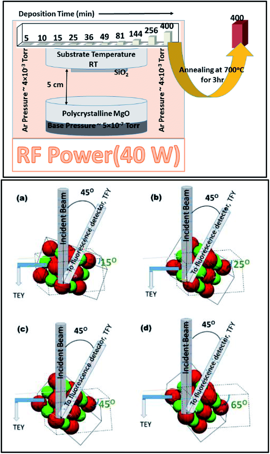 | ||
| Fig. 1 Process of MgO sputtering and annealing on an amorphous fused quartz substrate for sputtering durations of 5, 10, 15, 25, 36, 49, 81, 144, 256, and 400 min (upper panel); schematic of TEY and TFY measurements at an angle of: (a) 15°, (b) 25°, (c) 45°, and (d) 65° from beam incidence (lower panel). Gray and white pillars show the direction of the incident and outgoing X-ray beam. The outgoing beam was detected by a fluorescence detector situated at 45° from beam direction. Red and green spheres represent Mg2+ and O2− ions, respectively. | ||
In order to investigate the crystallinity improvement associated with annealing, the sputtered species having sputtering duration of 400 min were further annealed at 700 °C for 3 h (Fig. 1: upper panel).
Characterization
NEXAFS measurements for all the sputtering durations were performed at the X-ray 10D XAS KIST (Korea Institute of Science and Technology) beamline of the Pohang Accelerator Laboratory (PAL), Pohang, South Korea. This beamline operates at 3.0 GeV energy with a maximum storage current of 360 mA. All the spectra were collected at room temperature in a vacuum ∼1.5 × 10⁻⁸ torr. Gratings with 1400 (G3) and 1800 grooves per mm (G4) with an entrance and exit slit size of 100 μm × 100 μm were utilized for collecting the spectra at the O- and Mg K-edges. The energy resolution was 0.6 and 1 eV for gratings G3 and G4, respectively.59,60To obtain information on the bulk and surface characteristics of the sputtered species on the fused quartz substrate, NEXAFS measurements were simultaneously measured in bulk sensitive, total fluorescence yield (TFY) mode along with surface-sensitive, total electron yield (TEY) modes (Fig. S1†). A voltage of 1.75 kV was applied to the micro-channel plate (MCP) for measuring the NEXAFS spectra in the TFY mode. For these measurements, a fluorescence detector was placed at fixed angle of 45° from the direction of the beam axis.60 Typically, the probing depth of X-ray in the TEY mode is 5–10 nm,61 which increases to almost one order of magnitude in the TFY mode.62,63 Asakura et al. mentioned that soft X-rays in this mode can probe the electronic structure as deep as 100 nm in the case of an oxide thin film.63
To further investigate the evolution of growth in different directions, angle-dependent NEXAFS measurements were performed in both TEY and TFY modes. The sample holder was rotated at different angles with respect to the direction of the beam incidence. These angles were 15°, 25°, 45°, and 65° from the direction of beam incidence (Fig. 1: lower panel). The active area of the fluorescence detector was 40 mm in diameter to enable detection of photons in all measuring directions. The incident photon flux (Io) was measured by inserting a gold (Au) mesh in the path of the X-ray beam. All the spectra were background subtracted and normalized with respect to the incident photon flux (Io).59 A schematic of the angle dependence is shown in Fig. 1 (lower panel). The schematic clearly shows that the Mg–O interaction could be clearly investigated in different directions while measuring the NEXAFS spectra at 15°, 25°, 45°, and 65°.
X-ray diffraction (XRD) patterns at various sputtering durations were measured using a D/MAX2500 (RIGAKU, Japan) X-ray diffractometer at Cu-Kα (λ = 1.54148 Å) radiation in order to throw light on the crystallinity of the sputtered species. The step size and scan rate were 0.02° and 0.1° s−1 for measuring the XRD patterns.
Rutherford backscattering spectrometry (RBS) for sputtering duration of 400 min was carried out using an NEC Pelletron 6SDH-2 Accelerator to get information on the sputtered film thickness. The depth resolution of the RBS spectrometer was 10 nm. RBS simulation was performed using the RUMP program.64 To further corroborate the results obtained from the RBS spectrum, cross-sectional scanning electron microscopy (SEM) measurements for a sputtering duration of 400 min and its annealed counterpart were performed using an Hitachi (S-4200) field emission scanning electron microscope. To determine thickness, the thickness across the sputtered species was measured at several points using ImageJ software. A histogram was plotted between the thickness and number of counts. The histogram was fitted using a Gaussian function to find the thickness.65
Results
In order to understand the nature of growth at the surface and deep in the sputtered species on fused quartz substrate, the local electronic structure for different sputtering durations is discussed as a function of the sputtering duration and annealing.Local electronic structure for different sputtering durations
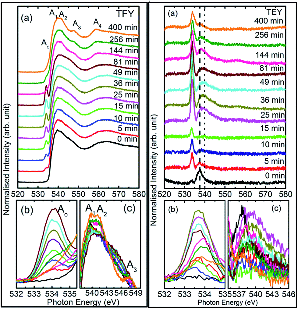 | ||
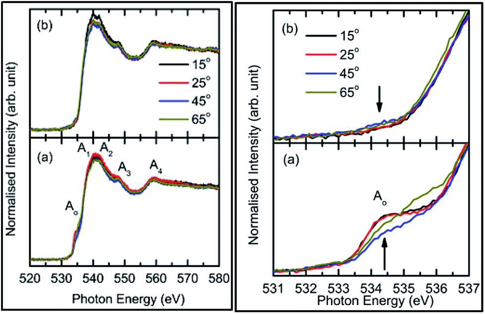
| Fig. 2 Left panel shows (a) TFY O K-edge spectra of MgO sputtered on fused quartz substrate, (b) pre-edge spectral feature, Ao, and (c) A1, A2, A3 spectral feature regions right panel shows the corresponding measurements in TEY mode. Numerals in both panels represent the sputtering duration. | ||
To understand this, we focus our attention on the spectral features A1, A2, and A3 in the range 538–549 eV for all sputtering durations, as shown in Fig. 2c (left panel). The spectra in this range exhibit different shape for sputtering durations of 144 min and onwards compared to previous sputtering durations. The signatures of the A1, A2, and A3 spectral features can be clearly seen for sputtering durations of 144, 256, and 400 min. This indicates possible hybridization among the Mg(1s)–O(2p) hybridized states, which initiate the growth of MgO formation. Thus, the decrease of pre-edge intensity after certain deposition times is due to the interaction of the sputtered ions themselves to fasten the process of MgO formation, thus inhibiting the ions contributing toward the pre-edge spectral feature.
Thus, the quartz surface will be modified with the increase in sputtering duration as sputtering species are populating it; hence, the surface-sensitive TEY mode NEXAFS spectra are shown in Fig. 2a (right panel) to highlight this. At all sputtering durations, the spectral features are markedly different compared to the TFY counterpart (Fig. 2a: left panel). The different nature is due to the highly insulating nature of quartz. However, these spectra also reflect the modifications of the intensity of the spectral feature in the pre-edge region with the increase in sputtering duration (Fig. 2b: right panel). Moreover, the intensity of the pre-edge spectral feature is at a maximum for a sputtering duration for 81 min. The intensity of the pre-edge spectral feature later decreases for a sputtering duration of 144 min and onwards. This behavior is analogous to the intensity variation of the corresponding TFY counterpart (Fig. 2b: left panel). Thus, these investigations also reflect surface modification during the sputtering process. Even though the post region of the TEY-mode NEXAFS spectra do not exhibit an evolution of the spectral features A1, A2, A3, and A4 after a sputtering duration of 144 min (Fig. 2a: right panel), as in the case of the TFY mode (Fig. 2a: left panel); the, broad region in 538–544 eV exhibits modifications with the sputtering duration. The maxima of this region exhibits a shift toward a higher energy value with increasing the sputtering duration (Fig. 2c: right panel). These observations again infer quartz surface modifications with the increase in sputtering duration. However, the spectral features representing the MgO phase are not distinguishable as in the TFY-mode NEXAFS spectra of these films.
Consequently, O K-edge spectra for certain sputtering durations were performed in TFY modes at different angles in order to get in-depth insights of the sputtered species. Fig. 3 shows the angle-dependent TFY-mode O K-edge NEXAFS spectra at sputtering durations of: (a) 0 min, (b) 5 min, (c) 25 min, (d) 81 min, (e) 144 min, and (f) 256 min. A visual inspection shows that these spectra concur with those reported in Fig. 2. This indicates the reproducibility of both the measurements as well as the growth of film with the sputtering duration. A visual inspection of these spectra measured for different sputtering durations envisages that the shape of these spectra remains the same irrespective of the angle of measurements. At a sputtering duration of 0 min, the O K-edge spectra at 15°, 25°, 45°, and 65° exhibit almost a similar shape (Fig. 3a) to that shown in Fig. 2a (left panel). These spectra at all measuring angles are characterized by two broad features centered at 539.5 ± 0.1 eV and 562.5 ± 0.1 eV (Fig. 3a). In addition to these prominent features, a shoulder-like feature (indicated by arrow) is also observed at 543.2 ± 0.1 eV. Moreover, the pre-edge region shown in the inset shows the absence of any spectral feature, irrespective of the incident angle (Fig. 3a: inset). The shape of the O K-edge spectra at different angles is very much analogous to the spectrum of SiO2 reported by Khyzhun et al.72 As the sputtering duration is increased to 5 min, prominent broad spectral features at 539.5 ± 0.1 eV and 562.5 ± 0.1 eV exist with almost a negligible change of shape (Fig. 3b). In addition to this, the shoulder-like feature is also not influenced by such a small sputtering duration increase (Fig. 3b). Apart from this, a small spectral feature centered at 534.5 ± 0.1 eV evolves in the pre-edge region of the O K-edge spectra. The pre-edge region shown as the inset of Fig. 3b indicates that this spectral feature occurs in the O K-edge spectra at all angles. At a sputtering duration of 25 min, the intensity of the pre-edge increases, revealing the increase of sputtered ions on the fused quartz surface (Fig. 3c).
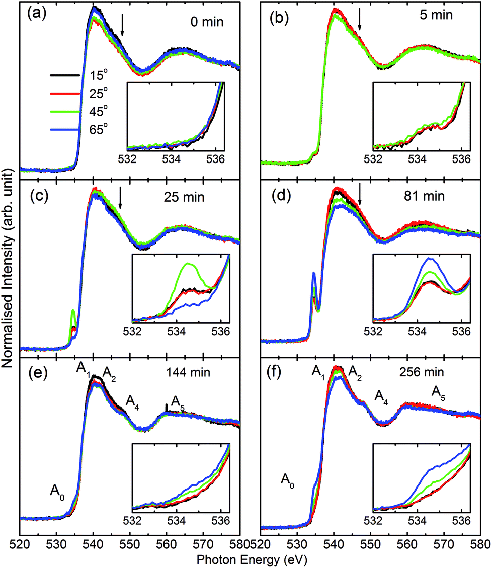 | ||
| Fig. 3 TFY O K-edge spectra of MgO sputtered on quartz substrate at different angles (15°, 25°, 45°, and 65°) for deposition durations of: (a) 0 min, (b) 5 min, (c) 25 min, (d) 81 min, (e) 144 min, and (f) 256 min. The spectral features Ao, A1, A2, A3, and A4 are mentioned in panels in (e) and (f). The inset of each panel shows a zoomed-in section of the pre-edge region. Arrows highlight the shoulder in these spectra. | ||
When sputtering is increased to 81 min, the intensity of the pre-edge region increases (Fig. 3d). At this sputtering duration, a systematic change with the angle is observed. Apart from a systematic change in the pre-edge region for sputtering durations of 25 and 81 min, major changes are also observed in the post-edge region of the O K-edge spectra. Though prominent broad spectral features at 539.5 ± 0.1 eV and 562.5 ± 0.1 eV appear at both these sputtering durations, the shoulder region is modified at these sputtering durations. This shoulder feature now has a broad nature. These modifications in the shoulder are reflected at all angles. This reveals that interactions among the ions are initiated to form MgO at these sputtering durations. When the sputtering duration is increased to 144 min, the pre-edge region spectral feature Ao intensity is reduced (Fig. 3e). This effect is observed at all angles. Moreover, the spectral features A1, A2, A3, and A4 centered at 534.1 ± 0.1, 539.7 ± 0.1, 541.8 ± 0.1, 547.8 ± 0.1, and 558.6 ± 0.1 eV can also be observed.73,74 This reveals that the interaction among Mg2+ and O2− occur at a sputtering duration of 144 min to form a MgO unit cell. These spectral features are more visible at a sputtering duration of 256 min when the NEXAFS spectra are measured at 15°, 25°, 45°, and 60° (Fig. 3f). This indicates that the formation of MgO occurs at this sputtering duration. As discussed in this section, the O K-edge spectra give systematic information on the growth of MgO on fused quartz with the sputtering duration. Since the TFY-mode O K-edge spectra at 15°, 25°, 45°, and 60° for different durations have a dominant contribution from quartz rather than MgO, quantitative information on the hybridization during growth would be indispensable. Also, systematic growth investigations of Mg ions cannot be reflected by the O K-edge spectra. Thus, information on thin film growth was obtained by measuring the Mg K-edge spectra in both TEY and TFY modes for different sputtering durations, which is discussed in the next section.
 | ||
| Fig. 4 (a) TFY- and (b) TEY-mode Mg K-edge NEXAFS spectra of sputtered MgO for different durations. In (b), the positions of the main spectral features B, B1, and B2 are also shown for the measured spectra in the TFY mode (left panel) and TEY mode (right panel). Inset (b) (right panel), de-convolution of the spectral features. | ||
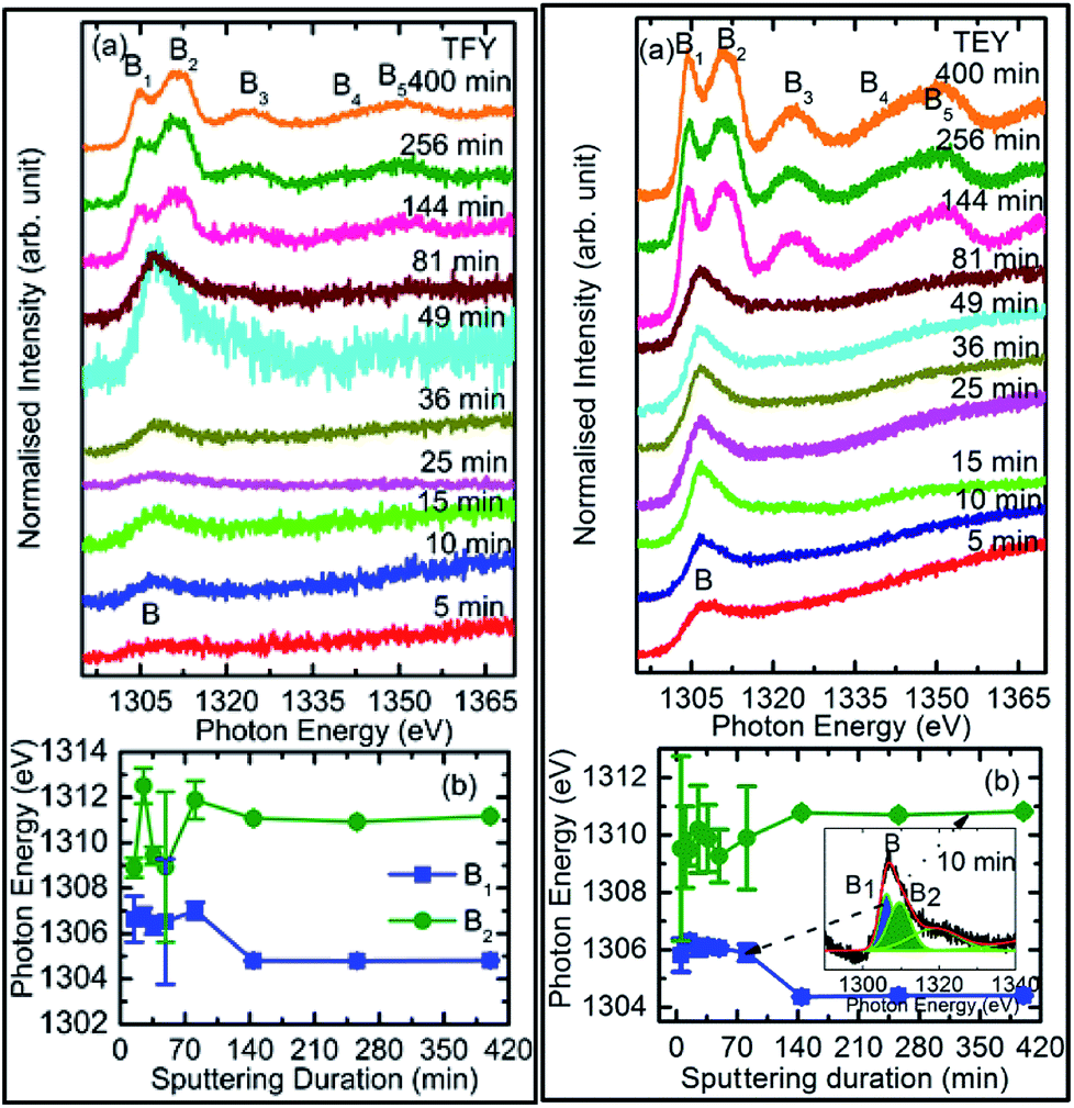
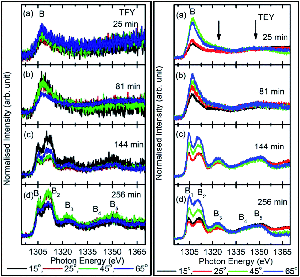
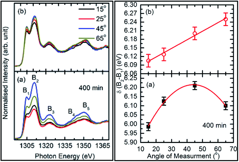
To check the reproducibility of these measurements, NEXAFS spectra were repeated in the energy range 1295–1330 eV (Fig. S3†). It is clear from these measurements that the trend of these spectra with the different sputtering durations is almost the same. The TFY-mode NEXAFS spectra exhibit the presence of a spectral feature, B, for a sputtering duration of 5 min. With an increase in sputtering duration, the intensity of this spectral feature increases up to a sputtering duration of 81 min. This spectral feature is generally present in the Mg K-edge spectra of Mg nanoparticles (Fig. 4a: left panel). Thus, this spectral feature shows the presence of Mg2+ ions on the substrate. This indicates that Mg2+ ions are far from attaining the coordination characteristics to MgO since, there is no spectral feature showing the interaction of Mg2+ and O2−, and hence there is weak interaction among these ions up to sputtering duration of 81 min. When the sputtering duration is increased to 144 min, a drastic change occurs in the spectrum, which then exhibits spectral features B1, B2, B3, B4, and B5 centered at 1305, 1311, 1323, 1340, and 1350 eV, respectively. These spectral features also exist in the spectra measured for sputtering durations of 256 and 400 min. These spectral features are relevant with the Mg K-edge spectrum of bulk MgO. The detailed description of the origin of these spectral features is given elsewhere73,74 and these were observed for MgO thin films44,46,66 and nanoparticle by our group.36,37
The presence of only one spectral feature, B, for sputtering duration of 81 min reveals the absence of interaction specific to MgO formation among Mg2+ and O2− ions. However, the O K-edge NEXAFS spectra reveal such interaction among Mg2+ and O2− ions. Thus, a deeper understanding about the interaction of these ions was accomplished by de-convoluting the spectral feature, B, (into B1 and B2) of the Mg K-NEXAFS spectra. The positions of the de-convoluted sub-spectral features B1 and B2 for sputtering durations of 5, 10, 15, 25, 36, 49, and 81 min along with the spectral features B1 and B2 for sputtering durations of 144, 256, and 400 min are shown in Fig. 4b (left panel) and Fig. 4b (right panel) for TFY and TEY modes, respectively. This envisages that the interaction among Mg2+ and O2− ions changes systematically with the sputtering duration. Further, the positions of various spectral features at these sputtering durations were estimated from Gaussian fitting of the spectrum (Fig. S4†). The spectral feature B1 appears at 1306.63 ± 1.10, 1306.7 ± 0.38, 1306.36 ± 0.38, 1306.52 ± 2.76, 1307.01 ± 0.36, 1304.8 ± 0.03, 1304.79 ± 0.02, and 1304.81 eV for sputtering durations of 15, 25, 36, 49, 81, 144, 256, and 324 min, respectively, when the Mg K-edge spectra was measured in the TFY mode (Fig. 4b: left panel). At these sputtering durations, the spectral feature, B2, is observed at 1308.9 ± 0.43, 1312.50 ± 0.78, 1309.43 ± 0.38, 1308.93 ± 3.31, 1311.88 ± 0.83, 1311.08 ± 0.03, 1310.92 ± 0.02, and 1311.17 ± 0.02 eV. It is clear from these values that the positions of B1 and B2 values for sputtering durations of 144, 256, and 400 min are close to the values for the Mg K-edge spectrum of MgO bulk. Moreover, the differences in these spectral features (δB1B2) are close to 6.33 eV for these deposition durations (Fig. 4b: left panel).75 This reveals that the deepness of the sputtered species on the substrate can be characterized by the formation of MgO for these sputtering durations.
Analogous to the TFY NEXAFS spectra (Fig. 4a: left panel), the TEY NEXAFS spectra exhibit only one spectral feature, B, up to the sputtering duration of 81 min from 5 min (Fig. 4a: right panel). The spectral feature B1 appears at 1305.81 ± 0.58, 1306.19 ± 0.18, 1306.30 ± 0.06, 1306.07 ± 0.28, 1306.13 ± 0.12, 1306.06 ± 0.08, 1305.90 ± 0.29, 1304.36 ± 0.02, 1304.40 ± 0.02, and 1304.41 ± 0.02 eV for sputtering durations of 5, 10, 15, 25, 36, 49, 81, 144, 256, and 324 min, respectively, when the Mg K-edge spectra was measured in the TEY mode (Fig. 4b: right panel). At these sputtering durations, the spectral feature, B2, is observed at 1305.81 ± 0.58, 1306.19 ± 0.18, 1308.9 ± 0.43, 1312.50 ± 0.78, 1309.43 ± 0.38, 1308.93 ± 3.31, 1311.88 ± 0.83, 1311.08 ± 0.03, 1310.92 ± 0.02, and 1311.17 ± 0.02 eV. It is clear from these values that the positions of the B1 and B2 values for sputtering durations of 144, 256, and 400 min are close to the values for the Mg K-edge spectrum of MgO bulk. Moreover, the differences among these spectral features (δB1B2) are close to 6.34 eV for these deposition durations (Fig. 4b: right panel). These values infer the formation of a well-defined MgO unit cell for sputtering durations of 144 min, 256, and 400 min. Thus, the surface behavior for this sputtering duration is analogous to the bulk behavior. While for deposition durations of 5, 10, 15, 25, 36, 49, and 81 min, these values exhibit a deviation from that of bulk MgO, which reveals the presence of non-interacting Mg2+ and O2− ions at the surface. Thus, both types of measurements suggest that Mg2+ ions are not interacting with O2−, revealing the same kind nature of Mg2+ inside the bulk as well as at the surface. TEY NEXAFS spectra were also repeated in order to check the reproducibility of the measurements, and the results are shown in Fig. S3.† These spectra also show a similar variation of Mg K-edge spectra with sputtering duration, which again reflects the reproducibility of the observed growth behavior. Thus, the O K-edge and Mg K-edge spectra measured for several sputtering durations exhibit interesting changes, which is very interesting in order to know the growth mechanism. In order to deepen the underlying mechanism, these measurements were also performed at different angles for selected sputtering durations in both TEY and TFY modes. The TFY-mode NEXAFS measurements at 15°, 25°, 45°, and 65° for a sputtering duration of 5 min are shown in Fig. S5.† In both modes, the Mg K-edge spectra are characterized by one spectral feature, B, at all angles, as shown in Fig. 5. A similar behavior of the Mg K-edge spectrum can be observed when Mg nanoparticles are exposed to various gaseous environments47,48 Thus, presence of only one spectral feature at all angles for these sputtering durations envisages that the coordination of Mg2+ ions is not similar to that possessed by these ions in the MgO unit cell.
 | ||
| Fig. 5 TFY (left panel) and TEY (right panel) Mg K-edge NEXAFS spectra of MgO sputtered on fused quartz substrate at different angles for sputtering durations: of (a) 25 min, (b) 81 min, (c) 144 min, and (d) 256 min. Numerals represent angles of measurements. | ||
To further investigate growth, the TEY- and TFY-mode NEXAFS spectra for sputtering durations of 25, 81, 144, and 256 min at different angles are shown in Fig. 5. It is clear from a visual inspection of the TFY (Fig. 5a: left panel) and TEY (Fig. 5a: right panel) NEXAFS spectra for a sputtering duration of 25 min that the dominant spectral feature, B, occurs at different measuring angles (15°, 25°, 45°, and 65°). The shape of these spectra remains the same for different angles (Fig. 5a). A similar behavior of these spectra was observed for a sputtering duration of 81 min (Fig. 5b). In the TEY NEXAFS spectra of both sputtering durations, signatures of the spectral features B3 and B5 (shown by arrows) also can be seen clearly (Fig. 5a and b: right panels). However, the signatures of these spectral features in the TFY mode are diminished in the TFY NEXAFS spectra for these sputtering durations (Fig. 5a and b: left panels). This is due to the lower resolution of the TFY-mode measurements compared to with the TEY mode. The onset of the spectral features B3 and B5 are not distinguishable in both the TEY and TFY NEXAFS spectra for a sputtering duration of 25 min; however, the spectral feature B still appears at such a low sputtering duration (Fig. S5†). Thus, these angle-dependent investigations corroborate the results discussed in Fig. 4. For these sputtering durations, it is evident that the spectra measured at 15° and 25° coincide. At the same time, a strong angular dependence for the intensity is observed at 45° and 60°. A strong angular dependence was also revealed for a sputtering duration of 5 min (Fig. S5†).
We further focus our attention on the sputtering durations of 144 min and 256 min. The TEY (left panel) and TFY (right panel) NEXAFS spectra at different measuring angles 15°, 25°, 45°, and 65° for these sputtering durations are shown in Fig. 5c and d, the spectra shown in Fig. 5c and d exhibit the same spectral features at all angles and in both TFY and TEY modes. The spectral features are B1, B2, B3, B4, and B5 centered at 1304.5, 1311.2, 1321.2, 1339.8, and 1348.2 eV, respectively. The presence of these spectral features at all measuring angles, i.e., 15°, 25°, 45°, and 65°, indicates that Mg2+ ions exist in a proper coordination with O2− in different directions. For these sputtering durations also, the variation of intensity with angle was observed. This variation may be due to the anisotropic nature of the chemical bonds in different directions.28–30
To further elucidate the nature of the hybridization at these sputtering durations, Mg K-edge spectra were de-convoluted using Gaussian peak fitting, as shown in Fig. S4.† The energy difference between the B1 and B2 spectral features in both modes along with their intensity ratio was estimated, and the results are shown in Fig. 6.
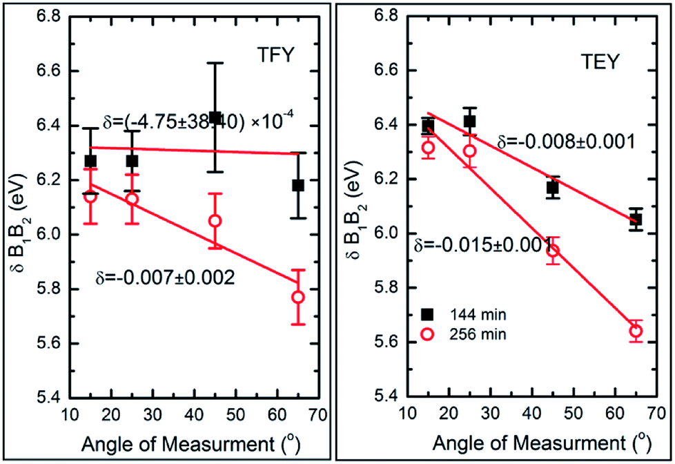 | ||
| Fig. 6 Variation of B2 and B1 differences (δB1B2) with the angles of measurements for MgO sputtering durations of 144 and 256 min in both the TFY mode (left panel) and TEY mode (right panel), where δ denotes the slope in eV per degree of the respective curve. | ||
We have not estimated δB1B2 values by de-convoluting the spectral feature B for the deposition durations of 5, 10, 15, 25, 36, 49, and 81 min-sputtered species since they do not reflect the characteristics spectral features of MgO for these durations. The energy differences of these spectral features change with the angle of measurement when estimated in both TFY (Fig. 6: left panel) and TEY modes (Fig. 6: right panel).
These values at 15°, 25°, 45°, and 65° for sputtering durations of 144 and 256 min are comparable to that of bulk MgO (Fig. 6). It is clear from this figure that these values change with the angle of measurements and that the variation can be fitted by a linear function. To obtain quantitative information on this variation, the slope (δ) of linear fit is mentioned along with the respective curve. In TFY mode, the δ value is almost negligible for a sputtering duration of 144 min; however, the δ value is significant for a sputtering duration of 256 min (Fig. 6: left panel). In this case, the slope dominates for a sputtering duration of 256 min. A similar behavior of slope was observed when the spectra were measured in TEY mode (Fig. 6: right panel). Thus, modification of the slope of δB1B2 values with measuring the angles for sputtering durations of 144 and 256 min in both t modes reflects the onset of the isotropic nature of the formation of a MgO unit cell. Table 1 shows the ratios of spectral features B1 and B2 for these sputtering durations, which are similar to those of bulk MgO.75
| Angles | B1/B2 ratio | |||
|---|---|---|---|---|
| 144 min | 256 min | |||
| TEY | TFY | TEY | TFY | |
| 15° | 0.36 | 0.26 | 0.37 | 0.29 |
| 25° | 0.35 | 0.29 | 0.34 | 0.25 |
| 45° | 0.37 | 0.22 | 0.33 | 0.21 |
| 65° | 0.39 | 0.26 | 0.33 | 0.21 |
Thus, NEXAFS measurements in both TEY and TFY modes revealed the presence of characteristic spectral features at different angles for deposition durations of 144, 256, and 400 min. The values of δB1B2 measured at 15°, 30°, 45°, and 60° were in agreement with the formation of a MgO unit cell. Thus, NEXAFS measurements were able to give information on MgO growth locally. We further extended our investigations to explore the nature of the long-range order of sputtered species for these sputtering durations. This aspect was studied using XRD measurements and is discussed in the next section.
Structure and thickness of the as-grown thin film
The XRD measurements for sputtering durations of: (a) 144 min, (b) 256 min, and (c) 400 min along with JCPDS card no. 78-0430 are shown in Fig. 7 (left panel). Sputtering durations of 144 min and 256 min did not exhibit any peak except for two major humps at 44° and 62°. The behavior of the XRD pattern for a sputtering duration of 400 min was slightly different than for its preceding durations. At this sputtering duration, a well-defined peak at 62.4° could be clearly seen. However, the hump at 44° still exists. A comparison of these patterns with the XRD pattern of MgO corresponding to the JCPDS card no. 78-0430 showed that MgO sputtered for 400 min exhibited a (220) orientation. A similar behavior of the deposited thin films was also observed when deposited on a Si substrate with the same parameters.58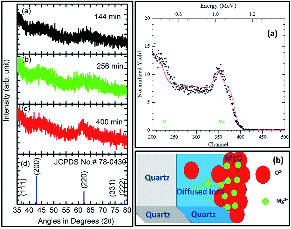 | ||
| Fig. 7 X-ray diffraction pattern of sputtered MgO for durations of: (a) 144, (b) 256, and (c) 400 min along with a reference pattern corresponding to (d) JCPDS card no 78-0430 (left panel). Right panel shows: (a) experimental (symbol) and simulated (line) Rutherford backscattering (RBS) spectra for a sputtering duration of 400 min along with (b) a schematic of the model used for simulation. | ||
At sputtering durations of 144 min and 256 min, short-range crystalline order exists as humps corresponding to (200) and (220) appear in the patterns. As MgO is deposited at sputtering times less than 256 min and is amorphous in nature; hence, XRD patterns from sputtering durations less than this were not measured. The sputtered species for a sputtering duration of 400 min exhibit long-range crystalline order in a particular direction (220); hence, the thickness at this sputtering duration was estimated. An RBS study for this sputtering duration was performed, and the results are shown in Fig. 7 (right panel). Fig. 7a (right panel) shows the simulated RBS spectrum for this sputtering duration, with the model used for the simulation shown in Fig. 7b (right panel). The model includes three layers for simulation, namely a MgO layer, MgO layer diffused to SiO2, and a SiO2 layer corresponding to an infinite thickness of substrate. The simulation parameters based on this model are collated in Table S1.† The simulation showed the formation of MgO with a thickness of ∼78 nm for a sputtering duration of 400 min.
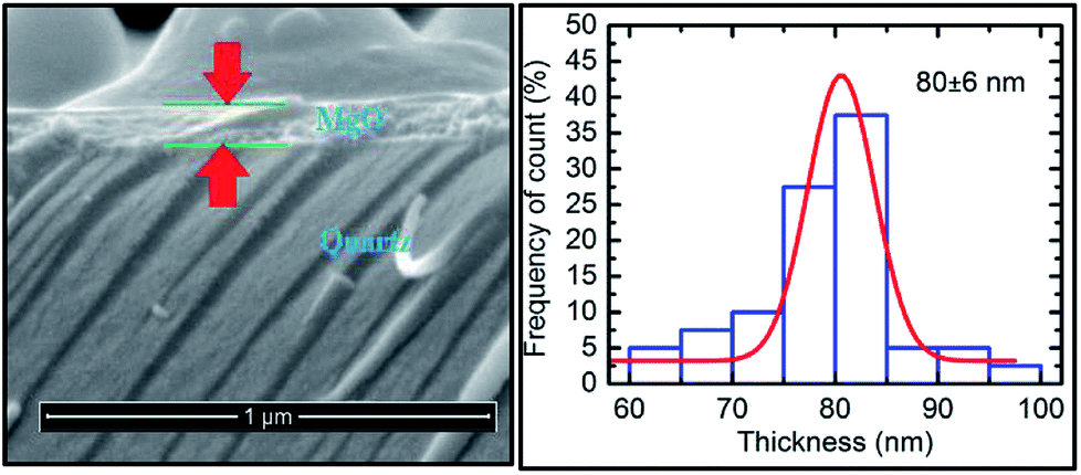
The cross-sectional SEM image for this sputtering duration showed a continuous layer on top of the substrate (Fig. 8: left panel). This measurement reveals that the thickness of the layer is 80 ± 6 nm (Fig. 8: right panel) which is close to that determined from the RBS measurements (Fig. 7: right panel).
 | ||
| Fig. 8 Cross-sectional SEM image (left panel) and thickness profile (right panel) determined for a deposition time of 400 min. | ||
Thus, the sputtered species for a duration of 400 min on fused quartz substrate reflect the characteristics of a MgO thin film with the presence of long-range crystalline order.
Annealing effect on the local electronic structure
Thus, we have successfully discussed the role of sputtering duration for the growth of MgO film when deposited using rf sputtering. We now further focus our attention on the change of the local electronic structure with annealing for the deposited film. For the discussion, we selected the film deposited at a sputtering duration of 400 min as it exhibited better crystallinity than the others. The structural behavior under annealing is shown in Fig. S6.† To determine the thickness of the annealed sputtered MgO layer, the cross-sectional SEM image is shown in Fig. 9 (left panel). The sputtered layer is more uniform compared to its not-annealed counterpart. The thickness after annealing was 71 ± 8 nm for a sputtering duration of 400 min (Fig. 9: right panel).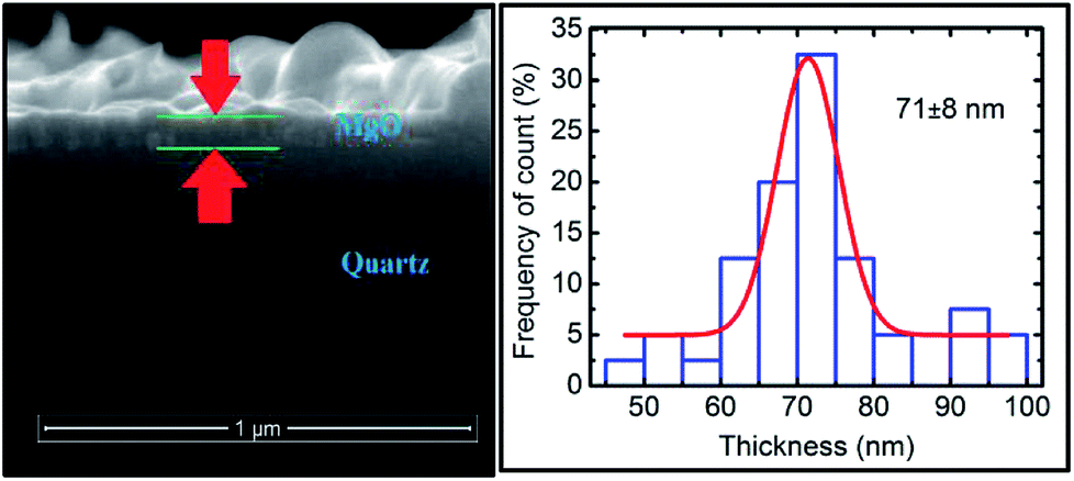 | ||
| Fig. 9 Cross-sectional SEM (left panel) and thickness profile (right panel) for annealed sputtered species with a sputtering duration of 400 min. | ||
 | ||
| Fig. 10 O K-edge spectra of: (a) as-deposited and (b) annealed film for a sputtering duration of 400 min (left panel). Spectral features are mentioned as Ao, A1, A2, A3, and A4. Pre-regions at a zoomed-in scale for: (a) as-deposited and (b) annealed films are shown in the right panels. | ||
 | ||
| Fig. 11 Mg K-edge spectra for: (a) sputtering duration of 400 min and (b) annealed counterpart in TFY mode (left panel) for different angles of measurement (15°, 25°, 45°, and 60°). Spectral features of these spectra are denoted using B1, B2, B3, B4, and B5. Differences in the spectral features for: (a) sputtering duration of 400 min and (b) annealed counterpart with the angle are shown in the right panels. | ||
The behavior of δB1B2 for the as-deposited films with the angle was a maximum for the measuring angle of 45°. This value reduces for the measuring angle of 60° (Fig. 11a: right panel). With annealing, δB1B2 increases linearly with the increase in the measuring angle for the annealed film (Fig. 11b: right panel). Thus, these results envisage a slight improvement in the crystallinity of this film as the anisotropic nature dominants in the annealed film. A similar behavior for δB1B2 was also observed for the TEY-mode measurements (Fig. 11: right panel).
Discussion
The results described in previous sections envisage the growth of MgO films with the sputtering duration. Systematic changes in the NEXAFS spectra at O K- and Mg K-edges with sputtering duration allowed us to draw a schematic of the growth process, which is shown in Fig. 12.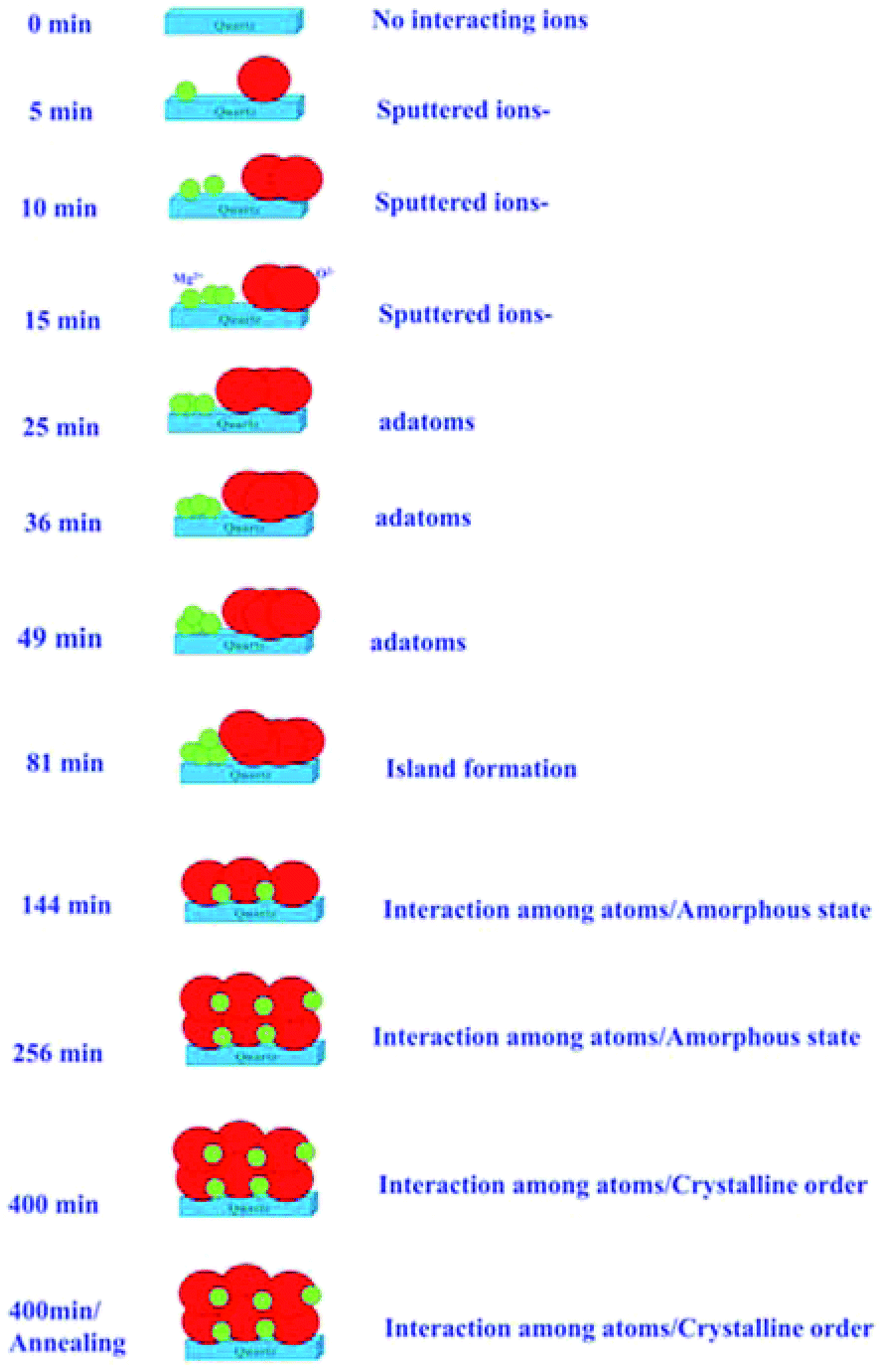 | ||
| Fig. 12 Schematic of MgO growth for various sputtering durations and for the annealed counterpart of sputtering duration of 400 min. | ||
Initially, there were no Mg2+ and O2− ions on the fused quartz substrate for a sputtering duration of 0 min. With the increase in sputtering duration, there is an increase in the population of Mg2+ and O2− ions; however, there is only a weak interaction among Mg2+ and O2− ions. With the increase in sputtering duration to 25 min, the intensity of the pre-edge peak increases. This causes an increase in the adatoms on the substrate surface; however, there is still only a weak interaction among the different ions as revealed from NEXAFS measurements. When the sputtering time is further increased to 81 min, island formation occurs. As indicated from the angle-dependent Mg K-edge and O K-edge spectra, there were no spectral features representing MgO.
As the sputtering time increases to 144 min, all the spectral features Ao, A1, A2, A3, A4 present in the O K-edge spectra. This envisages the formation of MgO unit cell; however, the XRD pattern for this sputtering duration reveals an amorphous nature. Hence, short-range ordered MgO formation is expected. The same behavior is expected for sputtering duration of 256 min. Sputtered species attain crystallization for a sputtering duration of 400 min, as can be seen from the XRD pattern at this duration. When the film with a sputtering duration of 400 min was annealed at 700 °C, the local electronic structure was improved. Thus, these measurements reveal that after a certain sputtering duration, Mg2+ ions become coordinated (Fig. 6 and 11), which is associated with the formation of a MgO unit cell.
Apart from the systematic change with the sputtering duration, NEXAFS measurements at both the O and Mg K-edges reveal strong angular dependence for sputtering durations of 5, 25, 81, 144, 256, and 400 (not-annealed and annealed counterpart) min. The existence of spectral features at different angles for these sputtering durations follow the same trend as observed in Fig. 2 and 4. Thus, these measurements further support the observations made from these figures as well as in the schematic depicted in Fig. 12; however, the spectra measured at different angles depict some specific nature in terms of the intensity. The general trend is that the spectra measured at 15° and 25° coincide, but a significant change of intensity was observed at angles of 45° and 65°. Angular dependence of the NEXAFS spectra has been extensively studied by a number of groups for wide variety of materials, including cuprates,76 vanadium oxides,77 Zn-implanted GaN,78 and ZnO.29 Further, adsorbed organic molecule on Au substrate has revealed angle dependence due to an ordered geometry on the surface.25 In the same way, adsorbed CO2 on ZnO also exhibits angular dependence due to the bond geometry, in which one O atom of CO2 is in the substrate, while second interacts with surface cation.79 Thus, the factors influencing the angular dependence of fine structures exist too with anisotropic chemical bonds, either in the structure or in the absorbed species. However, the case here is different due to the symmetric nature of the MgO crystal structure. Thus, Mg–O bond distances will be same in different directions; hence, the variation of intensity seems to be strange (Fig. 3 and 5). To corroborate this fact, we carefully went through the work reported by Luches et al.49 This study envisaged that Mg–O bond distances are different in the perpendicular and parallel directions up to a thickness of 20 monolayers (MLs). The dominant direction dependence of Mg–O bonds was observed for a film of 3 ML thickness due to intermixing with the substrate. Further, the variation of intensity of the spectral feature dominated for this thickness both in the Mg K and O K-edges. Thus, the intensity variation of spectral features is also associated with the anisotropy of chemical bonds in MgO, which is concurrent with other researchers findings working in this direction. In the case of the present work, the sputtered species on fused quartz substrate are described by three layers – (1) surface layer, (2) bulk layer, (3) MgO intermixed with SiO2.80 Thus, the factors that influence the bond distance are unsaturated bonds at surface and bonds formed in the intermixed layers. Moreover, the formation of an island-like region cannot be ignored as it will increase sufficiently the number of unsaturated bonds. Hence, the angular dependence is associated with the presence of Mg–O bonds with different bond distances in different directions. The enhanced intensity of the spectrum for higher angles, like 45° and 65°, is due to passing through the sputtered species rather than deep in these species, which thus leads to detecting a greater number of scatters. This effect is also evident from the dominancy of this behavior for lower sputtering durations.
Conclusions
The present work reveals the formation of MgO on an amorphous fused quartz substrate, which was investigated using near-edge X-ray absorption fine structure measurements. These measurements were systematically carried out for various sputtering durations ranging from 5 min to 400 min. We have shown that these measurements are able to provide a complete account for the growth mechanism. One can clearly observe the change of Mg2+ ion coordination as well as molecular oxygen with the changing sputtering duration. These measurements clearly reflect the situation where interactions among the ions of MgO really take place.Conflicts of interest
Authors declare no conflicts of interests.Acknowledgements
This work was supported by Korea Institute of Science and Technology, Seoul, Korea (KIST Project No. 2V06030).Notes and references
- J. L. Robins, Appl. Surf. Sci., 1998, 33–34, 379–394 Search PubMed.
- J. A. Venables, G. D. T. Spiller and M. Hanbucken, Rep. Prog. Phys, 1988, 47, 399–459 CrossRef.
- K. Reichelt, Vacuum, 1988, 38, 1083–1099 CrossRef.
- F. L. Forgerini and R. Marchiori, Biomatter., 2014, 4, e28871 CrossRef PubMed.
- I. Petrov, P. B. Barna, L. Hultman and J. E. Greene, J. Vac. Sci. Technol., A, 2003, 21, S117–S127 CrossRef.
- von Keudell, Plasma Sources Sci. Technol., 2000, 9, 455–467 CrossRef.
- B. B. Sahu, J. G. Han and H. Kersten, Phys. Chem. Chem. Phys., 2017, 19, 5591–5610 RSC.
- H. Haberland, Z. Insepov and M. Moseler, Phys. Rev. B: Condens. Matter Mater. Phys., 1995, 51, 11061–11067 CrossRef.
- J. R. Levine, J. B. Cohen, Y. W. Chung and P. Georgopoulos, J. Appl. Crystallogr., 1989, 22, 528–532 CrossRef.
- P. Kratzer, E. Penev and M. Scheffler, Appl. Surf. Sci., 2003, 216, 436–446 CrossRef.
- T. S. Rahman, C. Ghosh, O. Trushin, A. Kara and A. Karim, Proc. SPIE Annual Meeting 2004, vol. 1, p. 5509 Search PubMed.
- V. M. Jiménez, J. P. Espinós and A. R. González-Elipe, Appl. Surf. Sci., 1999, 141, 186–192 CrossRef.
- F.-J. Meyer zu Heringdorf, M. C. Reuter and R. M. Tromp, Nature, 2001, 412, 517–520 CrossRef PubMed.
- J. Yang, S. Yim and T. S. Jones, Sci. Rep., 2015, 5, 9441 CrossRef PubMed.
- P. Sunderberg and M. Karppinen, Beilstein J. Nanotechnol., 2014, 5, 1104–1136 CrossRef PubMed.
- Y. Wu, H. Chou, H. Ji, Q. Wu, S. Chen, W. Jiang, Y. Hao, J. Kang, Y. Ren, R. D. Piner and R. S. Ruoff, ACS Nano, 2012, 6, 7731–7738 CrossRef PubMed.
- C. Chen, Z. Feng, Y. Feng, Y. Yue, C. Qin, D. Zhang and W. Feng, ACS Appl. Mater. Interfaces, 2016, 8, 19004–19011 CrossRef PubMed.
- E. I. Rogacheva, S. N. Grigorov, O. N. Nashchekina, T. V. Tavrina, S. G. Lyubchenko, A. Yu. Sipatov, V. V. Volobuev, A. G. Fedorov and M. S. Dresselhaus, Thin Solid Films, 2005, 493, 41–48 CrossRef.
- J. P. Singh, B. Kaur, S. Gautam, W. C. Lim, K. Asokan and K. H. Chae, Superlattices Microstruct., 2016, 100, 560–586 CrossRef.
- W. X. Wang, Y. Yang, H. Naganuma, Y. Ando, R. C. Yu and X. F. Han, Appl. Phys. Lett., 2011, 99, 012502 CrossRef.
- C. S. Schnohr and M. C. Ridgway, Introduction to X-Ray Absorption Spectroscopy, in X-Ray Absorption Spectroscopy of Semiconductors, ed. C. S. Schnohr and M. C. Ridgway, Springer Series in Optical Sciences, 2015, vol. 190, DOI:10.1007/978-3-662-44362-0_1.
- F. de Groot, G. Vankó and P. Glatzel, J. Phys.: Condens. Matter, 2009, 21, 104207 CrossRef PubMed.
- C. X. Kronawitter, J. R. Bakke, D. A. Wheeler, W. C. Wang, C. Chang, B. R. Antoun, J. Z. Zhang, J. Guo, S. F. Bent, S. S. Mao and L. Vayssieres, Nano Lett., 2011, 11, 3855–3861 CrossRef PubMed.
- A. D. Dwivedi, N. D Sanandiya, J. P. Singh, S. M. Husnain, K. H. Chae, D. S. Hwang and Y. S. Chang, ACS Sustainable Chem. Eng., 2017, 5, 518–528 CrossRef.
- L. Cao, W. H. Zhang, Y. Y. Han, T. X. Chen, Z. Y. Zheng, L. Wan, F. Q. Xu, K. Ibrahim, H. J. Qian and J. O. Wang, Chin. Sci. Bull., 2011, 56, 3575–3577 CrossRef.
- J. H. Guo, L. Vayssieres, C. Persson, R. Ahuja, B. Johansson and J. Nordgren, J. Phys.: Condens. Matter, 2002, 14, 6969 CrossRef.
- B. Zhang, J. Chen, P. Yang, X. Chi, W. Lin, T. Venkatesan, C. J. Sun, S. M. Heald and G. M. Chow, Sci. Rep., 2016, 6, 19886 CrossRef PubMed.
- Y. Ufuktepe, G. Akgul, F. Aksoy and D. Nordlund, X-Ray Spectrom., 2011, 40, 427–431 CrossRef.
- J. W. Chiou, J. C. Jan, H. M. Tsai, C. W. Bao, W. F. Pong, M. H. Tsai, I. H. Hong, R. Klauser, J. F. Lee, J. J. Wu and S. C. Liu, Appl. Phys. Lett., 2004, 84, 3462–3464 CrossRef.
- R. P. Gandhiraman, D. Nordlund, C. Javier, J. E. Koehne, B. Chen and M. Meyyappan, J. Phys. Chem. C, Nanomater. Interfaces, 2014, 118, 18706–18712 CrossRef PubMed.
- J. P. Singh and K. H. Chae, Condens. Matter, 2017, 2, 36 CrossRef.
- N. Pathak, S. K. Gupta, C. L. Prajapat, S. K. Sharma, P. S. Ghosh, B. Kanrar, P. Kumar Pujari and R. M. Kadam, Phys. Chem. Chem. Phys., 2017, 19, 11975–11989 RSC.
- J. Li, Y. Jiang, Y. Li, D. Yang and M. Yan, Appl. Phys. Lett., 2013, 102, 072406 CrossRef.
- F. Gao, J. Hu, C. Yang, H. Qin, L. Sun, X. Kong and M. Jiang, Solid State Commun., 2009, 149, 855–856 CrossRef.
- N. Pathak, P. S. Ghosh, S. K. Gupta, R. M. Kadam and A. Arya, RSC Adv., 2016, 6, 96398–96415 RSC.
- J. P. Singh, S. O. Won, W. C. Lim, C. H. Chim and K. H. Chae, Mater. Lett., 2017, 198, 34–37 CrossRef.
- J. P. Singh, S. H. Kim, H. K. Kang, S. O. Won, I. J. Lee and K. H. Chae, Mater. Chem. Front., 2018, 2, 1707–1715 RSC.
- Y. Z. Wu, A. K. Schmid and Z. Q. Qiu, Phys. Rev. Lett., 2006, 97, 217205 CrossRef PubMed.
- C. Dias, L. M. Guerra, B. D. Bordalo, H. Lv, A. M. Ferraria, A. M. Botelho do Rego, S. Cardoso, P. P. Freitas and J. Ventura, Phys. Chem. Chem. Phys., 2017, 19, 10898–10904 RSC.
- T. Uchino and D. Okutsu, Phys. Rev. Lett., 2008, 101, 117401 CrossRef PubMed.
- M. Franke, D. Wechsler, Q. Tariq, M. Röckert, L. Zhang, P. K. Thakur, N. Tsud, S. Bercha, K. C. Prince, T.-L. Lee, H.-P. Steinrck and O. Lytken, Phys. Chem. Chem. Phys., 2017, 19, 11549–11553 RSC.
- X.-H. Shi, J.-J. Ban, L. Zhang, Z.-P. Sun, D.-Z. Jia and G.-C. Xu, RSC Adv., 2017, 7, 16189–16195 RSC.
- S.-I. Jo, Y.-I. An, K.-Y. Kim, S.-Y. Choi, J.-S. Kwak, K.-R. Oh and Y.-U. Kwon, Phys. Chem. Chem. Phys., 2017, 19, 6224–6232 RSC.
- I. V. Mishakov, A. Bedilo, R. M. Richards, V. V. Chesnokov, A. M. Volodin, V. I. Zaikovskii, R. A. Buyanov and K. J. Klabunde, J. Catal., 2002, 206, 40–48 CrossRef.
- J. P. Singh, M. Jung Ji, M. Kumar, I.-J. Lee and K. Hwa Chae, J. Alloys Compd., 2018, 748, 355–362 CrossRef.
- J. P. Singh, W. C. Lim, S. O. Won, I. J. Lee and K. Hwa Chae, Manipulating surface local electronic structure of MgO, Proc. of Korean Vacuum Society Conference, 2017, vol. 2, pp. 143–144 Search PubMed.
- S. Ogawa, S. Murakami, K. Shirai, K. Nakanishi, T. Ohta and S. Yagi, J. Phys.: Conf. Ser., 2013, 417, 012065 CrossRef.
- S. Ogawa, H. Niwa, K. Nakanishi, T. Ohta and S. Yagi, J. Surf. Anal., 2011, 17, 319–323 CrossRef.
- P. Luches, S. D'Addato, S. Valeri, E. Groppo, C. Prestipino, C. Lamberti and F. Boscherini, Phys. Rev. B: Condens. Matter Mater. Phys., 2004, 69, 045412 CrossRef.
- J. A. Rodriguez, T. Jirsak, A. Freitag and J. Z. Larese, J. Phys. Chem. B, 2000, 104, 7439–7448 CrossRef.
- X. L. Tong, D. S. Jiang, W. B. Hu, Z. M. Liu and M. Z. Luo, Appl. Phys. A: Mater. Sci. Process., 2006, 84, 143–148 CrossRef.
- K. Matsuzak, H. Hosono and T. Susak, Phys. Rev. B: Condens. Matter Mater. Phys., 2010, 82, 033408 CrossRef.
- F. Niu, B. H. Hoerman and B. W. Wessels, J. Vac. Sci. Technol., B: Microelectron. Nanometer Struct.--Process., Meas., Phenom., 2000, 18, 2146–2152 CrossRef.
- M. Putkonen, T. Sajavaarab and L. NiinistoÈ, J. Mater. Chem., 2000, 10, 1857–1861 RSC.
- E. Buer, A. K. Green and K. M. Kunz, Appl. Phys. Lett., 1966, 8, 248–249 CrossRef.
- Y. Kaneko, N. Mikoshiba and T. Yamashita, Jpn. J. Appl. Phys., 1991, 30, 1091 CrossRef.
- M. Terauchi, J. Hashimoto, H. Nishitani, Y. Fukui, M. Okafuji, H. Yamashita, H. Hayata, T. Okuma, H. Yamanishi, M. Nishitani and M. Kitagawa, J. Soc. Inf. Disp., 2008, 16, 1195–1200 CrossRef.
- J. P. Singh, M. Kumar, I. J. Lee and K. H. Chae, Appl. Sci. Lett., 2017, 3, 47–52 Search PubMed.
- H. N. Hwang, H. S. Kim, B. Kim, C. C. Hwang, S. W. Moon, S. M. Chung, C. Jeon, C. Y. Park, K. H. Chae and W. K. Choi, Nucl. Instrum. Methods Phys. Res., Sect. A, 2007, 581, 850–855 CrossRef.
- J. P. Singh, S. Gautam, W. C. Lim, K. Asokan, B. Bhusan Singh, M. Raju, S. Chaudhary, D. Kabiraj, D. Kanjilal, J.-M. Lee, J.-M. Chen and K. Hwa Chae, Vacuum, 2017, 138, 48–54 CrossRef.
- M. Abbate, J. B. Goedkoop, F. M. F. de Groot, M. Grioni, J. C. Fuggle, S. Hofmann and H. P. M. Sacchi, Surf. Interface Anal., 1992, 18, 65–69 CrossRef.
- A. J. Achkar, T. Z. Regier, H. Wadati, Y.-J. Kim, H. Zhang and D. G. Hawthorn, Phys. Rev. B: Condens. Matter Mater. Phys., 2011, 83, 129901 CrossRef.
- D. Asakura, E. Hosono, Y. Nanba, H. Zhou, J. Okabayashi, C. Ban, P.-A. Glans, J. Guo, T. Mizokawa, G. Chen, A. J. Achkar, D. G. Hawthron, T. Z. Regier and H. Wadati, AIP Adv., 2016, 6, 035105 CrossRef.
- Q. Yang, Nucl. Instrum. Methods Phys. Res., Sect. B, 1994, 90, 602–605 CrossRef.
- J. P. Singh, W. C. Lim, S. Gautam, K. Asokan and K. H. Chae, Mater. Des., 2016, 101, 72–79 CrossRef.
- J. P. Singh, W. C. Lim, I. J. Lee, S. O. Won and K. H. Chae, Sci. Adv. Mater., 2018, 10, 1372–1376 Search PubMed.
- J. G. Chen, Surf. Sci. Rep., 1997, 30, 1–152 CrossRef.
- A. Nilsson, D. Nordlund, I. Waluyo, N. Huang, H. Ogasawara, S. Kaya, U. Bergmann, L.-Å. Näslund, H. Öström, Ph. Wernet, K. J. Andersson, T. Schiros and L. G. M. Pettersson, J. Electron Spectrosc. Relat. Phenom., 2010, 177, 99–129 CrossRef.
- H. Werner, Th. Schedel-Niedrlg, M. Wohlers, D. Herein, B. Herzog, R. Schlogl, M. Keil, A. M. Bradshaw and J. Kirschner, J. Chem. Soc., Faraday Trans., 1994, 90, 403–409 RSC.
- J. Hrbek, T. K. Sham, M. L. Shek and G. Q. Xu, Langmuir, 1992, 8, 2461–2472 CrossRef.
- O. Baseggio, M. Romeo, G. Fronzoni and M. Stener, Surf. Sci., 2013, 616, 178–185 CrossRef.
- O. Y. Khyzhun, T. Strunskus, Ch. Wöll, H. Gies and V. Staemmler, J. Chem. Phys., 2008, 129, 084711–084719 CrossRef PubMed.
- T. Lindner, H. Sauer, W. Engel and K. K. Kambe, Phys. Rev. B: Condens. Matter Mater. Phys., 1986, 33, 22–24 CrossRef.
- T. Mizoguchi, I. Tanaka, M. Yoshiya, F. Oba, K. Ogasawara and H. Adachi, Phys. Rev. B, 2000, 61, 2180–2187 CrossRef.
- J. P. Singh, W. C. Lim, J. Lee, J. Song and K. H. Chae, Appl. Surf. Sci., 2018, 432, 131–139 CrossRef.
- A. Balzarotti, F. Arciprete, S. Colonna, M. Diociaiuti, F. Patella and M. De Crescenzi, Phys. C, 1993, 218, 301–308 CrossRef.
- E. Goering, O. Milller, M. L. denBoer and S. Horn, Phys. B, 1994, 194–196, 1217–1218 CrossRef.
- J. W. Chiou, S. Mookerjee, K. V. R. Rao, J. C. Jan, H. M. Tsai, K. Asokan, W. F. Pong, F. Z. Chien, M.-H. Tsai, Y. K. Chang, Y. Y. Chen, J. F. Lee, C. C. Lee and G. C. Chi, Appl. Phys. Lett., 2002, 81, 3389–3391 CrossRef.
- R. Davis, J. F. Walsh, C. A. Muryn, G. Thornton, V. R. Dhanak and K. C. Prince, Surf. Sci. Lett., 1993, 298, L196–L202 CrossRef.
- A. Sarkar, T. Ashraf, W. Grafeneder and R. Koch, J. Phys.: Condens. Matter, 2018, 30, 155001 CrossRef PubMed.
Footnote |
| † Electronic supplementary information (ESI) available. See DOI: 10.1039/c8ra02873g |
| This journal is © The Royal Society of Chemistry 2018 |