 Open Access Article
In situ tuning of crystallization pathways by electron beam irradiation and heating in amorphous bismuth ferrite films†
Zhipeng Lia,
Zhong Lin Wang *abc and
Zhiwei Wang
 *ab
*ab
aBeijing Institute of Nanoenergy and Nanosystems, Chinese Academy of Sciences, Beijing 100083, P. R. China. E-mail: wangzhiwei@binn.cas.cn
bSchool of Nanoscience and Technology, University of Chinese Academy of Sciences, Beijing 100049, P. R. China
cSchool of Materials Science and Engineering, Georgia Institute of Technology, Atlanta, Georgia 30332-0245, USA. E-mail: zlwang@gatech.edu
First published on 28th June 2018
Abstract
The sculpting of crystalline materials from amorphous films by electron beam irradiation in transmission electron microscopy (TEM) offers an effective way for fabrication of nanostructure and devices. However, the synthesis of multifunctional complex oxide and related composites for possible device application is difficult to achieve. Here, we show that the crystallization pathways of amorphous bismuth ferrite films could be tuned by controlled electron beam irradiation and in situ heating in TEM. The results show that Bi segregates from amorphous films and then aggregates into crystalline nanoparticles (the particle size can be tuned by electron dose rates) under electron beam irradiation below 100 °C, while Bi2Fe4O9 nanocrystals are observed at boundary areas between quasi-liquid Bi nanoparticles at 300 °C due to the cooperative effect of electron beam irradiation and thermal heating. Moreover, the Bi/Bi2Fe4O9 metal/semiconductor solid state heterostructure with nearly atomically sharp interfaces emerges when cooling down to room temperature. This finding expands the variety of nanostructures synthesized by electron bombardment and offers a new way to fabricate complex architectures and possible functional devices at the nanometer scale with direct in situ TEM observation and monitoring.
1 Introduction
An accurate synthesis and manipulation of materials is essential for the building up of device structure at the nanoscale with advanced functionalities. Besides atomic manipulation by scanning tunneling microscopy (STM) and electron beam lithography in scanning electron microscopy (SEM), it has been shown that the localized amorphous to crystalline transition induced by controlled energetic beams offers new opportunities for nanostructure synthesis and nanofabrication.1–6 The electron beam inside a transmission electron microscope (TEM) can be focused as small as a single atomic column, providing a platform for atomic resolution imaging, diffraction and chemical analysis with the advantage of an atomically confined electron beam–material interaction volume. Recently, atomic-level sculpting of a 3D crystalline complex oxide (SrTiO3) nanostructure from amorphous films in a scanning TEM was demonstrated.7With the wealth of electron–matter interaction mechanisms, such as knock-on displacement and oxide reduction, a variety of nanostructures including nanoparticles, nanowires and two-dimensional materials can be fabricated under controlled conditions in TEM.8 One example is the formation of metallic nanoparticles (Bi, Ag, Mn etc.) by irradiation of a condensed electron beam.9–12 However, the in situ synthesis of complex oxides and oxide/metal composite nanostructures with rich functionalities is rarely reported, which may require well controlled irradiation and additional stimulus, such as environment atmosphere control or thermal heating.13,14
In our in situ investigation, a high resolution TEM (HRTEM) is used to track the crystallization dynamics and crystalline fluctuations. We demonstrate that the crystallization pathways can be tuned from amorphous bismuth ferrite films by electron beam irradiation and in situ heating in TEM. The results reveal that Bi nanocrystals form by electron beam irradiation below 100 °C, while crystalline Bi2Fe4O9 is observed at the boundaries of liquid-state Bi nanoparticles at 300 °C. The heterostructure with highly crystalline Bi nanoparticles/Bi2Fe4O9 can be synthesized when cooling down to room temperature. This finding indicates that the variety of in situ synthesized nanostructures can be further expanded by electron irradiation and in situ techniques, especially thermal heating in TEM, paving a new way for the accurate fabrication of complex architectures at the nanoscale for functional applications such as high efficient photocatalysis and photoelectric devices.
2 Experimental
The amorphous bismuth ferrite thin films were prepared by pulsed laser deposition method with excimer laser (with wavelength of 248 nm) at room temperature. The polycrystalline ceramic with composition of Bi1.1FeO3 (from Kurt Lesker company) was used as target. The laser energy density on the target was ∼1 J cm−2, the repetition rate was 4 Hz and the deposition time was 10 minutes. The samples were directly deposited onto silicon nitride membranes in DENSsolutions heating chips (see ESI Fig. S1†) at room temperature with oxygen pressure of 100 mtorr. High resolution transmission electron microscopy (HRTEM), high angle annular dark field scanning TEM (HAADF-STEM) and energy dispersive X-ray spectroscopy (EDS) were performed on a FEI Tecnai F20 with a field emission gun at acceleration voltage of 200 kV.3 Results and discussion
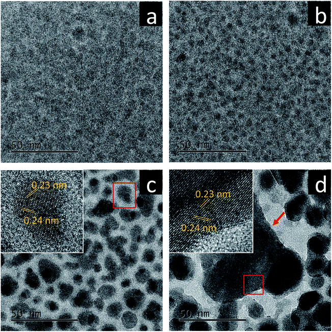
As electron dose rates, not total electron doses, usually play deterministic roles in promoting crystallization processes including both nucleation and growth of nanocrystals,15–17 we systematically studied the effect of electron dose rates on the crystallization of amorphous bismuth ferrites prepared using a pulsed laser deposition technique. Fig. 1 shows TEM images of the amorphous films (whose chemical formula is Bi3.8FeOx according to EDS characterization in Fig. S1†) acquired after electron beam irradiation of 15 min with various electron dose rates at room temperature (RT). When a very low dose rate (12 e (Å2 s)−1) is used, no obvious morphological/structural variation is present in the amorphous films after the irradiation (Fig. 1a). In contrast, closely-packed nanoparticles form when the dose rates reach to 1.2 × 10³ e (Å2 s)−1 and above (Fig. 1b–d). Also, the nanoparticle sizes monotonically increase with electron dose rates, suggesting higher driving forces produced by stronger electron beams for promoting the growth of nanoparticles. A further investigation reveals different crystallographic characteristics of the nanoparticles in between Fig. 1b and Fig. 1c and d. The former has an average diameter less than 4.4 nm and features still amorphous configurations, while the latter displays rather clearly crystalline structures. HRTEM imaging (Fig. 1c and d, insets) shows the interplanar spacings of 0.23 nm and 0.24 nm, which could be assigned to (110) and (104) planes of rhombohedral Bi metal (space group: R![[3 with combining macron]](https://www.rsc.org/images/entities/char_0033_0304.gif) m), respectively. EDS analysis was also performed to investigate further the new nanostructures formed after the electron bombardments (see ESI Fig. S2†), which illustrates that the nanoparticles are Bi-enriched while Fe and O are driven to the boundaries between nanoparticles. Fig. 1d also indicates that very violent electron bombardment (1.2 × 10⁵ e (Å2 s)−1) could lead to the occurrence of explosive crystallization,18,19 in which a very large, triangular-like nanoparticle is formed with ∼60 nm sides.
m), respectively. EDS analysis was also performed to investigate further the new nanostructures formed after the electron bombardments (see ESI Fig. S2†), which illustrates that the nanoparticles are Bi-enriched while Fe and O are driven to the boundaries between nanoparticles. Fig. 1d also indicates that very violent electron bombardment (1.2 × 10⁵ e (Å2 s)−1) could lead to the occurrence of explosive crystallization,18,19 in which a very large, triangular-like nanoparticle is formed with ∼60 nm sides.
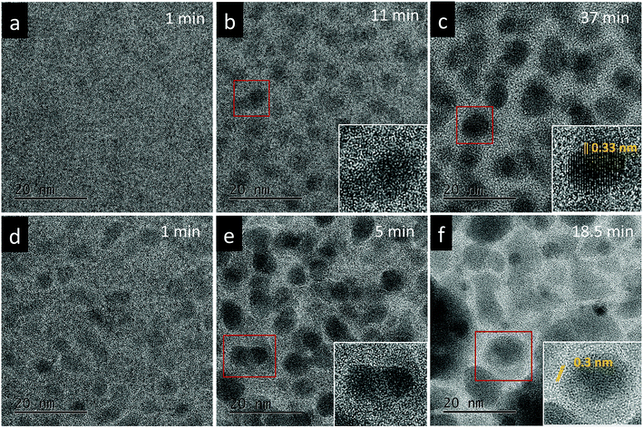
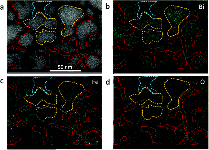
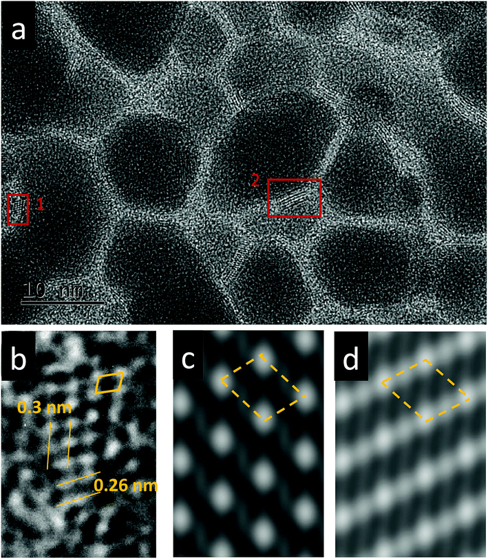
The effect of thermal heating on the crystallization of the amorphous films was subsequently investigated in combination with gentle electron irradiations. The moderate electron dose rates (close to the value used in Fig. 1b) have been employed for the heating observations because, with such level of dose rates, the films can go through a certain degree of morphological variation at room temperature, but no significant and fast crystallizations occur. This facilitates a direct comparison and analysis of the influences of various annealing temperatures (up to 300 °C). Fig. 2a–c displays several time-sequential TEM images recorded after the film has been heated to 100 °C, which shows that Bi-enriched particles nucleate, grow and coalesce with neighbor ones, and gradually form crystalline structures (the interplanar spacing of 0.33 nm in Fig. 2c inset is consistent with the (012) plane of Bi metal). The phenomenon resembles what has been observed on the sample at room temperature and with high electron dose rates (Fig. 1c). When temperature was elevated to 300 °C (Fig. 2d–f), we see the rapid emergence of high-density nanoparticles, followed by the steady growth and coalescence. However, the nanoparticles now feature amorphous-like structure, while the boundaries transform from amorphous to crystalline state (with lattice spacing of 0.3 nm) as the particles sizes increase and the boundaries become narrower. Fig. 3 shows EDS mapping of the new nanostructures formed at the 300 °C heating. It can be seen that the narrow boundaries between nanoparticles feature Fe enriched. HRTEM imaging and simulations are also performed to identify atomic structures and phases of the nanocrystals at boundaries, as shown in Fig. 4. Fig. 4b shows an enlarged view of the nanocrystal 1 in Fig. 4a, in which the lattice fringes with planar distances of 0.3 nm and 0.26 nm are consistent with the (1![[2 with combining macron]](https://www.rsc.org/images/entities/char_0032_0304.gif) 1) and (112) planes in orthorhombic mullite-type Bi2Fe4O9 (space group: Pbam). Further multislice HRTEM simulation (Fig. 4c) using the structural model of Bi2Fe4O9 (with zone axis of [5 1
1) and (112) planes in orthorhombic mullite-type Bi2Fe4O9 (space group: Pbam). Further multislice HRTEM simulation (Fig. 4c) using the structural model of Bi2Fe4O9 (with zone axis of [5 1 ![[3 with combining macron]](https://www.rsc.org/images/entities/char_0033_0304.gif) ], defocus of −90 nm and sample thickness of 17.7 nm) matches well the experimental result (Fig. 4b). The HRTEM lattice fringes at region 2 in Fig. 4a could be assigned to (1
], defocus of −90 nm and sample thickness of 17.7 nm) matches well the experimental result (Fig. 4b). The HRTEM lattice fringes at region 2 in Fig. 4a could be assigned to (1![[2 with combining macron]](https://www.rsc.org/images/entities/char_0032_0304.gif) 1) plane of Bi2Fe4O9 structure, which agrees well with the HRTEM simulation shown in Fig. 4d.
1) plane of Bi2Fe4O9 structure, which agrees well with the HRTEM simulation shown in Fig. 4d.
The study illustrates clearly that phase segregation is commonly present in the new nanoscale objects formed either through high-dose-rate electron irradiations (at room temperature) or high-temperature heating with moderate electron beams. Specifically, driven by electron irradiation and/or thermal heating, the originally uniform amorphous bismuth ferrite films finally turn into high-density Bi-enriched nanoparticles interconnected by Fe + O enriched nanostructures (see the EDS maps in Fig. 3 and ESI Fig. S2†). We suggest that the occurrence of phase segregations relate to the following two factors. First, the rather low-content Fe in the amorphous films (Bi![[thin space (1/6-em)]](https://www.rsc.org/images/entities/char_2009.gif) :
:![[thin space (1/6-em)]](https://www.rsc.org/images/entities/char_2009.gif) Fe is ∼3.8
Fe is ∼3.8![[thin space (1/6-em)]](https://www.rsc.org/images/entities/char_2009.gif) :
:![[thin space (1/6-em)]](https://www.rsc.org/images/entities/char_2009.gif) 1) may facilitate Bi aggregation. This can be identified further by preparing stoichiometric or Fe-enriched bismuth ferrite films in the future. Second, electron beam irradiation could lead to film decomposition by way of the Knotek–Feibelman (K–F) mechanism. According to the mechanism, highly energetic electron beams can ionize the cations and create vacant electronic states which can be filled by the electrons from valence band of O anions by way of (interatomic) Auger decay, leading to the formation of O+ or neutral O. The Madelung potential by surrounding cations turns repulsive to the positive charged anions, and as a consequence, the oxygen atoms get desorbed from the specimen. Gradually, Bi–O bonds are replaced by Bi–Bi bonds in an amorphous configuration.20 The energy transfer to sample from the continuous electron beam irradiation and/or thermal heating can increase the atomic mobility and sample temperature which could serve as the driving force for the crystallization of Bi nanoparticles, as shown in Fig. 1c and d and 2c.21 We measured/compared the atomic ratios of O to Bi + Fe (cations) between initial amorphous film (O/cations)initial and post-irradiation region (O/cations)post based on the data shown in ESI Fig. S1d and S2e,† which results in a ratio value of 0.9 using the simple formula (O/cations)post/(O/cations)initial. This indicates that relatively 10% of oxygen is lost after electron beam irradiation. Thus, the EDS analysis provides a good support for the K–F mechanism. In addition to the K–F mechanism, there may be other influence factors which could also contribute to the specimen damage more or less, such as electron beam induced heating and sputtering.22
1) may facilitate Bi aggregation. This can be identified further by preparing stoichiometric or Fe-enriched bismuth ferrite films in the future. Second, electron beam irradiation could lead to film decomposition by way of the Knotek–Feibelman (K–F) mechanism. According to the mechanism, highly energetic electron beams can ionize the cations and create vacant electronic states which can be filled by the electrons from valence band of O anions by way of (interatomic) Auger decay, leading to the formation of O+ or neutral O. The Madelung potential by surrounding cations turns repulsive to the positive charged anions, and as a consequence, the oxygen atoms get desorbed from the specimen. Gradually, Bi–O bonds are replaced by Bi–Bi bonds in an amorphous configuration.20 The energy transfer to sample from the continuous electron beam irradiation and/or thermal heating can increase the atomic mobility and sample temperature which could serve as the driving force for the crystallization of Bi nanoparticles, as shown in Fig. 1c and d and 2c.21 We measured/compared the atomic ratios of O to Bi + Fe (cations) between initial amorphous film (O/cations)initial and post-irradiation region (O/cations)post based on the data shown in ESI Fig. S1d and S2e,† which results in a ratio value of 0.9 using the simple formula (O/cations)post/(O/cations)initial. This indicates that relatively 10% of oxygen is lost after electron beam irradiation. Thus, the EDS analysis provides a good support for the K–F mechanism. In addition to the K–F mechanism, there may be other influence factors which could also contribute to the specimen damage more or less, such as electron beam induced heating and sputtering.22
The amorphous-like structural configurations of Bi nanoparticles formed during high-temperature heating (Fig. 4) can be easily understood by considering the rather low melting point of Bi (271.3 °C). It is highly likely that the film heated to 300 °C led to the transformation of Bi nanoparticles from solid state to quasi-liquid state. During the growth of liquid-like Bi nanoparticles, Fe and O atoms gradually segregate to the boundary areas, where amorphous Bi2Fe4O9 nanostructures may be formed initially, and then followed by the crystallizations. The electron beam induced charging effect might play a role in forming the final structural configurations. The bismuth nanoparticles featuring high electrical resistance may be susceptible to charge accumulation, resulting in repulsive forces between nanoparticles which could help keep their monodispersity instead of coalescing. Given that no Bi2Fe4O9 nanocrystals have been observed at boundaries when the film was excited by pure electron irradiations without heating (see Fig. 1), the reasonable conclusion can thus be drawn that the crystallization should be mediated by the formation of liquid-state Bi nanoparticles. This highlights the coordinative effect of electron beam and thermal heating on the generation of complex nanostructures.
It is worth mentioning that the dynamical fluctuations of Bi2Fe4O9 nanostructures are sometimes observed during the thermal heating at 300 °C, including the transformations from crystalline to amorphous states of the nanocrystals (see ESI Fig. S3†). The top limit of the potential barrier for amorphous to crystalline transition (referred to as Ep) by electron beam irradiation may be expressed as:
| Ep = Ec − Es + Ead |
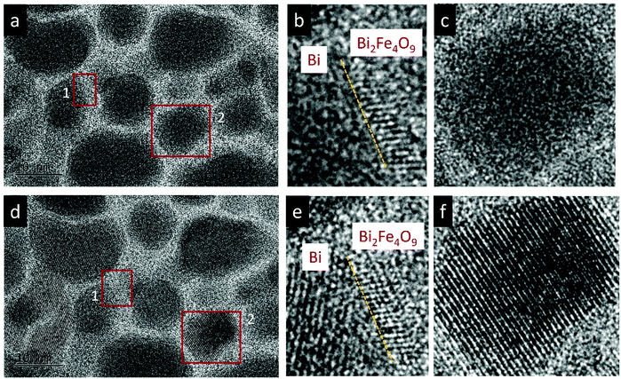
When the sample annealed at 300 °C is cooled down to room temperature, as shown in Fig. 5, the quasi-liquid Bi particles transform back to crystalline state while the Bi2Fe4O9 nanocrystals stay stable, resulting in Bi/Bi2Fe4O9 heterostructures in solid state. The nearly atomically sharp interface present in HRTEM imaging (Fig. 5e) may indicate the coherent contact between these two materials during the condensation/crystallization of Bi-enriched nanoparticles from quasi-liquid state driven by the degree of undercooling. As known, Bi2Fe4O9 is a semiconductor, and the metal Bi exhibits unique transport properties including long carrier mean free path and small carrier effective mass. Thus, the metal/semiconductor junctions (Bi/Bi2Fe4O9) featuring sharp interfaces created by the combined electron beam irradiation and thermal heating approach may find valuable applications in the photocatalysis and optoelectronics, etc.24–26
4 Conclusions
We demonstrate that the crystallization pathways can be in situ tuned by electron beam irradiation and thermal heating using amorphous bismuth ferrite films as an example. Direct electron beam irradiation can result in the formation of Bi-enriched nanocrystals with particle size controlled by electron doses. When combining with film annealing at 300 °C, we observed the formation of crystalline Bi2Fe4O9 nanostructures at the boundaries between quasi-liquid Bi nanoparticles. Both stable states and structural fluctuations of Bi2Fe4O9 nanocrystals are observed under electron beam irradiation and heating. Furthermore, the subsequent temperature decrease leads to the formation of Bi/Bi2Fe4O9 heterostructures with approximately atomically sharp interfaces at room temperature. This finding provides an insight to in situ synthesis with direct observation and monitoring of metal/semiconductor nanoarchitecture by electron beam irradiation and thermal heating at nanometer scale.Conflicts of interest
There are no conflicts of interest to declare.Acknowledgements
This research was supported by National Key R & D Program of China (2016YFA0202701), “Thousands Talents” Program for pioneer researcher and his innovation team, National Natural Science Foundation of China (Grant No. 51602025), and the Fundamental Research Funds for the Central Universities (Grant No. FRF-TP-17-043A1). We thank Prof. Jing Zhu for valuable discussions and the National Electron Microscopy Centre (Beijing) in Tsinghua University for growth of thin film samples.References
- D. K. Schweizer and E. K. Eigler, Nature, 1990, 344, 524 CrossRef.
- A. N. Broers, A. C. F. Hoole and J. M. Ryan, Microelectron. Eng., 1996, 32, 131 CrossRef.
- S. J. Pennycook P. D. Nellist, Scanning Transmission Electron Microscopy: Imaging and Analysis, Springer 2011, 762 Search PubMed.
- J. H. Lin, O. Cretu, W. Zhou, K. Suenaga, D. Prasai, K. I. Bolotin, N. T. Cuong, M. Otani, S. Okada, A. R. Lupini, J.-C. Idrobo, D. Caudel, A. Burger, N. J. Ghimire, J. Yan, D. G. Mandrus, S. J. Pennycook and S. T. Pantelides, Nat. Nanotechnol., 2014, 9, 436 CrossRef PubMed.
- P. Y. Huang, S. Kurasch, J. S. Alden, A. Shekhawat, A. A. Alemi, P. L. McEuen, J. P. Sethna, U. Kaiser and D. A. Muller, Science, 2013, 342, 224 CrossRef PubMed.
- S. V. Kalinin, A. Borisevich and S. Jesse, Nature, 2016, 539, 485 CrossRef PubMed.
- S. Jesse, Q. He, A. R. Lupini, D. N. Leonard, M. P. Oxley, O. Ovchinnikov, R. R. Unocic, A. Tselev, M. Fuentes-Cabrera, B. G. Sumpter, S. J. Pennycook, S. V. Kalinin and A. Y. Borisevich, Small, 2015, 44, 5895 CrossRef PubMed.
- I. G. Gonzalez-Martinez, A. Bachmatiuk, V. Bezugly, J. Kunstmann, T. Gemming, Z. Liu, G. Cuniberti and M. H. Rümmeli, Nanoscale, 2016, 8, 11340 RSC.
- J. Zhao, Q. Deng, A. Bachmatiuk, G. Sandeep, A. Popov, J. Eckert and M. H. Rümmeli, Science, 2014, 343, 1228 CrossRef PubMed.
- P. J. Herley and W. Jones, Z. Phys. D, 1993, 26, S159 CrossRef.
- T. Gnanavel and G. Möbus, J. Nanopart. Res., 2012, 14, 683 CrossRef.
- S. Wu, Y. Jiang, L. Hu, J. Sun, P. Wan and L. Sun, Nanoscale, 2016, 8, 12282 RSC.
- Y. Li, Y. Zhang, W. Ye, J. Yu, C. Lu and L. Xia, New J. Chem., 2012, 36, 1297 RSC.
- A. Kirsch, M. M. Murshed, M. Schowalter, A. Rosenauer and T. M. Gesing, J. Phys. Chem. C, 2016, 120, 18831 CrossRef.
- P. E. Batson, Microsc. Microanal., 2008, 14, 89–97 CrossRef PubMed.
- F. Y. Qin, Z. W. Wang and Z. L. Wang, ACS Nano, 2016, 10, 9787–9793 CrossRef PubMed.
- D. S. Li, Z. L. Wang and Z. W. Wang, J. Phys. Chem. C, 2017, 121, 1387–1392 CrossRef.
- V. D. Das and P. J. Lakshmi, Phys. Rev. B: Condens. Matter, 1988, 37, 720 CrossRef.
- L. Nikolova, T. LaGrange, M. J. Stern, J. M. Macleod, B. W. Reed, H. Ibrahim, G. H. Campbell, F. Rosei and B. J. Siwick, Phys. Rev. B: Condens. Matter, 2013, 87, 064105 CrossRef.
- M. L. Knotek and P. J. Feibelman, Surf. Sci., 1979, 90, 78 CrossRef.
- X.-W. Du, M. Takeguchi, M. Tanaka and F. Furuya, Appl. Phys. Lett., 2003, 82, 1108 CrossRef.
- R. F. Egerton, P. Li and M. Malac, Micron, 2004, 35, 399 CrossRef PubMed.
- M. Tanaka, M. Takeguchi and K. Furuya, Micron, 2002, 33, 441 CrossRef PubMed.
- S. K. Dutta, S. K. Mehetor and N. Pradhan, J. Phys. Chem. Lett., 2015, 6, 936 CrossRef PubMed.
- G. Manna, R. Bose and N. Pradhan, Angew. Chem., Int. Ed., 2014, 53, 6743 CrossRef PubMed.
- C. Eley, T. Li, F. Liao, S. M. Fairclough, J. M. Smith, G. Smith and S. C. E. Tsang, Angew. Chem., Int. Ed., 2014, 53, 7838 CrossRef PubMed.
Footnote |
| † Electronic supplementary information (ESI) available. See DOI: 10.1039/c8ra02447b |
| This journal is © The Royal Society of Chemistry 2018 |

