
 Open Access Article
 This Open Access Article is licensed under a Creative Commons Attribution-Non Commercial 3.0 Unported Licence
Enhanced field emission properties of graphene-based cathodes fabricated by ultrasonic atomization spray
Qinyu Wanga,
Zheng Zhang a,
Qingliang Liao*a,
Zhuo Kanga and
Yue Zhang*ab
a,
Qingliang Liao*a,
Zhuo Kanga and
Yue Zhang*ab
aState Key Laboratory for Advanced Metals and Materials, School of Materials Science and Engineering, University of Science and Technology Beijing, Beijing 100083, People's Republic of China. E-mail: yuezhang@ustb.edu.cn; liao@ustb.edu.cn
bKey Laboratory of New Energy Materials and Technologies, University of Science and Technology Beijing, Beijing 100083, People's Republic of China
First published on 1st May 2018
Abstract
Two types of graphene cathodes were constructed by doctor blade and ultrasonic atomization spray respectively. The effects of cathodic film morphology and thickness on graphene cathodes' field emission performance were investigated. Ultrasonic atomization spray coated graphene cathodes possess a much lower turn-on and threshold field but much higher emission current density than graphene cathodes coated by doctor blade. The enhanced field emission properties can be ascribed to the suppression of field-screening effect by roughened surface geometry rendered by ultrasonic atomization spray. For ultrasonic atomization sprayed graphene cathodes at a film thickness of 116 μm, an emission current density as large as 29.6 mA cm−2 was achieved at 5 V μm−1, along with a turn-on field and threshold field as low as 1.52 V μm−1 and 2.65 V μm−1, respectively. Emission stability examination shows no visible emission current density fluctuation or decline over a 10 hour operation at ∼3.72 mA cm−2, demonstrating excellent field emission stability for ultrasonic atomization sprayed graphene cathodes. The luminance test also indicates good uniformity of electron emission from ultrasonic atomization sprayed graphene cathodes. The above experiment results indicate that the ultrasonic atomization spray method is suitable for large-area fabrication of high-performance graphene field emitters and holds great potential for applications in field emission displays.
Introduction
Among the family of nano electronic materials, two-dimensional graphene is an amazing member due to its unique single-layered and only one atom thick structure.1 Graphene has now emerged in various research and application fields owing to its exceptional mechanical strength,2 excellent electrical conductivity,3 ultrahigh carrier mobility4 and so on. In particular, derived from its near-zero band gap,1 high thermal conductivity,5 and large aspect ratio,6 graphene is a promising cathode material for field electron emission, and has shown great promise for applications in field emission displays.7–9 So far, types of fabrication techniques have been developed for graphene-based cathodic films, such as chemical vapor deposition (CVD),10 microwave plasma-enhanced vapor deposition (MPECVD),11 electrophoretic deposition,12 spray coating,13 screen printing,14 and so on.15–19 However, CVD or MPECVD normally requires high temperature, and the process is complicated and not suitable for large-scale fabrication; as for screen printing, the density of graphene emitters is usually too high and causes field-screening effect which hinders electron emission; as to electrophoretic deposition, electrical contact between graphene film and substrate could be an issue in addition to yields of flat surface geometry which is unfavourable for field emission performance. When the density of field emitters is too high, the effective field would be reduced at the tip of emitters and consequently the emission current density would be reduced as well. Hence, field screening effect could be suppressed by decreasing density of graphene emitters. Yet, this approach shouldn't bring about excessive decrease in number of effective emitters; otherwise emission current density would be reduced as less emission sites take part in emission. Thus, both sides need to be taken into account in terms of decreasing emitters' density and maintaining number of effective emitters when addressing field screening effect.In despite of above mentioned film fabrication approaches, a low-cost, convenient, scale-up and controllable strategy is needed, targeting decrease of field screening effect and increase of effective emitters number at the same time, via optimizing cathode's surface geometry suitable for electron emission and thereby obtaining better field emission performance. Recently, a newly emerged ultrasonic spray coating technique has been reported for fabrication of films in many fields, for instance, transparent conductive electrodes,20 flexible dye-sensitized solar cells,21 flexible thin-film transistors,22 hetero junction diodes,23 fuel cells24–26 and so on.
In this work, ultrasonic atomization spray coating technique was employed to construct graphene-based filed emission cathodes with improved surface geometry. Graphene cathodic films were constructed by using micro-scale graphene clusters as assembly blocks in layer-by-layer fashion, giving rise to a roughened array-like surface geometry. Enhanced field emission performance was achieved due to the optimized surface geometry rendered by ultrasonic atomization spray.
Experimental methods
Graphene was fabricated from reduction by hydrazine of graphene oxide which was obtained from oxidation of graphite by using modified Hummers' method,27 as reported elsewhere.28 Powder-like graphene was collected after going through treatment of rinse and freeze-drying for further use. Graphene was mixed with ethyl cellulose and terpineol according to a mass ratio of 3![[thin space (1/6-em)]](https://www.rsc.org/images/entities/char_2009.gif) :1:10; then the mixture was dispersed into a certain amount of isopropanol by continuous stirring and ultrasonication. Silicon substrates were cleaned using standard cleaning procedures and placed onto a heating stage prior to spray.
:1:10; then the mixture was dispersed into a certain amount of isopropanol by continuous stirring and ultrasonication. Silicon substrates were cleaned using standard cleaning procedures and placed onto a heating stage prior to spray.
The ultrasonic atomization spray coating system is composed of two major components, an ultrasonic atomization generator and a spray gun. The resultant homogeneous solution was loaded to the atomization spray coating system and transfused at a constant rate to the ultrasonic atomization generation sector. The fabrication process of graphene cathodes by ultrasonic atomization spray method is illustrated in Fig. 1. The spray coated substrates were then heated in a vacuum drying oven overnight to completely get rid of organic solvents. Afterwards, these dried substrates were subsequently sintered in a furnace under nitrogen protection at 350 °C for 1 hour, followed by another hour of annealing treatment at 500 °C.
 | ||
| Fig. 1 Schematic diagrams for the setup of ultrasonic atomization spray system (a) and fabrication process of graphene cathodes by ultrasonic atomization spray method (b). | ||
Investigation of field emission performance for graphene-based cathodes was carried out in a field emission test equipment at room temperature. Pressure of the vacuum chamber was maintained at around 3 × 10⁻⁵ Pa during the measurement. A stainless plate was used as anode against graphene-based cathodes, and the distance between cathode and anode was set at about 100 μm. A Keithley 2410 source meter with a voltage range of up to 1100 V was used to investigate J–E characteristics of graphene cathodes.
For comparison, doctor blade method was also used to fabricate graphene cathodes which adopt the same sintering and annealing treatment procedure as ultrasonic atomization spray coated graphene cathodes.
For evaluation of field electron emission uniformity, a cathode luminescence experiment was performed under the electron bombardment from graphene cathodes. A 8 mm × 8 mm thin phosphor film was deposited on H shape masked ITO glass by electrophoresis technique. The as-prepared phosphor screen was fixed in parallel against graphene cathodes, served as an anode. The distance between cathodes and anodes was set at about 300 μm and the pressure of the chamber for cathode luminescence testing was kept under a pressure of 3 × 10⁻⁵ Pa as well.
Results and discussion
Field emission scanning electron microscopy (FESEM) image in Fig. 2(a) shows the typical morphology of the as-prepared reduced graphene oxide. The high-magnification FESEM image (top-right inset in Fig. 2(a)) reveals graphene's two-dimensional nano-structure and its abundance of nano-scale sharp edges. Raman spectra in Fig. 2(b) exhibits three peaks at ∼1343, 1576 and 2667 cm−1, which corresponds to the characteristic D band, G band and 2D band of graphene, respectively. The relatively sharp G band from the spectra suggests that as-prepared graphene has a high degree of graphitization. The 2D/G intensity ratio for as-prepared graphene is about 0.61, indicating that as-prepared product is consisted of few-layered graphene. | ||
| Fig. 2 FESEM image (a) and Raman spectra (b) of the as-prepared graphene (at 532 nm). The inset in (a) is the high-magnification FESEM image of the corresponding area. | ||
In order to investigate the influence of film thickness on electron emission and achieve better field emission performance, graphene cathodes with varied film thicknesses were fabricated for different spray duration by adjusting spray cycles. Three different graphene cathodes were obtained by spray for 30 min, 40 min, and 50 min respectively, and their corresponding thicknesses are estimated to be 60 μm, 87 μm and 116 μm, respectively. Fig. 3(a) and (c) shows the top-view and cross-section FESEM image of 60 μm graphene cathodic film fabricated by doctor blade, respectively. It can be seen that graphene cathode by doctor blade has a rather flat surface morphology and is densely composed of graphene sheets, exhibited by Fig. 3(a) and (c). As presented in high-magnification FESEM image (top-right inset in Fig. 3(c)), graphene sheets in most cases lie flat at the outmost surface and form a shield to prevent underlying graphene sheet from protruding out, resulting in a flat and dense cathode surface. Top-view SEM image in Fig. 3(b) shows that as-fabricated graphene cathodic film by ultrasonic atomization spray possesses a comparatively bumpy surface at the top which was covered with micro-scaled graphene clusters and caves. Cross-section SEM images in Fig. 3(d) clearly show the height profile of the obtained graphene films. Diameters and heights of the individual graphene humps vary from 10 to 20 microns and 25 to 35 microns, respectively. The lower part at the base of the coated graphene film is a comparatively homogeneous and less loose structure, while the upper part of the film presents a roughened surface which is constituted of micro-scale graphene humps. Most of the graphene humps are independent from each other except a few are piled up with smaller neighbouring graphene clusters and turned into clustered humps instead. The roughened surface can increase the chance of exposure for graphene flakes, thus leading to the increase of sharp edges, as detailed by the high-magnification FESEM image (top-right inset in Fig. 3(d)). As can be seen, ultrasonic atomization spray can not only roughen the cathode surface by producing micro-scale graphene clusters but also introduce more graphene sharp edges at apexes of graphene clusters.
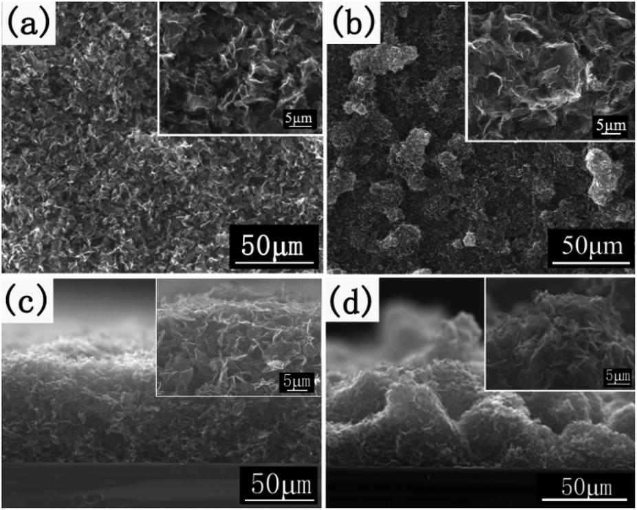 | ||
| Fig. 3 FESEM images of graphene cathodes fabricated by doctor blade method (a) and (c), and by ultrasonic atomization spray method (b) and (d); (a) and (b) are top-view FESEM images, (c) and (d) are cross-section FESEM images. The insets in (a)–(d) are high-magnification FESEM images of the corresponding areas. Both of the samples have a film thickness of about 60 μm. | ||
The substantial improvement of cathode surface morphology over doctor blade coated graphene cathode can be attributed to the unique film construction process of the ultrasonic atomization spray. Under the treatment of ultrasonication atomization, ultrafine solution drops were formed and transported onto silicon substrates by intense spray of compressed nitrogen flow. When the miniaturized graphene-containing droplets was brought into contact with the surfaces heated at 70 °C, a large portion of organic solvents was rapidly removed and the remaining mixture was concentrated in an instant, leading to a transformation of graphene solution from fluid state to semifluid state. As the gradually thickened droplets became much more condensed under the constant heating, they were eventually solidified into micron-scale solid graphene clusters and attached tightly onto silicon substrates. Thus, with the aid of ultrasonic atomization prior to the spray and subsequent continuous heating after the spray, isopropanol-dispersed graphene precursor was transformed from an aqueous solution to a thin and uncontinuous graphene membrane. This uncontinuous graphene membrane was composed of sparse graphene clusters which were formed after the first round of spray. As the coated substrate underwent another round of spray, some of the vacant area during the previous one would be sprayed in this round. Therefore it is very likely that the rest of the bare area of the substrate surface would be filled in next few rounds of spray. As the ultrasonic spray continues, the whole surface of the substrate will be eventually covered with graphene film. In the meanwhile, some of the already coated area would also be overlapped inevitably by this round of spray. For both of the scenarios, an extra layer of graphene was added, tightly attached onto the existing one, thus the thickness of graphene film was increased as long as the number of spraying cycles increased.
Fig. 4 shows the field emission current density versus applied electric field for different graphene cathodes and a pristine Si substrate as reference as well. As can be seen, no emission current was collected for the pristine Si substrate under electric field as high as 5 V μm−1. In this work, the turn-on field (Eto) for graphene field emission cathodes is defined as the applied electric field at which the field emission current density reaches 10 μA cm−2, and the threshold field (Eth) is defined as the applied electric field at which the emission current density reaches 1 mA cm−2. It can be seen that the field emission current density of the 60 μm doctor blade coated graphene cathode rose with increasing electric field. And its Eto and Eth were measured to be 2.23 V μm−1 and 3.76 V μm−1, respectively. At an applied field of 5 V μm−1, an emission current density of 7.27 mA cm−2 was achieved for doctor blade coated graphene cathode. Both of the fair turn-on field and threshold field indicate that a comparative field emission performance can be obtained from the doctor blade coated graphene cathode, which is in accordance with graphene's excellent electrical property and the material's abundant atomic-thin edge emitters. As for the 60 μm graphene cathode coated by ultrasonic atomization spray, the acquired Eto was decreased to 1.85 V μm−1 by 17%, a notable drop from that of the doctor blade coated graphene cathode. In the meanwhile, the corresponding Eth declined to 3.30 V μm−1, 12.2% lower compared with the 60 μm doctor blade coated graphene cathode. As can be seen clearly from the curves in Fig. 4, the field emission current density was significantly enhanced in comparison, and the field emission current density gained at 5 V μm−1 rose sharply up to 14.9 mA cm−2, twice larger than that of the doctor blade coated graphene cathode.
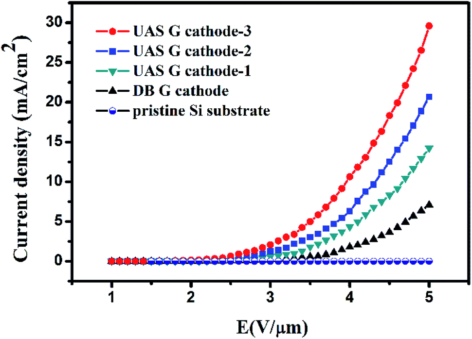 | ||
| Fig. 4 Field emission characteristic curves of current density (J) as a function of applied electric field (E) for pristine Si substrate and four different cathodes: DB G cathode, UAS G cathode-1, UAS G cathode-2, and UAS G cathode-3 have a film thickness of 60 μm, 60 μm, 87 μm, and 116 μm, respectively. | ||
The decreased Eto and Eth along with improved emission current density indicate that, at the same film thickness, the ultrasonic atomizing spray coated graphene cathode notably outperformed the doctor blade coated graphene cathode. The superior field emission performance can be attributed to the roughened surface geometry of the graphene cathode by ultrasonic atomization spray. Through layer-by-layer assembly carried out by the ultrasonic atomizing spray technique, graphene clusters were compactly assembled at the bottom to build up graphene films down from the substrate; while the top of cathode surface comprised numerous graphene clusters, forming a roughened geometrical surface. This is different from the flat surface normally produced by doctor blade technique. On the one hand, the roughened surface geometry feature of the graphene clusters allows more atomic edges to protrude out with ease instead of agglomerating together, giving rise to emergence of abundant graphene edge emitters; on the other hand, the sparsely aligned graphene cluster array reduces the excessively high density of graphene to a large extent, correspondingly resulting in suppressed field-screening effect from over-crowded graphene emitters. It can be drawn that the roughened surface has a beneficial effect on the field emission performance of the ultrasonic atomizing sprayed graphene cathode. Benefiting from the improvement of surface geometry rendered by this unique film construction approach, the ultrasonic atomizing sprayed graphene cathode has more effective edge emitters than the doctor blade coated cathode, and in the meanwhile suffers less from field screening-effect, herein leading to greatly enhanced field emission performance.
The effect of graphene film thickness on ultrasonic atomization spray coated cathodes' filed emission performance was also investigated. As the cathodic film thickness increased to 87 μm, emission current density was elevated to 21.5 mA cm−2 at an electric field of 5 V μm−1, about 44% larger than that of the 60 μm thick graphene cathode coated by the same technique; furthermore, the corresponding Eto and Eth dropped to 1.66 V μm−1 and 2.91 V μm−1 from 1.85 V μm−1 and 3.30 V μm−1, respectively. When the film thickness of ultrasonic atomization spray coated graphene cathodes went up further, the increase of emission current density as well as the decline of both of Eto and Eth was once again observed as above. At the film thickness of 116 μm, the Eto and Eth were determined to be 1.52 V μm−1 and 2.65 V μm−1, respectively, and the emission current density at 5 V μm−1 soared to 29.6 mA cm−2, approximately twice as large as that of the 60 μm ultrasonic atomization spray coated graphene cathode. As can be seen, field emission performance of graphene cathodes by ultrasonic atomizing spray technique is significantly enhanced over doctor blade technique, evidenced by dramatically increased emission current density and sharply decreased Eto and Eth. Another conclusion can be drawn is that as the graphene film thickness increases for the ultrasonic atomizing spray coated cathodes, the emission current density is gradually improved while both Eto and Eth are increasingly lowered in a reverse manner.
It seems that filed emission current density is likely to go up further as long as film thickness increases for the ultrasonic atomization sprayed graphene cathodes. Yet, experiment results show that, as spray time increases furthermore, or when cathodic film reaches a certain thickness, the film quality rapidly deteriorates with emergence of cracks and even exfoliation after sintering treatment. No emission current was collected when cathodic film thickness exceeded 120 μm for all samples.
Current saturation at high fields is often observed for graphene cathodes in many cases. The phenomenon can be ascribed to joule heating, high contact resistance, absorbents on the emitter tip or a large voltage drop along the emitters and/or at the interface of emitter/substrate.18,29 However, due to the limit of measurement, phenomenon of current saturation at high fields wasn't observed for graphene cathodes in this work. Further measurement is needed at higher electric fields to identify existence of current saturation for graphene cathodes fabricated by ultrasonic atomization spray.
As to a field electron emission process, emission behaviour of cathodes should be governed by the Fowler–Nordheim (F–N) equation,

According to the F–N equation, the field enhancement factor β can be expressed as below,

The curves of ln(J/E2) vs. 1/E for different graphene cathodes were plotted in Fig. 5.
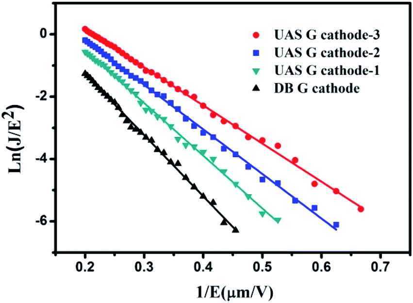 | ||
| Fig. 5 Fowler–Nordheim curves of ln(J/E2) vs. 1/E corresponding to the J–E curves in Fig. 4 for different graphene cathodes. The solid lines represent linear fits to the Fowler–Nordheim equation. | ||
The slopes (kE) were obtained after the F–N curves were linearly fitted, and hence the field emission enhancement factors β can be determined. According to calculation, the emission enhancement factors β for 60 μm doctor blade coated graphene cathode and ultrasonic atomization sprayed graphene cathode were calculated to be 3888 and 4545, respectively. At the same graphene film thickness of 60 μm, the ultrasonic atomization sprayed graphene cathode saw a noticeable reduction in both turn-on field and threshold field but showed a remarkable improvement in field emission current density by over 200% for emission at 5 V μm−1, which is well supported by the greater value of field emission enhancement factor β. The layer-by-layer assembly of micro graphene humps gave rise to the formation of array-alike surface geometry, which allowed more graphene edges to protrude out than the flat film surface to serve as emission tips and hence enabled more electrons to be pulled out under the same electric field; this can also be well explained by the increased β value with regard to improved electron emission. On the other hand, the depressed field-screening effect may also facilitate electron emission for roughened and sparse morphology. Under applied electric field, electron emission process is usually hindered by the field-screening effect, especially for films with a flat and dense morphology. As to the case of layer by layer assembled graphene cathode by ultrasonic atomizing spray, the roughened surface geometry avoided overcrowded density of graphene edges, and to some extent helped to depress the field-screening effect and enhance the electron emission.
The field emission enhancement factors β for 87 μm and 116 μm graphene cathodes were estimated to be 5344 and 6244, respectively. As ultrasonic atomizing spray cycles were repeated, graphene film thickness increased. In the meantime, more micro graphene humps were anchored onto film surface with high probability, leading to increase of emission sites. In addition to the notable decrease of both Eto and Eth when the film thickness increases, emission current density gained at 5 V μm−1 for 116 μm graphene cathode is nearly twice that from 60 μm graphene cathode, which coincides well with the dramatic increase of enhancement factors β. This can be used to explain the large improvement in emission current density for graphene cathodes with larger film thickness.
Turn-on field (Eto) and enhancement factor (β) for different graphene cathodes were showed in Table 1. As can be seen clearly, ultrasonic atomization sprayed graphene cathodes show superior field emission performance over doctor blade coated cathodes; furthermore, as the spray cycles increase, better field emission performance is achieved.
| Sample | Eto | β |
|---|---|---|
| DB G cathode | 2.23 V μm−1 | 3888 |
| UAS G cathode-1 | 1.85 V μm−1 | 4545 |
| UAS G cathode-2 | 1.66 V μm−1 | 5344 |
| UAS G cathode-3 | 1.52 V μm−1 | 6244 |
For cathodes with non-planar structures, local field at the emitting point should be taken into consideration.30 A multistage field enhancement effect can't be neglected, as the local field of the secondary protrusion is enhanced at the primary tip. Therefore, a two-step field enhancement effect can be accounted for enhanced field emission properties. Stratakis et al.29 constructed graphene cathodes with hierarchical structure by utilizing ultrafast lasering structuring and achieved excellent field emission performance. In this work, graphene cathodes fabricated by ultrasonic atomization spray seem to also have a hierarchical structure with cluster-like geometry. However, the aspect ratio (h/r) of graphene cluster is quite low as indicated in Fig. 3(d). A two-step field enhancement effect might contribute to the enhanced field emission performance to some extent, while the increase of sharp emission edges by the roughened geometry and suppressed field-screening effect held greater responsibility for the enhancement of field emission.
In order to examine field emission performance stability for ultrasonic atomization spray coated graphene cathode, stability test was conducted. The graphene cathode tested has a thickness of 100 μm. The test was carried out at an electric field of 1.86 V μm−1 and a starting emission current density of 3.72 mA cm−2 was achieved. After 10 hours of continuous operation under the electric field, a current density of 3.69 mA cm−2 was collected, about 0.8% lower than the initial value. No evident decline or fluctuation of emission current density was observed throughout the operation under such high an emission current density, as shown in Fig. 6. The outcome proves that the graphene cathodes constructed by ultrasonic atomizing spray technique possess a very prominent field emission performance stability. In addition, the emission current density of 3.72 mA cm−2 generated at 1.86 V μm−1 greatly surpasses 1 mA cm−2 which is usually required for practicable field emission applications. The ultrasonic atomization spray technique hereby can be utilized to fabricate high performance field emission devices based on graphene cathodes.
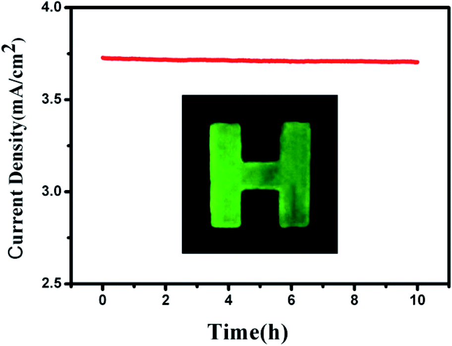 | ||
| Fig. 6 Current density–time curve from field emission stability test for sample UAS-4. Inset: emission pattern for ultrasonic atomization sprayed graphene cathode with a size of ∼8 mm × 10 mm from luminescence test, operated at 1.86 V μm−1. | ||
Ultrasonic atomization spray fabricated graphene cathodes possess low Eto and Eth but high field enhancement and large emission current density compared with results reported by references mentioned in the paper. Due to the variation of definition of Eto and Eth, it's not easy to compare electron emissivity for different cathodes. Nevertheless, graphene cathodes fabricated by ultrasonic atomization spray exhibit large emission current density of ∼30 mA cm−2 and highly stable operation over long hours. In addition, our graphene cathodes seem not to have current saturation at fields as high as 5 V μm−1. The higher the fields are, the larger emission density can be yielded. This advantage is very beneficial for graphene cathodes in applications such as field emission display, electron gun18 and so on.
Green luminescence was observed on the phosphor screen during the field emission luminescence test for the ultrasonic atomization spray coated graphene cathode, as shown in the inset of Fig. 6. The green light sites were uniformly emitted from the capitalized-h shaped area and showed no obvious difference in light luminescence intensity, implying uniform electron emission from graphene cathode. This result also provides strong evidence that ultrasonic atomizing sprayed graphene cathodes can serve as a promising field emitter in field emission displays.7
Conclusions
A novel layer-by-layer assembly strategy was presented to fabricate graphene cathodes by employing an ultrasonic atomization spray method. Herein graphene clusters were used as building blocks for construction of graphene films to yield a roughened cathode surface. The design of array-like geometry greatly increased emission sites and suppressed field-screening effect, which significantly enhanced field emission performance. Compared with doctor blade method, ultrasonic atomization spray endowed graphene films with roughened morphology instead of flat and overpopulated surface, which allows electrons to emit from more sites and more easily. Moreover, turn-on and threshold field were decreased by 17% to 1.85 V μm−1 and by 12% to 3.30 V μm−1 at film thickness of 60 μm. The lowest turn-on and threshold field achieved for 116 μm graphene film were 1.52 V μm−1 and 2.65 V μm−1, respectively. Field emission stability test together with cathode luminescence test demonstrates that ultrasonic atomization sprayed graphene cathodes can be used as a reliable and high-quality electron source. Our results suggest that ultrasonic atomization spray is a feasible and scalable approach towards fabrication of high-performance graphene-based cathodes and holds great promise for large-area field emission applications, such as field emission displays.7,31,32Conflicts of interest
There are no conflicts to declare.Acknowledgements
This work was supported by the National Key Research and Development Program of China (No. 2016YFA0202701), Overseas Expertise Introduction Projects for Discipline Innovation (No. B14003), National Natural Science Foundation of China (No. 51722203, 51672026, 51527802), Beijing Municipal Science & Technology Commission (Z161100002116027).Notes and references
- K. S. Novoselov, A. K. Geim, S. V. Morozov, D. Jiang, Y. Zhang, S. V. Dubonos, I. V. Grigorieva and A. A. Firsov, Science, 2004, 306(5696), 666–669 CrossRef CAS PubMed.
- C. Lee, X. D. Wei, J. W. Kysar and J. Hone, Science, 2008, 321(5887), 385–388 CrossRef CAS PubMed.
- A. K. Geim and K. S. Novoselov, Nat. Mater., 2007, 6(3), 183–191 CrossRef CAS PubMed.
- K. S. Novoselov, A. K. Geim, S. V. Morozov, D. Jiang, M. I. Katsnelson, I. V. Gfigodeva, S. V. Dubonos and A. A. Firsov, Nature, 2005, 438(7065), 197–200 CrossRef CAS PubMed.
- A. A. Balandin, S. Ghosh, W. Z. Bao, I. Calizo, D. Teweldebrhan, F. Miao and C. N. Lau, Nano Lett., 2008, 8(3), 902–907 CrossRef CAS PubMed.
- M. D. Stoller, S. J. Park, Y. W. Zhu, J. H. An and R. S. Ruoff, Nano Lett., 2008, 8, 3498–3502 CrossRef CAS PubMed.
- S. Kumar, G. S. Duesberg, R. Pratap and S. Raghavan, Appl. Phys. Lett., 2014, 105(10), 103107 CrossRef.
- G. Viskadouros, M. M. Stylianakis, E. Kymakis and E. Stratakis, ACS Appl. Mater. Interfaces, 2013, 6(1), 388–393 Search PubMed.
- L. Sygellou, G. Viskadouros, C. Petridis, E. Kymakis, C. Galiotis and D. Tasis, RSC Adv., 2015, 5(66), 53604–53610 RSC.
- X. S. Li, W. W. Cai, J. An, S. Kim, J. Nah, D. X. Yang, R. Piner, A. Velamakanni, I. Jung, E. Tutuc, S. K. Banerjee, L. Colombo and R. S. Ruoff, Science, 2009, 324(5932), 1312–1314 CrossRef CAS PubMed.
- L. L. Jiang, T. Z. Yang, F. Liu, J. Dong, Z. H. Yao, C. M. Shen, S. Z. Deng, N. S. Xu, Y. Q. Liu and H. J. Gao, Adv. Mater., 2013, 25(2), 250 CrossRef CAS PubMed.
- Z. S. Wu, S. F. Pei, W. C. Ren, D. M. Tang, L. B. Gao, B. L. Liu, F. Li, C. Liu and H. M. Cheng, Adv. Mater., 2009, 21(17), 1756–1760 CrossRef CAS.
- V. H. Pham, T. V. Cuong, S. H. Hur, E. W. Shin, J. S. Kim, J. S. Chung and E. J. Kim, Carbon, 2010, 48, 1945–1951 CrossRef CAS.
- J. Z. Xu, R. Pan, Y. W. Chen, X. Q. Piao, M. Qian, T. Feng and Z. Sun, Nanotechnology, 2009, 20(42), 425702 CrossRef PubMed.
- X. Shao, A. Srinivasan, W. K. Ang and A. Khursheed, Nat. Commun., 2018, 9, 1288 CrossRef PubMed.
- L. Chen, H. Yu, J. Zhong, L. Song, J. Wu and W. Su, Mater. Sci. Eng., B, 2017, 220, 44–58 CrossRef CAS.
- G. Viskadouros, D. Konios, E. Kymakis and E. Stratakis, RSC Adv., 2016, 6, 2768–2773 RSC.
- G. Viskadouros, D. Konios, E. Kymakis and E. Stratakis, Appl. Phys. Lett., 2014, 105, 203104 CrossRef.
- E. Stratakis, G. Eda, H. Yamaguchi, E. Kymakis, C. Fotakisa and M. Chhowalla, Nanoscale, 2012, 4, 3069–3074 RSC.
- R. C. Tenent, T. M. Barnes, J. D. Bergeson, A. J. Ferguson, B. To, L. M. Gedvilas, M. J. Heben and J. L. Blackburn, Adv. Mater., 2009, 21(31), 3210–3216 CrossRef CAS.
- H. G. Han, H. C. Weerasinghe, K. M. Kim, J. S. Kim, Y. B. Cheng, D. J. Jones, A. B. Holmes and T. H. Kwon, Sci. Rep., 2015, 5, 14645 CrossRef CAS PubMed.
- L. Petti, H. Faber, N. Münzenrieder, G. Cantarella, P. A. Patsalas, G. Tröster and T. D. Anthopoulos, Appl. Phys. Lett., 2015, 106(9), 092105 CrossRef.
- N. Chantarat, Y. W. Chen, C. C. Lin, M. C. Chiang, Y. C. Chen and S. Y. Chen, J. Phys. Chem. C, 2010, 115(46), 23113–23119 Search PubMed.
- B. Millington, V. Whipple and B. G. Pollet, J. Power Sources, 2011, 196(20), 8500–8508 CrossRef CAS.
- H. Su, T. C. Jao, O. Barron, B. G. Pollet and S. Pasupathi, J. Power Sources, 2014, 267, 155–159 CrossRef CAS.
- Y. Devrim, S. Erkan, N. Baç and I. Eroglu, Int. J. Hydrogen Energy, 2012, 37(21), 16748–16758 CrossRef CAS.
- N. I. Kovtyukhova, P. J. Ollivier, B. R. Martin, T. E. Mallouk, S. A. Chizhik, E. V. Buzaneva and A. D. Gorchinskiy, Chem. Mater., 1999, 11(3), 771–778 CrossRef CAS.
- Z. S. Wu, W. Ren, L. Gao, C. Jiang and H. M. Cheng, Carbon, 2009, 47, 493–499 CrossRef CAS.
- E. Stratakis, R. Giorgi, M. Barberoglou, T. Dikonimos, E. Salernitano, N. Lisi and E. Kymakis, Appl. Phys. Lett., 2010, 96(4), 043110 CrossRef.
- E. Stratakis, Hierarchical Nanostructures for Energy Devices, RSC, Nanoscience & Nanotechnology, 2014, No. 35, p. 230 Search PubMed.
- W. Lei, C. Li, M. T. Cole, K. Qu, S. Y. Ding, Y. Zhang, J. H. Warner, X. B. Zhang, B. P. Wang and W. I. Milne, Carbon, 2013, 56, 255–263 CrossRef CAS.
- C. K. Huang, Y. X. Qu, Y. Q. Bie, Q. Zhao and D. P. Yu, Appl. Phys. Lett., 2011, 98, 263104 CrossRef.
| This journal is © The Royal Society of Chemistry 2018 |