
 Open Access Article
 This Open Access Article is licensed under a Creative Commons Attribution-Non Commercial 3.0 Unported Licence
Fully solution-induced high performance indium oxide thin film transistors with ZrOx high-k gate dielectrics†
Li Zhua,
Gang He *a,
Jianguo Lvb,
Elvira Fortunatoc and
Rodrigo Martinsc
*a,
Jianguo Lvb,
Elvira Fortunatoc and
Rodrigo Martinsc
aSchool of Physics and Materials Science, Radiation Detection Materials & Devices Lab, Anhui University, Hefei 230039, P. R. China. E-mail: hegang@ahu.edu.cn
bDepartment of Physics and Electronic Engineering, Hefei Normal University, Hefei 230061, P. R. China
cDepartment of Materials Science/CENIMAT-I3N, Faculty of Sciences and Technology, New University of Lisbon, CEMOP-UNINOVA, Campus de Caparica 2829-516 Caparica, Portugal
First published on 8th May 2018
Abstract
Solution based deposition has been recently considered as a viable option for low-cost flexible electronics. In this context, research efforts have been increasingly focused on the development of suitable solution-processed materials for oxide based transistors. In this work, we report a fully solution synthesis route, using 2-methoxyethanol as solvent, for the preparation of In2O3 thin films and ZrOx gate dielectrics, as well as the fabrication of In2O3-based TFTs. To verify the possible applications of ZrOx thin films as the gate dielectric in complementary metal oxide semiconductor (CMOS) electronics, fully solution-induced In2O3 TFTs based on ZrO2 dielectrics have been integrated and investigated. The devices, with an optimized annealing temperature of 300 °C, have demonstrated high electrical performance and operational stability at a low voltage of 2 V, including a high μsat of 4.42 cm2 V−1 s−1, low threshold voltage of 0.31 V, threshold voltage shift of 0.15 V under positive bias stress for 7200 s, and large Ion/Ioff of 7.5 × 10⁷, respectively. The as-fabricated In2O3/ZrOx TFTs enable fully solution-derived oxide TFTs for potential application in portable and low-power consumption electronics.
1. Introduction
Metal oxide semiconductors have been attracting considerable attention as excellent channel materials for thin-film transistors (TFTs) in backplane electronics for active-matrix organic light-emitting diodes (AMOLEDs) and other emerging electronic applications such as commentary-metal-oxide-semiconductor (CMOS) and logic gate devices on low cost substrates due to their high mobility, together with high driven currents, the possibility of coupling optical transparency to visible light and mechanical flexibility with excellent electrical performance.1,2 Indeed, the performance of oxide-based TFTs, especially the carrier mobility, exceeds that of amorphous Si-based TFTs, and their stability rivals or exceeds that of typical organic semiconductors.3,4 As a result, metal-oxide-based TFTs have been regarded as the most potential candidates for next generation TFTs in flat panel display driven circuits. Unfortunately, these high-mobility oxide TFTs are conventionally manufactured using costly vacuum-based processing methodologies, such as pulsed laser deposition, atomic layer deposition, and sputtering.1,3 In spite of their advantages from vacuum-based methods, the high fabrication cost and complex preparation process become major obstacles for realizing large-area electronic devices with high performance.In an effort to address this problem, recently, there has been remarkable development of high-performance TFTs based on solution-processable oxide semiconductors, such as spin-coating,5 inkjet printing,6 spray pyrolysis,7 and dip-coating,8 which offers the advantages of simplicity, versatility, and scale-up capability. In addition, solution-derived TFTs have demonstrated impressive performance,9–12 which in some cases are comparable to or even surpass the ones obtained by physical techniques.13 However, for traditional oxide-based TFTs fabricated by solution-processed method, a high temperature annealing process is imperative to obtain optimized semiconductor properties.14 In order to fabricate solution-processed oxide TFTs on flexible polymeric substrates, it is desirable to reduce the process temperature and enable greater process flexibility due to the lower thermal budget. To achieve high performance solution-processed oxide TFTs at low temperatures, appropriate metal precursors, solvents, and gate dielectrics should be taken into account.
As a potential candidate of channel material for the transparent electronics, indium oxide (In2O3) has been paid more attention due to its high electron mobility and high optical transparency in the visible region.15–17 In2O3 exhibits excellent electrical properties, including metallic, semiconducting, and insulating characteristics depending on the stoichiometry and defects in materials.5 Combining the advantages of “solution route” and In2O3 materials, it can be noted that solution-processed In2O3 has been regarded as the promising candidate to fabricate high performance oxide TFTs devices at low temperature.
Although whilst progress on solution-processed oxide TFTs has been rapidly advancing, most of these TFTs generally based on conventional SiO2 as dielectric requires high operation voltages to put out usable drain current.18,19 To decrease operation voltage and power consumption for the realization of mobile and portable applications, recent work has been focused on the investigation of large areal capacitance gate dielectrics, including ultrathin nano-dielectrics,20 electrolyte gate dielectrics,21 and high-k oxide dielectrics.22 Among these candidates, oxide-based high-k dielectrics have been regarded as the promising alternatives due to their high dielectric constant and stable interface chemistry with oxide semiconductors.23,24 By far, oxide transistors based on high-k dielectrics have been confirmed to be successful and demonstrates optimized performance compared to conventional SiO2 dielectrics.7,25–28 Among these, ZrO2 has become one of the most remarkable gate dielectrics due to its relatively high dielectric constants, good thermal stability, and suitable band alignment.16,29 Shan et al. have demonstrated In2O3 TFTs based on ZrOx dielectric exhibits a saturation mobility of 3.08 cm2 V−1 s−1 and an on/off current ratio of 108.16 Pradhan et al. fabricated CdS TFTs with ZrO2 as the gate dielectric grown by chemical bath, which exhibits a low operation voltage of 3.8 V and a field effect mobility of 4 cm2 V−1 s−1.30 Despite their attractive properties, however, TFTs based on high-k gate dielectric are usually realized using stringent and potentially costly manufacturing techniques.7 The development of solution-derived dielectrics is still a step behind, inhibiting the realization of fully solution-processed TFTs with high performance. Although there exist some investigations on the fully solution-processed TFTs, the fabrication of solution-processed TFTs suffers from strict experimental condition, such as high annealing temperature, long annealing time, and complex process, which limits the further development of In2O3 TFTs via the solution route in high performance electronics. Therefore, the experimental process and the device performance of fully solution-derived TFTs should be optimized.
It has been shown that the carrier mobility and transport properties of TFTs, derived from solution-processed methods, are strongly dependent on the preparation condition, including annealing conditions and the precursor solution concentration.15,25,31 However, the annealing temperature modulated electrical properties of the fully solution-processed oxide TFTs is not investigated systematically before. In current work, we demonstrate a fully solution-processed method, a simple and large-area-compatible deposition technique, which can be used for the processing of high-quality ZrO2 dielectric and In2O3 channel layer onto Si substrates. An in-depth investigation was performed to reveal the effect of annealing temperature on the structural and dielectric properties of ZrOx dielectric. In order to confirm the possibility of the In2O3 thin films as channel layer, their applications in TFTs based on ZrOx dielectric by device engineering were also demonstrated. In particular, it has been demonstrated In2O3/ZrOx TFT exhibited a high performance under a ultralow operating voltage of 2 V, with a high Ion/Ioff of around 107, and a high μsat of 4.42 cm2 V−1 s−1.
2. Experimental
2.1 Preparations of precursor solutions
The In2O3 (0.1 M) and ZrOx (0.1 M) precursor solution was synthesized through respectively dissolving indium nitrate hydrate (InN3O9·xH2O) and zirconium oxychloride octahydrate (ZrOCl2·8H2O) in 2-methoxyethanol (C3H8O2) solution. The precursor solutions were stirred at room temperature for 6 h by a magnetic stirrer. After that, to get a more pure sol solution, the solutions were filtered through a 0.22 μm injection filter before spin coating.2.2 Film deposition and devices fabrication
Heavily doped p-type Si wafers with resistivity of 0.02 Ω cm were cleaned by a modified RCA method, and etched by hydrofluoric acid and dried by N2. Then, all-processed wafers were placed in a plasma cleaner to enhance the hydrophilicity of the substrate surface. The ZrOx solution was filtered through a 0.22 μm injection filter and then spun on the hydrophilic Si substrates at 800 rpm for 6 s and 5000 rpm for 25 s, and then ZrOx thin films were placed on the roaster and bake at 150 °C for 10 minutes to remove the residual solvent and cooled to room temperature. In order to obtain the desired thickness, the procedure was repeated twice times. At the end, all the ZrOx thin films were annealed in air with temperatures ranging from 300 °C to 600 °C for 1 h, and their thicknesses were 18.28, 18.02, 17.56, and 17.08 nm, respectively.The In2O3 precursor solution was respectively spun on heavily doped p-type Si substrates with thermally grown SiO2 gate dielectric (200 nm) and 400 °C-annealed ZrOx thin films at 800 rpm for 6 s and 5000 rpm for 25 s, and then the laminated samples were annealed at 250–325 °C in air for 1 h. Finally, Al source and drain electrodes were deposited by thermal evaporation through a shadow mask. The channel length and width for all devices were 100 and 1000 μm, respectively. The detailed schematic diagram of the solution-process for In2O3 and ZrOx thin films and In2O3-based TFTs fabrication are demonstrated in Fig. 1. In order to measure the dielectric properties of the ZrOx thin films, MOS capacitor based on structures of Al/ZrOx/p+-Si/Al were fabricated and investigated using an impedance analyzer (TH2636B).
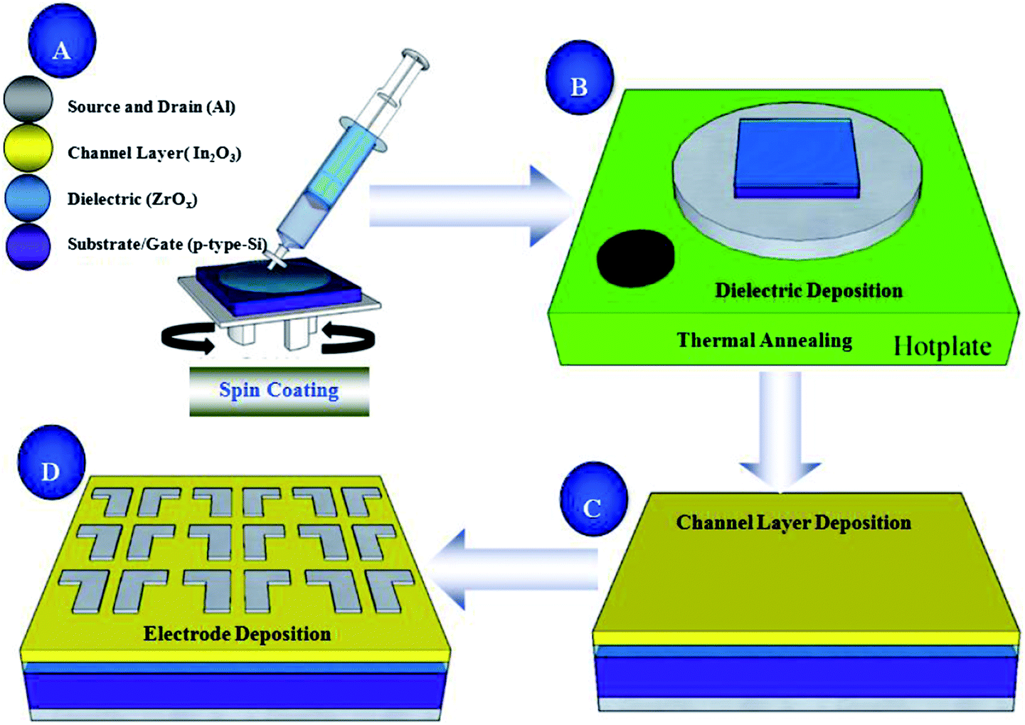 | ||
| Fig. 1 Schematic diagram of solution-derived In2O3 and ZrOx thin films and In2O3 TFTs device fabrication. | ||
2.3 Characterization
The microstructure of ZrOx gate dielectric thin films correlated to annealing temperature were studied by X-Ray diffractometer (XRD). The thickness of In2O3 (about 9 nm) and ZrOx thin films was obtained by spectroscopy ellipsometry (SE) (SC630, SANCO Co, Shanghai). The ultraviolet visible spectroscopy (UV-Vis, Shimadzu, UV-2550) were carried out to investigate the annealing temperature dependent band gap and transmittance spectra of the ZrOx thin films. The surface morphologies of the ZrOx thin films were investigated by atomic force microscopy (AFM). X-Ray photoelectron spectroscopy (XPS, ESCALAB 250Xi Thermo Scientific) was used to analyze the chemical compositions of the ZrOx thin films. The electrical properties of the ZrOx thin films, In2O3/SiO2 TFTs and In2O3/ZrOx TFTs were measured by using an Agilent B1500A semiconductor device analyzer in a dark shelter.3. Results and discussion
3.1 Microstructure and surface morphology of ZrOx thin films
Fig. 2 shows the XRD patterns for the solution-derived ZrOx thin films as a function of annealing temperature. Based on Fig. 2, it can be noted that ZrOx thin films keep amorphous when the annealing temperature is lower than 400 °C. However, when the annealing temperature has increased to 500 °C, the amorphous state disappears and polycrystalline films with diffraction patterns matching that of ZrOx have been detected, indicating that the formation of ZrOx phase is thermally activated and crystallization takes place at 500 °C, which is in good agreement with the observation from Park et al.32 Four main peaks centered at 30.4°, 35.1°, 50.6° and 60.1° corresponding to the (011), (110), (020), and (121) planes of ZrOx, are attributed to the tetragonal phase of ZrO2.32 Further increase of annealing temperature enhances the crystallinity of the film, which is represented by the decreased full width at half maximum (FWHM) of the ZrOx peaks. The high annealing temperature supplies high kinetic energy and increases the surface mobility of deposited particles.31 As we know, as a potential candidate of dielectric layer for TFTs, the amorphous nature of the dielectrics has demonstrates apparent advantage over the crystalline phase due to its low leakage current and high thermal stability. The grain boundaries act as preferential paths for impurity diffusion and leakage current, leading to show high off-state current in TFT devices.33 In addition, dielectric with amorphous structure normally exhibits smooth surface morphology, which is beneficial to obtain dielectric/channel heterointerface with high quality.28 For TFTs, the smooth and sharp interface between channel and dielectric layer is highly desired because carrier transport is generally limited in a narrow region of the interface. Thus, it can be inferred that the annealing temperature for solution-processed ZrOx dielectric should be controlled accurately for the gate dielectric applications. | ||
| Fig. 2 XRD patterns of ZrOx thin films as a function of annealing temperature. | ||
Surface morphology of solution-processed ZrOx dielectric thin films annealed at different temperatures were measured by atomic force microscope (AFM), as shown in Fig. 3. The films roughness was determined from the AFM height profile of a 1 × 1 μm2 area scan. The root mean square (RMS) roughness of ZrOx thin films annealed at 300, 400, 500, and 600 °C are 0.17, 0.37, 0.60, and 0.91 nm, respectively. Based on Fig. 3, RMS values of smaller than 1 nm have been observed for solution-processed ZrOx dielectrics. The smooth surface of the dielectric layer plays an important role in improving the TFT performance and stability. Indeed, the smooth surface is connected to the reduction of the interface charge traps, carrier scattering centers and so, to the production of an excellent interface between the channel layer and the dielectric layer. This will certainly lead to high performance TFTs with higher field-effect mobility and smaller sub-threshold slope (SS) value. Additionally, dielectric with small RMS is also in favor of growing the high-quality channel layer, which is beneficial to obtain high-stability TFTs.34 The slight increase in RMS value for the 600 °C-annealed sample may be attributed to the agglomeration induced by high annealing temperature.
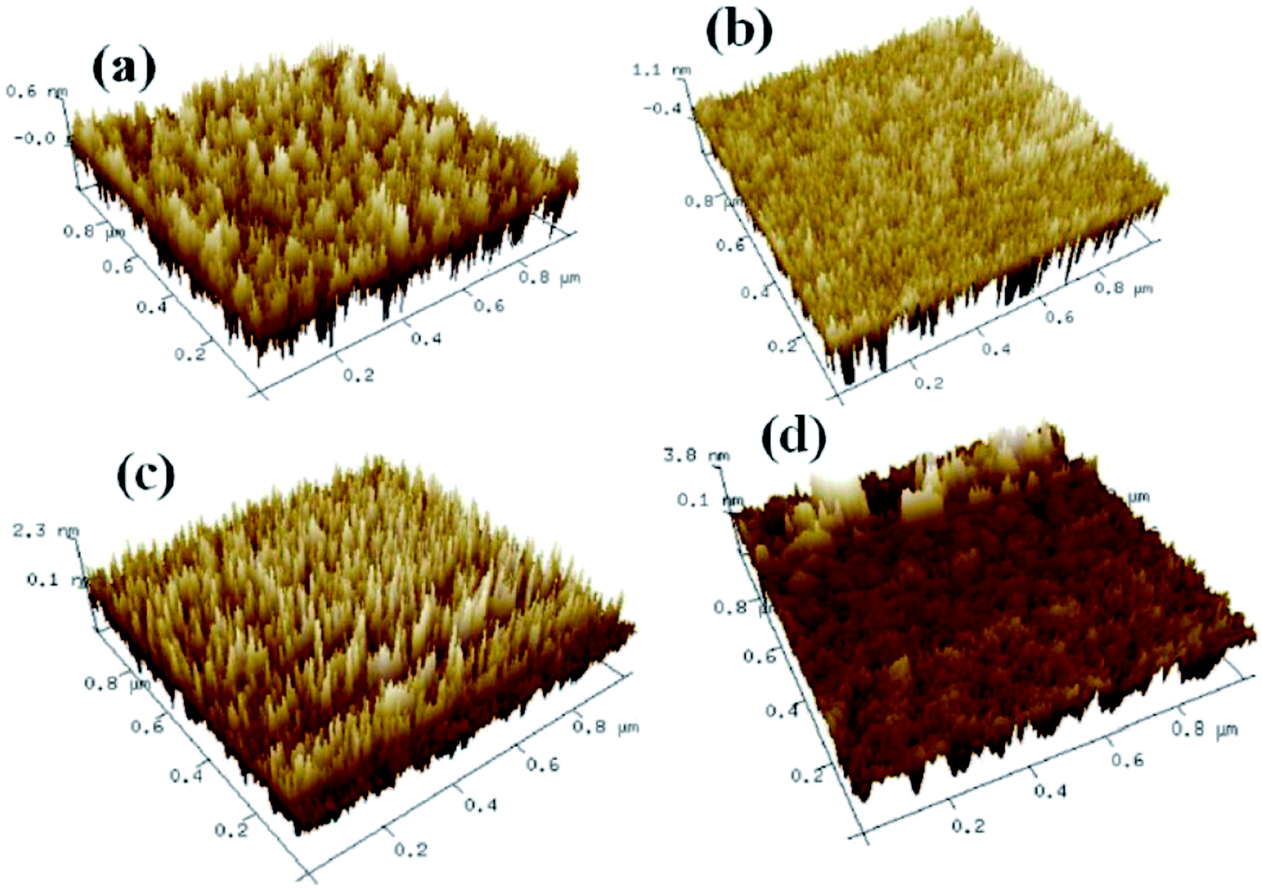 | ||
| Fig. 3 AFM images of the ZrOx thin films annealed at (a) 300 °C, (b) 400 °C, (c) 500 °C, (d) 600 °C. | ||
3.2 Optical properties characterization of ZrOx thin films
To investigate the optical properties of the solution-derived ZrOx dielectric thin films as a function of annealing temperature, the optical transmittances spectra of the ZrOx thin films on quartz substrates were measured with the wavelength ranging from 200 to 900 nm, as demonstrated in Fig. 4. All of the films are highly transparent with an average optical transmittance of over 80% in the visible range. An optical image of the corresponding ZrOx thin films annealed at different temperature is shown as the inset of Fig. 4. No apparent color difference between the bare glass and the samples has been observed, demonstrating the good optical transparency. The high transmittances of the ZrOx thin films indicate the potential applications in transparent electronics. With the increase in annealing temperature, a slight reduction in transmittance has been observed, which can be attributed to the increase in surface roughness of ZrOx thin films or the elimination of oxygen defect at high temperatures.35 The optical band gap of the ZrOx thin films was calculated by using a standard Tauc plotmethod,36 as shown in the inset of Fig. 4. For ZrOx dielectric annealed at low temperature, the presence of defects in thin films would produce localized states in the forbidden gap, which will lead to the reduced band gap energy.26 At high annealing temperature, the annihilation of oxygen vacancies/defects results in the reduced density of localized states and the increased band gap energy. As an candidate of high-k gate dielectric for TFTs, it should process higher packing density and compactness, which can be determined by the optical constant of refractive index. Fig. 5a displays the evolution of refractive index of solution-derived ZrO2 gate dielectrics as a function of annealing temperature. It can be seen that the refractive index increases with the annealing temperature ranging from 300 to 400 °C, indicating the increase in packing density. However, annealing the samples from 500 to 600 °C, reduction in refractive index has been detected, which can be attributed to the increased RMS value for ZrO2 samples. As we know, the refractive index (n) is related to its packing density (p) and its porosity. Based on the following Yoldas formula,| p = (np2 − 1)/(nbulk2 − 1) |
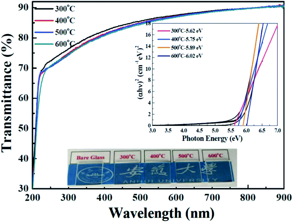 | ||
| Fig. 4 Optical transmittances of ZrOx thin films annealed at different temperatures. The insets above and below display the band gap energy values of these ZrOx films and photographs of bare glass and as-processed ZrOx thin films annealed at various temperatures, respectively. | ||
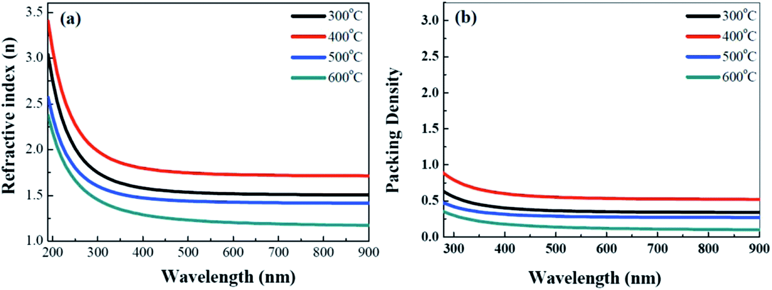 | ||
| Fig. 5 Annealing temperature dependent refractive index (a) and fitting packing density (b) for solution-derived ZrO2 thin films. | ||
3.3 X-Ray photoelectron spectroscopy measurements for ZrOx thin films
The surface impurities, chemical bonding states and compositions of ZrOx thin films were analyzed by X-ray Photoelectron Spectroscopy (XPS). C 1s peak at 284.6 eV was taken as a reference for charge correction. The charge neutralizations of X-ray bombarded samples are performed by flood guns and spectral deconvolution was performed by Shirley background subtraction using a Voigt function convoluting Gaussian and Lorentzian functions. Fig. 6a shows the O 1s core-level XPS spectra for ZrOx thin films as a function of annealing temperature. The deconvoluted O 1s spectra show three peaks centered at 529.8, 531.2, and 532.4 eV, respectively. The peak centers at 529.8 and 531.2 eV can be assigned to the oxygen in oxide lattices (Zr–O) and the oxygen vacancy in lattices (Vo), respectively. The feature at 532.4 eV can originate from the hydroxyl species or absorbed H2O on the surface.17 The semiquantitative analyses of oxygen compositions are summarized in Fig. 6b. The atomic percentages are calculated based on the area integration of each O 1s peak. Based on Fig. 6b, it can be seen that annealing the samples from 300 to 600 °C, the fraction of O2− in ZrOx increases and oxygen vacancy or hydroxyl species decreases, indicating that high temperature annealing removes the bonded oxygen including the oxygen vacancy and hydroxyl species, and improves the metal–oxygen lattice. For a good candidate as dielectric layer, the bonded oxygen in the film should be kept at a relatively low level, which can be explained by the fact that the bonded oxygen generally creates defect states in the forbidden band of dielectric film, contributing the uncontrollable leakage current and the reduced breakdown voltage.37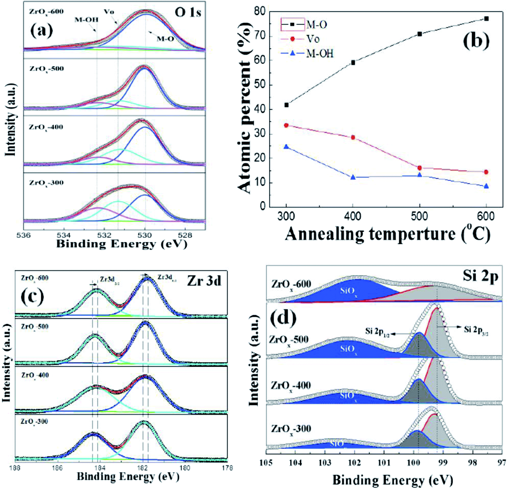 | ||
| Fig. 6 XPS spectra of O 1s (a) and Zr 3d peaks (c) for ZrOx thin films as a function of annealing temperature. (b) Semiquantitative analyses of the oxygen component for the corresponding ZrOx thin films. (d) Si 2p XPS core-level spectra of Si/ZrOx gate stacks annealed at different temperatures. | ||
Fig. 6c displays the XPS Zr 3d core-level spectra of ZrOx dielectric thin films annealed at various temperatures. It can be seen that there is a doublet corresponding to Zr 3d5/2 and Zr 3d3/2 features at 181.8 and 184.1 eV for 300 °C-annealed sample, respectively. With the increase in annealing temperature, the Zr 3d peaks shift to lower binding energies. The same trend has been observed previously in solution-processed ZrOx and ScOx thin films,26,38 which can be due to the full oxidation of ZrOx and the enhanced alloy reaction. To obtain the interface chemistry bonding states and interfacial composition of Si/ZrOx gate stack, XPS depth profile has been performed. After etching the Si/ZrOx gate stack by Ar+, Si 2p has been paid more investigation. Fig. 6d shows the Si 2p core-level XPS spectra as a function of annealing temperature. All Si 2p core-level spectra are fitted with three peaks. For all-processed samples, the fitted substrate doublet peaks (Si–Si) have a separation of 0.57 eV, which is composed of the Si 2p3/2 for 99.27 eV and Si 2p1/2 for 99.84 eV. The third peaks centered at 102–103 eV are attributed to the interfacial SiOx layer. It can be noted that with increasing the annealing temperature, there is a continuous increase in the intensity ratio of the high binding energy content, which is attributed to the formation of more SiOx interfacial layer by diffusion of oxygen from annealing ambient or oxide film.
3.4 Dielectric and electrical properties of ZrOx thin films
In order to investigate the dielectric behavior and electrical properties of solution-grown ZrOx dielectric thin films as a function of annealing temperature, MOS capacitor based on ZrOx/Si gate stack were fabricated. Fig. 7a demonstrates the frequency dependent areal capacitance. Reduction in area capacitance at high frequency has been detected, which can be attributed to the limited polarization response time.17 The areal capacitance of ZrOx thin films annealed at 300, 400, 500, and 600 °C are measured to 388, 313, 268, and 254 nF cm−2 at 103 Hz, respectively. As a result, the relative dielectric constants for all the samples are calculated to be 7.05, 5.69, 5.09, and 4.65, respectively. With the increase in annealing temperature, it can be seen that the areal capacitance demonstrate an apparent decreased trend, which can be attributed to the formation of low-k interface layer,39 which is confirmed by previous XPS measurements. In addition, ZrOx thin films annealed at higher temperatures exhibit weaker frequency dispersion of capacitance, indicating a low defect density such as hydroxyl group and/or oxygen vacancies in thin films. This will be beneficial to control the leakage current because the conduction paths in dielectrics are mainly caused by hydroxyl and grain boundaries.15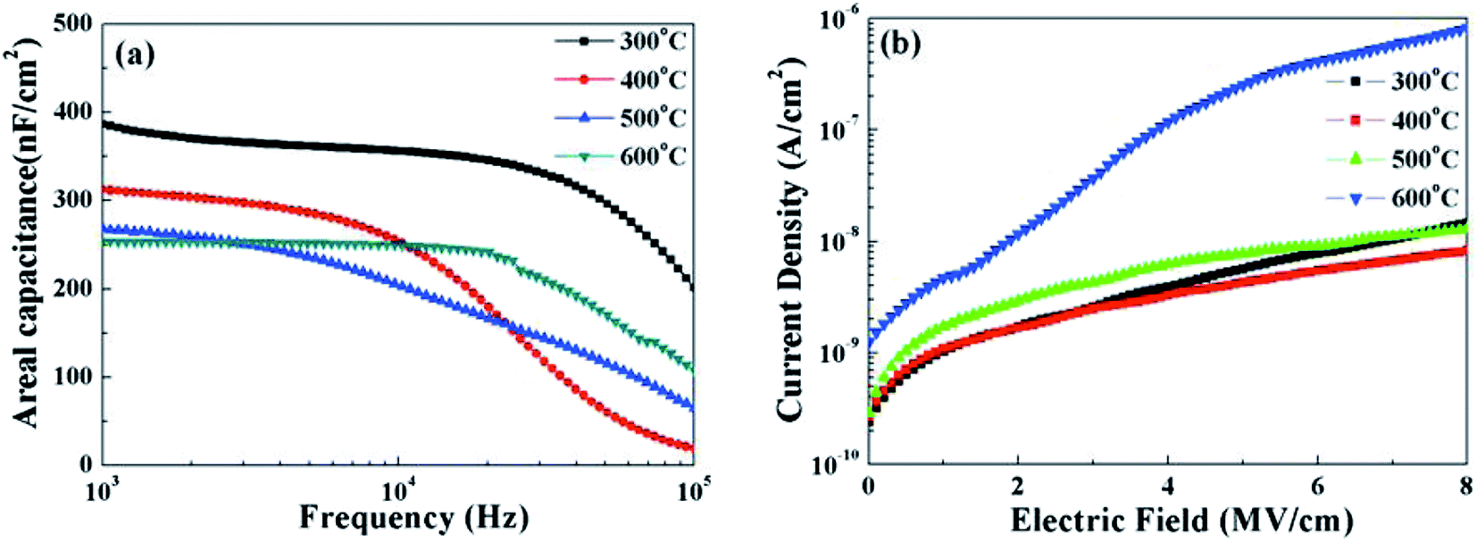 | ||
| Fig. 7 (a) Areal capacitance and (b) leakage current density of the ZrOx dielectric thin films annealed at various temperatures. | ||
The current–density and electric field characteristics of the same ZrOx capacitors are shown in Fig. 7b to evaluate the leakage behavior of the ZrOx thin films. As can be seen, the MOS capacitor devices based on 400 °C-annealed ZrOx dielectrics exhibit a low leakage density of 1.5 × 10⁻⁹ A cm−2 at 2 mV cm−1.40 The decreased leakage current at 400 °C annealing temperature comes from the gradually decomposition of residuals and reduction in the defect density.41 The leakage current density levels for devices annealed at 500 °C and 600 °C have been increased much, originating from the increased surface smooth and the crystallization-induced grain boundaries. As a result, it can be concluded that the sufficient low leakage current for 400 °C-annealed solution-processed ZrOx dielectric attributed to the smooth surface and amorphous structure guarantees its potential application in low-voltage transistor.
3.5 Electrical properties of In2O3 TFTs on SiO2/Si substrate
Based on the aforementioned discussion, it can be inferred that 400 °C-annealed solution-processed ZrOx dielectric can be applied as potential dielectric thin film in TFTs. Before investigating the feasibility of solution-processed ZrOx as gate dielectric in TFTs, the possibility of solution-derived In2O3 TFTs with bottom-gate and top-contact architecture has been evaluated. Thermally-grown SiO2 with thickness of 200 nm is adopted as the dielectric layer due to its low trap defects and high reliability. The schematic diagram of the In2O3 TFTs is displayed in Fig. 8a. The solution-processed In2O3 channel layers were annealed at 250–325 °C. The output curves of each In2O3/SiO2 TFT are shown in Fig. S1 (ESI†) and the typical output characteristics of the as-fabricated In2O3 TFTs annealed at different temperatures, at a gate voltage of (VGS) of 20 V, are depicted in Fig. 8b. It has been found that all the as-fabricated TFTs exhibit typical n-type channel conduction behavior with clear pinch-off voltage and current saturation.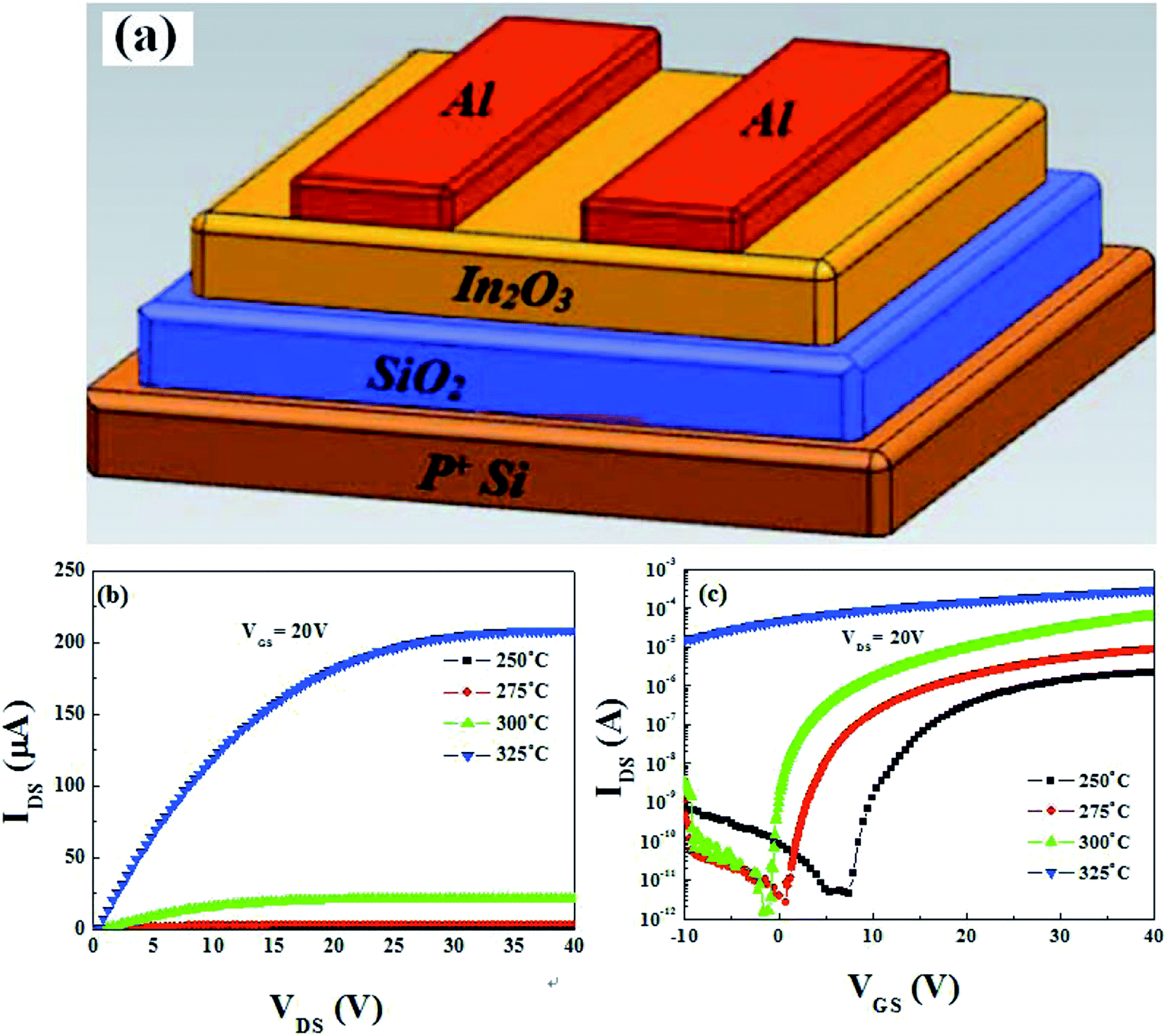 | ||
| Fig. 8 (a) Schematic illustration of the bottom-gate and top-contact In2O3/SiO2 TFTs. (b) and (c) Output and transfer characteristics of the In2O3/SiO2TFTs. | ||
The representative transfer characteristics of In2O3 TFTs as functions of annealing temperatures, at a drain voltage of (VDS) of 20 V, are displayed in Fig. 8c. With increasing the annealing temperature from 250 to 325 °C, the In2O3 TFTs exhibit the increased saturation current and negative shifted threshold voltage (VTH). At the same time, the device operation mode changes from enhancement to depletion mode. The low saturation current at 250 °C may mainly attributed to the formation of defect states and the degree of the oxidation in the channel layer.38 With the formation of high-temperature-induced In–O bonds in In2O3 channel layer and the decreased lattice defects, such as hydroxides and residual impurities,42,43 the improved electrical performance has been achieved at higher annealing temperatures.
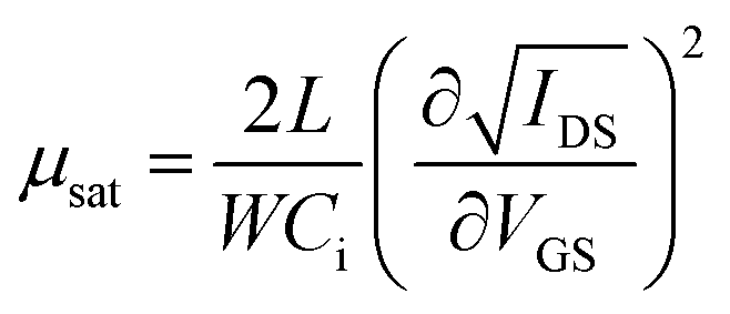
To further investigate the electrical properties of the as-fabricated In2O3 TFTs, the saturation mobility (μsat) and the threshold voltage (VTH) are calculated from the slope of IDS,sat1/2 vs. VGS according to the following equation,16
| Sample | μsat [cm2 V−1 s−1] | Ion/Ioff | VTH [V] | SS [V dec−1] | Dit [cm−2] |
|---|---|---|---|---|---|
| In2O3-250/SiO2 | 0.07 | 4.78 × 10⁵ | 11.25 | 1.09 | 1.35 × 10¹² |
| In2O3-275/SiO2 | 0.13 | 3.30 × 10⁶ | 5.56 | 0.96 | 1.18 × 10¹² |
| In2O3-300/SiO2 | 0.63 | 4.09 × 10⁷ | 4.15 | 0.41 | 4.60 × 10¹¹ |
| In2O3-325/SiO2 | Conductive | 2.12 × 10 | −22.92 | 20.00 | 2.62 × 10¹³ |
The VTH of the In2O3 TFTs based on SiO2 dielectric thin film annealed at 250, 275, 300, and 325 °C is 11.25, 5.56, 4.15, and −22.92 V, respectively. The negative shift of VTH may be mainly due to the decrease amount of interfacial defects acting as carrier trap between In2O3 channel and SiO2 gate dielectric layer. With increasing the annealing temperature, the oxygen vacancy and free carrier concentration decrease. As a result, Ion/Ioff initially increases because of the reduced Ioff. However, further increase of the annealing temperature for In2O3 channel layer to 325 °C leads to the degradation of the device performance, which may be due to the increased trap states near the In2O3/SiO2 interface. The subthreshold swing (SS) value, an important performance parameter, which is defined as the VDS required to increase the IDS by one decade, are calculated to be 1.09, 0.96, 0.41, and 20 V dec−1 in 250, 275, 300, and 325 °C-annealed In2O3 TFTs. A small SS is expected to achieve a high operation speed and low power consumption. Normally, the SS value is dependent on the traps located in channel/dielectric interface.44 Based on SS value, the density of interface states (Dit) can be inferred using the following equation,16
From overall consideration of the electrical performance of the In2O3 TFTs, it can be concluded that the solution-derived In2O3 TFTs annealed at 300 °C exhibits the optimized electrical performance including a high μsat of 0.6 cm2 V−1 s−1, a high Ion/Ioff value of 107, and a small SS value of 0.41 V dec−1, respectively. However, due to the low dielectric constant of SiO2 employed as candidate of gate dielectric in TFTs, all the as-fabricated TFTs devices operate at high voltages and hence increase the power consumption. To decrease the operation voltage and reduce the power consumption of solution-derived In2O3 TFTs, replacing SiO2 with high-k gate dielectric should be explored.
3.6 Electrical properties of solution-processed In2O3/ZrOx TFTs
Encouraged by the successful TFTs performance based on SiO2 dielectric, the TFTs performance needs to be optimized further. To explore the possibility of the improvement of device performance, bottom-gated fully solution-derived TFTs combined with In2O3 channel and ZrOx dielectric layer were fabricated. Based on previous investigation, 400 °C-annealed ZrOx has been selected to act as the dielectric layer due to its relatively low leakage current and good dielectric properties. For the solution-derived In2O3 channel layer, 250–325 °C annealing temperature is still selected to pursue the optimized TFTs device performance.The output curves of each TFT are shown in Fig. S2 (ESI†) and the summarized output curves of In2O3 TFTs at a VGS of 1 V are demonstrated in Fig. 9a. It is noted that an ultra-low operating voltage of 2 V has been observed in ZrOx-based TFTs. Based on our best knowledge, it is the lowest reported operating voltage for fully solution-derived In2O3 TFTs. As a result, the as-fabricated TFTs expend lower consumption compared to those TFTs based on conventional SiO2 dielectrics, which is desirable for low-consumption electronics. Fig. 9b shows the corresponding transfer characteristics of In2O3 TFTs. Table 2 summaries all the electrical parameters of fully solution-derived In2O3 TFTs based on 400 °C-annealed ZrOx dielectrics. It can be clearly seen that In2O3 TFTs annealed at 300 °C represents improved electrical performances, such as a high μsat of 4.42 cm2 V−1 s−1, a low VTH of 0.31 V, an large Ion/Ioff of 7.5 × 10⁷, a turn-on voltage of 0 V, and a small SS of 78.1 mV dec−1. In addition, Dit is calculated to 5.2 × 1011 cm−2 for 300 °C-processed In2O3 TFTs. The as-calculated Dit is much lower than that of the reported TFTs based on solution-derived ZrOx (8.7 × 1011 cm−2),16 sputtered AlOx (1.1 × 1013 cm−2),46 spin-coated MgO (1.1 × 1013 cm−2),17 and water-induced ScOx (1.1 × 1013 cm−2).26 Such a small Dit is not only beneficial to carrier transport in the interface region, but also to the operation stability. The small SS values for 300 °C-annealed TFTs may be attributed to the large areal capacitance of the ZrOx dielectric layer and the electronic-clean interface between In2O3 and ZrOx.15,25 Based on the optimized electrical performance parameters, it can be noted that the μsat of In2O3 TFTs based on ZrOx dielectric has been significantly enhanced by a factor of 7 compared to that of based on SiO2 dielectric. The sharp increase in μsat comes from the electronic-free interface and high capacitance density of ZrOx dielectric layer. According to the multiple-trap-and-release (MTR) model, Lee et al. have supposed that a higher electron mobility may originate from an increased gate capacitance, which stems from the larger dielectric constant of the gate dielectric relative to SiO2.47 The increase in gate capacitance causes electrons to rapidly fill the lower localized states between the energy gap, allowing additional induced electrons to occupy the upper localized states. As a result, electrons can easily jump into the nearby localized states along the percolating-conduction path, leading to the enhanced electron mobility.24 Based on above analyses, it can be concluded that the optimized device performance for 300 °C-annealed In2O3 TFTs based on ZrOx dielectric may be due to the smooth surface, the high capacitance of the ZrOx dielectric, and/or the enhanced interface quality of In2O3/ZrOx.
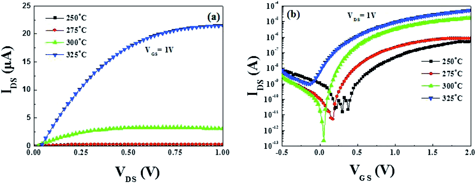 | ||
| Fig. 9 Output and transfer characteristics of the In2O3/ZrOx TFTs. | ||
| Sample | μsat [cm2 V−1 s−1] | Ion/Ioff | VTH [V] | SS [V dec−1] | Dit [cm−2] |
|---|---|---|---|---|---|
| In2O3-250/ZrOx | 0.18 | 2.27 × 10⁴ | 0.56 | 0.11 | 2.13 × 10¹² |
| In2O3-275/ZrOx | 0.32 | 1.61 × 10⁵ | 0.34 | 0.082 | 7.25 × 10¹¹ |
| In2O3-300/ZrOx | 4.42 | 7.50 × 10⁷ | 0.31 | 0.078 | 5.21 × 10¹¹ |
| In2O3-325/ZrOx | 11.32 | 5.50 × 10⁴ | −0.15 | 0.13 | 1.89 × 10¹² |
In spite of the high saturation current and the large μsat for In2O3 TFTs annealed at 325 °C, it operates in the depletion mode with a negative of −0.15 V, which can be due to the high carrier concentration resulting from Fermi level approaching the conduction band minimum (CBM).2 The high carrier concentration, as well as the increased interface defect states make it difficult to deplete In2O3 channel layer, leading to a negative VTH, a high off current, and a low Ion/Ioff. What's more, the corresponding Dit for 325 °C-annealed TFTs is calculated to be 1.89 × 1012 cm−2, approaching nearly one magnitude larger than that of 300 °C-annealed TFTs. The small Ion/Ioff value for 325 °C-annealed TFTs is mainly caused by the large off-state current (Ioff), which will lead to the inevitable static power consumption and degrade device performance.48 It is known that static power consumption is comparable to dynamic power in modern silicon chips or even become dominating in the future.49 Therefore, the Ioff has been regarded as a critical parameter to evaluate the power consumption of a device in modern integrated circuits.
Although solution-derived TFTs based on high-k gate dielectric have been previously achieved, there have been little reports on the investigation of their electrical stability under long-term bias stressing. To investigate the bias stability of the In2O3/ZrOx TFT positive bias stress (PBS) tests were performed by applying a constant gate bias of 1 V while maintaining source and drain electrodes grounded. Fig. 10a displays the transfer curves with stress time intervals for 300 °C-annealed In2O3/ZrOx TFT. The resulting VTH versus stress time has been demonstrated in Fig. 10b. It can be seen that the 300 °C-annealed In2O3/ZrOx TFT exhibits higher operation stability with a small threshold voltage shift (ΔVTH) of 0.15 V up to 7200 s. The negligible change in the SS value reveals that there is no additional defect creation at the channel/dielectric interface during bias stressing.29 The small ΔVTH shift value reveals that there are a small number of defects at the In2O3/ZrOx interface, which is consistent with previous Dit data. Based on the investigation from Jeong et al., it can be noted that the interaction between the channel layer and oxygen from the ambient atmosphere determines the instability.50 Testing PBS in the atmosphere, excess electrons will accumulate in the channel layer. The O2 adsorption in the channel layer can deplete the electron carriers, leading to a positively shift of ΔVTH.29 The chemical reaction and the proposed band diagram are displayed in Fig. 10c.
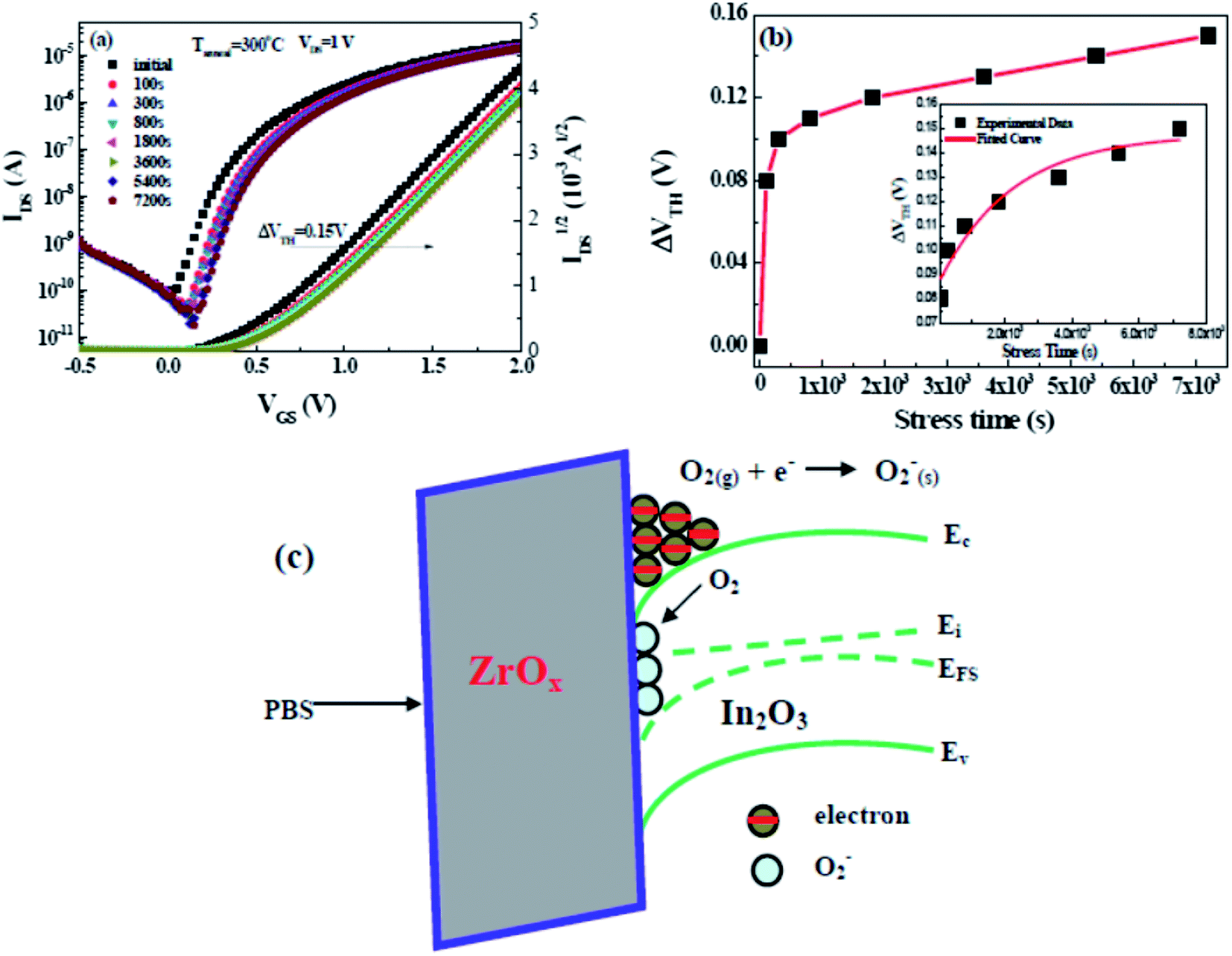 | ||
| Fig. 10 (a) Transfer curves of 300 °C-annealed In2O3/ZrOx TFT under PBS with a VG value of 2 V for 7200 s. (b) The VTH shift as a function of stress time. The inset shows the time dependence of ΔVTH in the In2O3 TFT with an ZrOx gate dielectric under the bias-stress of 1 V. (c) The energy band diagram of the 300 °C-annealed In2O3/ZrOx TFT under PBS. | ||
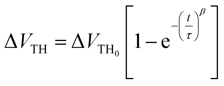
The investigation of the time dependence of ΔVTH can be used to confirm the dominant charge trapping mechanism causing the bias stress-induced ΔVTH in TFTs.51 From the inset plot shown in Fig. 10b, it can be noted that the time dependence of ΔVTH in the In2O3 TFTs device follows a stretched exponential equation. This model is predictive of the voltage threshold shift for long stress durations of up to 2 h. This dependence is indicative of charge trapping phenomenon. The stretched exponential model of ΔVTH is defined as51
The achievement of the high-performance fully solution-derived In2O3 TFTs based on ZrOx gate dielectric indicates the potential application of ZrOx as an excellent high-k dielectric candidate, which represents a significant step towards the development of low-cost, low-power consumption, and large-area oxide flexible electronics. Although the progress made by integrating In2O3 channel layer with high-k gate dielectric, the processing temperature (400 °C) is somewhat beyond the limitation of flexible substrate. In addition, In2O3 and ZrOx in current work has been obtained by conventional solution-based route, the use of toxic organic precursors has hindered its development. An eco-friendly, innovative and green synthetic route should be reconsidered. Currently, water-inducement route15,23 and solution combustion synthesis process53–55 have been adopted to success in reducing the processing temperature. Such process in under way.
4. Conclusions
In summary, we have demonstrated the solution-processed In2O3 thin films and explored its application possibility as channel layer in TFTs. The annealing temperature dependence on the electrical properties of In2O3 TFTs based on SiO2 gate dielectric has been investigated. The optimized In2O3/SiO2 TFTs annealed at 300 °C exhibit excellent electrical performance, including a μsat of 0.6 cm2 V−1 s−1, a high Ion/Ioff value of 107, VTH of 4.15 V, and a small SS value of 0.41 V dec−1, respectively. To verify the possible application of the ZrOx thin films as dielectrics in low-temperature-processed CMOS logics, fully solution-derived In2O3/ZrOx TFTs have been successfully fabricated to display a ultralow operating voltage of 2 V with optimized performance, including a high μsat of 4.42 cm2 V−1 s−1, a low VTH of 0.31 V, an large Ion/Ioff of 7.5 × 10⁷, a small SS of 78.1 mV dec−1, an threshold voltage shift of 0.15 V under positive bias stress for 7200 s, respectively. As a result, it can be inferred that fully solution-based In2O3/ZrOx TFTs have potential application as a promising alternative for low-cost, low-power consumption, and large-area oxide flexible electronics.Conflicts of interest
The authors declare no competing financial interest.Acknowledgements
The authors acknowledge the support from National Natural Science Foundation of China (11774001, 51572002), Technology Foundation for Selected Overseas Chinese Scholar, Ministry of Personnel of China (J05015131), Anhui Provincial Natural Science Foundation (1608085MA06).References
- K. Nomura, H. Ohta, A. Takagi, T. Kamiya, M. Hirano and H. Hosono, Nature, 2004, 432, 488–492 CrossRef CAS PubMed.
- M. Lorenz, M. S. R. Rao, T. Venkatesan, E. Fortunato, P. Barquinha, R. Branquinho, D. Salgueiro, R. Martins, E. Carlos, A. Liu, F. K. Shan, M. Grundmann, H. Boschker, J. Mukherjee, M. Priyadarshini, N. DasGupta, D. J. Rogers, F. H. Teherani, E. V. Sandana, P. Bove, K. Rietwyk, A. Zaban, A. Veziridis, A. Weidenkaff, M. Muralidhar, M. Murakami, S. Abel, J. Fompeyrine, J. Zuniga-Perez, R. Ramesh, N. A. Spaldin, S. Ostanin, V. Borisov, I. Mertig, V. Lazenka, G. Srinivasan, W. Prellier, M. Uchida, M. Kawasaki, R. Pentcheva, P. Gegenwart, F. M. Granozio, J. Fontcuberta and N. Pryds, J. Phys. D: Appl. Phys., 2016, 49, 433001 CrossRef.
- M. Fujii, Y. Ishikawa, R. Ishihara, V. D. C. Johan, M. R. Mofrad, M. Horita and Y. Uraoka, Appl. Phys. Lett., 2013, 102, 122107 CrossRef.
- S. Y. Ju, A. Facchetti, Y. Xuan, J. Liu, F. Ishikawa, P. D. Ye, C. W. Zhou, T. J. Marks and D. B. Janes, Nat. Nanotechnol., 2007, 2, 378–384 CrossRef CAS PubMed.
- S. Y. Han, G. S. Herman and C. H. Chang, J. Am. Chem. Soc., 2011, 133, 5166–5169 CrossRef CAS PubMed.
- D. H. Lee, Y. J. Chang, G. S. Herman and C. H. Chang, Adv. Mater., 2007, 19, 843–847 CrossRef CAS.
- G. Adamopoulos, S. Thomas, P. H. Wöbkenberg, D. D. Bradley, M. A. Mclachlan and T. D. Anthopoulos, Adv. Mater., 2011, 23, 1894–1898 CrossRef CAS PubMed.
- H. Lee, S. M. Dellatore, W. M. Miller and P. B. Messersmith, Science, 2007, 318, 426–430 CrossRef CAS PubMed.
- M. G. Kim, M. G. Kanatzidis, A. Facchetti and T. J. Marks, Nat. Mater., 2011, 10, 382–388 CrossRef CAS PubMed.
- J. W. Hennek, M. G. Kim, M. G. Kanatzidis, A. Facchetti and T. J. Marks, J. Am. Chem. Soc., 2012, 134, 9593–9596 CrossRef CAS PubMed.
- R. M. Pasquarelli, D. S. Ginley and R. O'Hayre, Chem. Soc. Rev., 2011, 40, 5406–5441 RSC.
- C. D. Zhu, G. X. Liu, G. X. Jiang, Y. Meng, E. Fortunato, R. Martins and F. K. Shan, J. Mater. Chem. C, 2016, 4, 10715–10721 RSC.
- E. Fortunato, P. Barquinha and R. Martins, Adv. Mater., 2012, 24, 2945–2986 CrossRef CAS PubMed.
- H. Y. Chong, K. W. Han, Y. S. No and T. W. Kim, Appl. Phys. Lett., 2011, 99, 161908 CrossRef.
- A. Liu, G. X. Liu, H. H. Zhu, F. Xu, E. Fortunato, R. Martins and F. K. Shan, ACS Appl. Mater. Interfaces, 2014, 6, 17364–17369 CAS.
- Y. Meng, G. X. Liu, A. Liu, H. J. Sun, Y. Hou, B. Shin and F. K. Shan, RSC Adv., 2015, 5, 37807–37813 RSC.
- G. X. Jiang, A. Liu, G. X. Liu, C. D. Zhu, Y. Meng, B. Shin, E. Fortunato, R. Martins and F. K. Shan, Appl. Phys. Lett., 2016, 109, 183508 CrossRef.
- Q. Meng, F. J. Zhang, Y. P. Zang, D. Z. Huang, Y. Zou, J. Liu, G. Y. Zhao, Z. R.Wang, D. Y. Ji, C. A. Di, W. P. Hu and D. B. Zhu, J. Mater. Chem. C, 2014, 2, 1264–1269 RSC.
- J. S. Meena, M. C. Chu, Y. C. Chang, H. C. You, R. Singh, P. T. Liu, R. Shieh, P. T. Liu, H. P. D. Shien, F. C. Chang and F. H. Ko, J. Mater. Chem. C, 2013, 1, 6613–6622 RSC.
- M. G. Kim, H. S. Kim, Y. G. Ha, J. Q. He, M. G. Kanatzidis, A. Facchetti and T. J. Marks, J. Am. Chem. Soc., 2010, 132, 10352–10364 CrossRef CAS PubMed.
- H. Liu, J. Sun, Q. Tang and Q. Wan, J. Phys. Chem. C, 2010, 114, 12316–12319 CAS.
- J. Liu, D. B. Buchholz, J. W. Hennek, R. P. H. Chang, A. Facchetti and T. J. Marks, J. Am. Chem. Soc., 2010, 132, 11934–11942 CrossRef CAS PubMed.
- A. Liu, G. X. Liu, H. H. Zhu, B. C. Shin, E. Fortunato, R. Martins and F. K. Shan, J. Mater. Chem. C, 2016, 4, 4478–4484 RSC.
- F. K. Shan, A. Liu, H. H. Zhu, W. J. Kong, J. Q. Liu, B. C. Shin, E. Fortunato, R. Martins and G. X. Liu, J. Mater. Chem. C, 2016, 4, 9438–9444 RSC.
- G. X. Liu, A. Liu, H. H. Zhu, B. C. Shin, E. Fortunato, R. Martins, Y. Q. Wang and F. K. Shan, Adv. Funct. Mater., 2015, 25, 2564–2572 CrossRef CAS.
- A. Liu, G. X. Liu, H. H. Zhu, H. J. Song, B. C. Shin, E. Fortunato, R. Martins and F. K. Shan, Adv. Funct. Mater., 2015, 25, 7180–7188 CrossRef CAS.
- A. Liu, Z. D. Guo, G. X. Liu, C. D. Zhu, H. H. Zhu, B. C. Shin, E. Fortunato, R. Martins and F. K. Shan, Adv. Electron. Mater., 2017, 3, 1600513 CrossRef.
- W. Xu, H. Wang, F. Xie, J. Chen, H. Cao and J. B. Xu, ACS Appl. Mater. Interfaces, 2015, 7, 5803–5810 CAS.
- G. X. Liu, A. Liu, F. K. Shan, Y. Meng, B. C. Shin, E. Fortunato and R. Martins, Appl. Phys. Lett., 2014, 105, 113509 CrossRef.
- H. Dondapati, D. Ha, E. Jenrette, B. Xiao and A. K. Pradhan, Appl. Phys. Lett., 2014, 105, 052105 CrossRef.
- J. M. Yu, G. X. Liu, A. Liu, Y. Meng, B. C. Shin, E. Fortunato and R. Martins, J. Mater. Chem. C, 2015, 3, 9509–9513 RSC.
- J. H. Park, Y. B. Yoo, K. H. Lee, W. S. Jang, J. Y. Oh, S. S. Chae and H. K. Baik, ACS Appl. Mater. Interfaces, 2013, 5, 410–417 CAS.
- P. Barquinha, L. Pereira, G. Goncalves, R. Martins, D. Kuščer, M. Kosec and E. Fortunato, J. Electrochem. Soc., 2009, 156, H824–H831 CrossRef CAS.
- L. Zhang, X. W. Zhang, X. Y. Jiang and Z. L. Zhang, Appl. Phys. Lett., 2009, 95, 072112 CrossRef.
- V. Gupta and A. Mansingh, J. Appl. Phys., 1996, 80, 1063–1073 CrossRef CAS.
- X. G. Yu, L. Zeng, N. Zhou, P. Guo, F. Shi, D. B. Buchholz, Q. Ma, J. Yu, V. P. Dravid, R. P. H. Chang, M. Bedzyk, T. J. Marks and A. Facchetti, Adv. Mater., 2015, 27, 2390–2399 CrossRef CAS PubMed.
- Y. B. Yoo, J. H. Park, K. H. Lee, H. W. Lee, K. M. Song, S. J. Lee and H. K. Baik, J. Mater. Chem. C, 2013, 1, 1651–1658 RSC.
- F. K. Shan, A. Liu, G. X. Liu, Y. Meng, E. Fortunato and R. Martins, J. Disp. Technol., 2015, 11, 541–546 CrossRef CAS.
- S. M. Hwang, S. M. Lee, K. Park, M. S. Lee, J. Joo, J. H. Lim, H. Kim, J. J. Yoon and Y. D. Kim, Appl. Phys. Lett., 2011, 98, 022903 CrossRef.
- B. G. Son, S. Y. Je, H. J. Kim, C. K. Lee, C. K. Lee, A. Y. Hwang, J. Y. Won, J. H. Song, R. Choi and J. K. Jeong, Phys. Status Solidi RRL, 2013, 7, 485–488 CrossRef CAS.
- P. N. Plassmeyer, K. Archila, J. F. Wager and C. J. Page, ACS Appl. Mater. Interfaces, 2015, 7, 1678–1684 CAS.
- J. S. Lee, Y. J. Kwack and W. S. Choi, ACS Appl. Mater. Interfaces, 2013, 5, 11578–11583 CAS.
- S. Jeong, Y. G. Ha, J. Moon, A. Facchetti, T. J. Marks, S. Jeong, Y. G. Ha, J. Moon, A. Facchetti and T. J. Marks, Adv. Mater., 2010, 22, 1346–1350 CrossRef CAS PubMed.
- L. Petti, N. Münzenrieder, C. Vogt, H. Faber, L. Büthe, G. Cantarella, F. Bottacchi, T. D. Anthopoulos and G. Tröster, Appl. Phys. Rev., 2016, 3, 021303 Search PubMed.
- K. Okamura, B. Nasr, R. A. Brand and H. Hahn, J. Mater. Chem., 2012, 22, 4607–4610 RSC.
- J. Li, F. Zhou, H. P. Lin, W. Q. Zhu, J. H. Zhang, X. Y. Jiang and Z. L. Zhang, Curr. Appl. Phys., 2012, 12, 1288–1291 CrossRef.
- E. Lee, J. Ko, K. H. Lim, K. Kim, S. Y. Park, J. M. Myoung and Y. S. Kim, Adv. Funct. Mater., 2014, 24, 4689–4697 CrossRef CAS.
- A. Javey, J. Guo, D. B. Farmer, Q. Wang, E. Yenilmez, R. G. Gordon, M. Lundstrom and H. J. Dai, Nano Lett., 2004, 4, 1319–1322 CrossRef CAS.
- M. L. Geier, P. L. Prabhumirashi, J. J. McMorrow, W. Xu, J. W. Seo, K. Everaerts, T. J. Marks and M. C. Hersam, Nano Lett., 2013, 13, 4810–4814 CrossRef CAS PubMed.
- J. K. Jeong, H. W. Yang, J. H. Jeong, Y. G. Mo and H. D. Kim, Appl. Phys. Lett., 2008, 93, 123508 CrossRef.
- J. M. Lee, I. T. Cho, J. H. Lee, W. S. Cheong, C. S. Hwang and H. I. Kwon, Appl. Phys. Lett., 2009, 94, 222112 CrossRef.
- T. M. Pan, C. H. Chen, J. H. Liu, F. H. Chen, J. L. Her and K. Koyama, IEEE Trans. Electron Devices, 2014, 35, 66–68 CrossRef CAS.
- S. L. Gonzalez-Cortes and F. E. Imbert, Appl. Catal., A, 2013, 452, 117–131 CrossRef CAS.
- Z. Shao, W. Zhou and Z. Zhu, Prog. Mater. Sci., 2012, 57, 804–874 CrossRef CAS.
- X. Yu, J. Smith, N. Zhou, L. Zeng, P. Guo, Y. Xia, A. Alvarez, S. Aghion, H. Lin, J. Yu, R. H. Chang, M. Beddzyk, R. Ferragut, T. Marks and A. Facchetti, Proc. Natl. Acad. Sci. U. S. A., 2015, 112, 3217–3222 CrossRef CAS PubMed.
Footnote |
| † Electronic supplementary information (ESI) available. See DOI: 10.1039/c8ra02108b |
| This journal is © The Royal Society of Chemistry 2018 |