DOI:
10.1039/C8RA01633J
(Paper)
RSC Adv., 2018,
8, 15961-15966
High performance planar p-i-n perovskite solar cells based on a thin Alq3 cathode buffer layer†
Received
24th February 2018
, Accepted 23rd April 2018
First published on 30th April 2018
Abstract
As a thin cathode buffer layer (CBL) tris-(8-hydroxyquinoline), aluminum (Alq3) is successfully introduced into the planar p-i-n perovskite solar cells (PSC) between the PCBM layer and cathode with a device structure of ITO/PEDOT:PSS/CH3NH3PbI3(Cl)/PCBM/Alq3/Ag. Due to the as-introduced thin Alq3 CBL, a high performance planar PSC has been achieved with a fill factor (FF) of 72% and maximum power conversion efficiency (PCE) of 14.22%. The PCE value is approximately 29% higher than that of the reference device without Alq3 CBL. Concerning the results of AC impedance spectra and transient photocurrent measurements, such a remarkable improvement of PCE is mainly attributed to the Alq3-caused better charge-extraction at the cathode, which is induced by reducing charge accumulation between PCBM and Ag.
1. Introduction
Recently, organic–inorganic hybrid perovskite materials have attracted considerable attention due to their strong absorption across the visible spectrum, long carrier diffusion length (100–1000 nm) and low cost of fabrication.1–4 The power conversion efficiency (PCE) of the organometal halide-based perovskite solar cells (PSC) has skyrocketed from 3.8% to 22.1% during the past eight years.5–8 The dramatic improvement of the performance is mainly attributed to the precise control of the fabrication process, the choice of materials and the design of the device architecture.4,9 Up to now, two types of planar architectures are adopted in PSC community: (1) p-i-n structure with transparent conducting oxide (TCO) substrate/hole transport layer(HTL) (p)/perovskite (i)/electron transport layer (ETL) (n);10,11 (2) n-i-p structure with TCO substrate/ETL (n)/perovskite (i)/HTL (p).12,13 Among the two architectures, the n-i-p structure suffers a large hysteresis in the current density–voltage (J–V) characteristics since it consists of an n-type ETL (TiO2, ZnO, etc.).14,15 From this point of view, the p-i-n structure is superior to the n-i-p structure due to its inherent small hysteresis.10,16 In general, solution processable poly(3,4-ethylenedioxythiophene):poly(styrenesulfonate) (PEDOT:PSS) and 6,6-phenyl C61-butyric acid methyl ester (PCBM) are two common used HTL and ETL materials in p-i-n architecture (indium tin oxide (ITO)/PEDOT:PSS/perovskite/PCBM/cathode).17–20 However, due to the band bending and surface states, the direct contact of cathode, e.g. Ag, with PCBM is not an ideal choice for electron extraction. Lately, much attention have been paid on increasing the electron extraction ability at the PCBM/cathode interface to further enhance the performance of PSC.21–23 For example, Xue et al.24 showed that inserting amino-functionalized polymer PN4N between PCBM and cathode could improve the performance of PSC due to the reduction of the contact resistance by suppressing interface charge recombination. BCP and rhodamine have also been served as cathode buffer layers to achieve high PCE in PSC.25–27 Here, the insertion of a BCP or rhodamine CBL could create downward band bending toward the cathode contact to reduce the interface charge recombination, which is helpful for obtaining good ohmic contact. In addition, LiF16,18 and PEIE28 are also commonly used CBL materials, which can create dipole moment across the interfaces to reduce energy barrier between the PCBM and cathode. Apparently, all above mentioned methods highlight the important role of the interface engineering on electron extraction ability at the PCBM/cathode interface to further enhance the performance of PSC. However, some of these CBLs show relatively unstable properties, such as the crystallization of BCP in air at room temperature.29 Although heavily n-doped (n+) TiOx was recently developed as stable CBL to extract electrons efficiently,30 developing new stable CBLs with easy and precise controllability has been taken into account. Alternatively, tris-(8-hydroxyquinoline) aluminum (Alq3) is another small molecular organic material, which can be thermal deposited to form a more stable and uniform thin layer.29 Thus, it is probably to use Alq3 as a potential CBL in PSC.
In this work, a thin Alq3 CBL has been inserted into the PCBM/cathode interface with a planar configuration of ITO/PEDOT:PSS/CH3NH3PbI3(Cl)/PCBM/Alq3(1.5 nm)/Ag. A maximum PCE (14.22%) and FF (72%) were achieved in the device with Alq3 CBL, which is ∼29% and ∼20% higher than that of PSC without Alq3 CBL (PCE of 11.04% and FF of 60%). Such improvements can be attributed to the high efficiency charge-extraction, which was solidly confirmed by the reduction of charge transfer resistance from AC impedance spectrum measurement and fast charge-extraction from transient photocurrent measurement.
2. Experimental section
2.1 Materials
PEDOT:PSS (Clevios PVP Al 4083), methylammonium iodide (MAI, 99.5%), PbCl2 (99.99%), PbI2 (99.99%), PCBM (99%) were purchased form Xi'an Polymer Light Technology Corp (China), while N,N-dimethylformamide (DMF, 99.8%), dimethyl sulfoxide (DMSO, 99.9%), chlorobenzene (CB, 99.8%) and Alq3 (99.995%) were purchased from Sigma-Aldrich. A solution of 0.14 M PbCl2, 1.26 M PbI2 and 1.4 M MAI in a cosolvent of DMSO and DMF (vol. ratio = 1![[thin space (1/6-em)]](https://www.rsc.org/images/entities/char_2009.gif) :9) was prepared in a glove box and stirred overnight under room temperature. 15 mg PCBM was dissolved in 1 mL CB and stirred overnight under room temperature.
:9) was prepared in a glove box and stirred overnight under room temperature. 15 mg PCBM was dissolved in 1 mL CB and stirred overnight under room temperature.
2.2 Device fabrication
ITO was cleaned by an ultrasonic cleaning machine (KQ3200DV) with 4% detergent (Decon 90) sequentially in deionized water and ethanol at 60 °C. PEDOT:PSS was spin-coated on ITO at 6000 rpm for 60 s in air and dried on hotplate at 120 °C for 20 min. Then the perovskite precursor solution was spin-coated on the PEDOT:PSS at 1000 rpm for 3 s and 4000 rpm for 20 s. When the perovskite precursor was roll out for 10 s, chlorobenzene (200 μL) was dropwise added onto the 4000 rpm spinning film. The film was heated at 60 °C for 2 min and then 85 °C for 25 min on a hotplate. The PCBM was spin-coated on the perovskite film from chlorobenzene solution (15 mg mL−1) with a speed of 4000 rpm for 40 s. All the above procedures were conducted inside a N2-filled glovebox with oxygen and moisture levels <3 ppm except for casting the PEDOT:PSS in ambient air. Finally, 1.5 nm Alq3 and 100 nm Ag were deposited under high-vacuum (∼5 × 10⁻⁵ Pa) through a shadow mask, resulting in an active area of 0.09 cm2. The film thickness was monitored in situ by a quartz crystal.
2.3 Characterization
The crystal structures of the perovskite were investigated by an X-ray diffraction system (Shimadzu XRD-7000). The grain size of the perovskite structure was characterized by field-emission scanning electron microscopy (SEM, JSM-6700F). UV-vis absorption spectra measurements were carried out using Shimadzu UV-2550 spectrometer. The J–V characteristics were measured by a Keithley 2400 source meter with 100 mW cm−2 (AM 1.5G) simulated light from a Newport simulator (model 94043A). During the measurement, the scan direction was reverse (from +1.2 to −1.2 V) or forward (from −1.2 to +1.2 V) with a voltage step of 10 mV and 0 ms delay time by Keithley 2400. The external quantum efficiency (EQE) of devices was calculated from photocurrent generated from the modulated monochromatic light which was measured by a lock-in amplifier (SR-830). The J–V and EQE characteristics were measured in nitrogen filled glove box with less than 3 ppm of H2O and O2. The alternating-current (AC) impedance spectrum measurement was performed on an electrochemical workstation (model 660D, Shanghai Chenhua Instrument Co., Ltd., China) in dark, with an applied bias of Voc (1.01 V). An AC signal with an amplitude of 10 mV over the frequency range of 1 MHz to 1 Hz was adopted. The impedance parameters were determined by fitting the impedance spectra using Z-view software. In transient photocurrent (TPC) characteristics, the PSC were connected directly in series with an oscilloscope (Agilent DSO-X3102A) and the input impedance of the oscilloscope is switched to 50 ohms. All the voltages were relative to the Ag electrode.
3. Results and discussion
3.1 Photovoltaic performance of PSC
Schematic structure of the planar p-i-n PSCs with Alq3 CBL and its corresponding energy level2,31 are shown in Fig. 1(a) and (b), respectively.
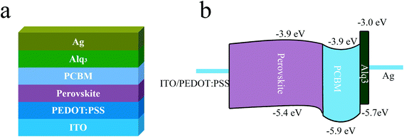 |
| | Fig. 1 (a) Schematic structure of the PSC with Alq3 CBL. (b) The corresponding energy level diagram of the PSC. | |
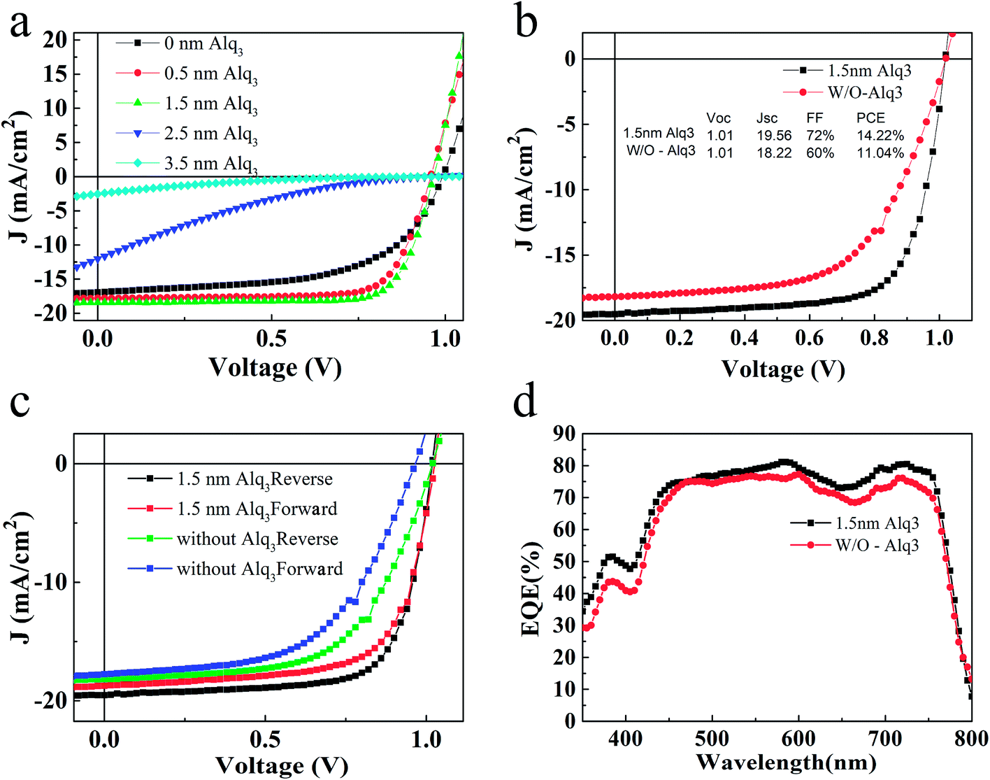
The J–V characteristics of the devices with different thickness (0, 0.5, 1.5, 2.5, 3.5 nm) of Alq3 CBL are shown in Fig. 2(a), and their corresponding photovoltaic parameters are listed in Table 1. It is found that the PCE of PSC increases with the increase of Alq3 thickness until1.5 nm and then decreases with further increasing Alq3 thickness. The J–V characteristics of the best devices are shown in Fig. 2(b). The PSC without Alq3 CBL exhibits an open circuit voltage (Voc), a short current density (Jsc), FF and PCE of 1.01 V, 18.22 mA cm−2, 60% and 11.04%, respectively. After inserting 1.5 nm Alq3 CBL between PCBM and Ag interface, the highest FF and Jsc increase to 72% and 19.56 mA cm−2, respectively. As a consequence, the PCE increases to 14.22%. To confirm the accuracy of Jsc, the EQE spectra of the devices were measured and display in Fig. 2(d). The integrated current densities of the devices with 1.5 nm Alq3 and without Alq3 CBL are 18.97 mA cm−2 and 17.97 mA cm−2, respectively, agreeing with the previous J–V curves results. In addition, the similar shape of the EQE spectra indicate the Alq3 was too thin to alter the spatial distribution of the optical field in the device, which are consistent with the similar absorbance of perovskite films with and without Alq3 (Fig. S3†). As the existence of Alq3 varies the two devices, the characteristics of device interface should be the reason of a different performance in the Alq3 CBL PSC: a reduced interface resistance may improve the performance. Thereafter, the series resistance (Rs) was calculated from the slope of J–V curves at 0 mA cm−2, as listed in Table 1. Compared with the Rs extracted from the PSC without Alq3 CBL (7.24 Ω cm2), the notable reduction of Rs with 1.5 nm Alq3 CBL (2.52 Ω cm2) can reasonably explain the improvement of Jsc and FF. Fig. 2(c) shows the forward (from −1.2 to +1.2 V) and reverse (from +1.2 to −1.2 V) J–V characteristics of PSCs with 1.5 nm Alq3 CBL and without Alq3 CBL, respectively. The hysteresis is obviously reduced in the device with 1.5 nm Alq3 CBL, suggesting less surface traps formation at the Alq3/Ag interface and then highlights the role of the Alq3 CBL. And the J–V hysteresis curves under an illumination of AM 1.5G, 100 mW cm−2 at different delay time are presented in ESI Fig. S4.†
 |
| | Fig. 2 (a) J–V curves of PSCs with different thickness (0, 0.5, 1.5, 2.5, 3.5 nm) of Alq3 CBL under an illumination of AM 1.5G, 100 mW cm−2. (b) J–V curves of best devices with 1.5 nm Alq3 and without Alq3 CBL. (c) The forward and reverse J–V curves under an illumination of AM 1.5G, 100 mW cm−2 for PSC devices. (d) EQE spectra for PSC with 1.5 nm Alq3 and without Alq3 CBL. | |
Table 1 Photovoltaic performance of p-i-n PSC with different thickness Alq3 and without Alq3 CBL
| CBL |
Voc (V) |
Jsc (mA cm−2) |
FF (%) |
PCE (%) |
Rs |
| 0 nm Alq3 |
0.99 |
16.08 |
58 |
9.23 |
9.73 |
| 0.5 nm Alq3 |
0.99 |
16.88 |
76 |
12.15 |
8.77 |
| 1.5 nm Alq3 |
0.97 |
17.05 |
77 |
13.06 |
6.08 |
| 2.5 nm Alq3 |
0.95 |
10.15 |
17 |
1.60 |
292.26 |
| 3.5 nm Alq3 |
0.95 |
5.39 |
14 |
0.71 |
1854.21 |
| 1.5 nm Alq3 (best) |
1.01 |
19.56 |
72 |
14.22 |
2.52 |
| Without Alq3 (best) |
1.01 |
18.22 |
60 |
11.04 |
7.24 |
The most obvious effect of adding Alq3 CBL on the device performance is the enhancement of FF and Jsc in the p-i-n PSC, similar to the results by using other CBLs.16,26 This effect thus can be similarly explained as the result of suppressing upward band bending of PCBM, reducing the interfacial charge recombination to achieve a better electron extraction from PCBM. Fig. 3 exhibits schematic band diagrams of the cells under light illumination. Owing to the mismatch of the Fermi level of PCBM and the work function of the metal cathode, a Schottky barrier and then a reverse electrical field in PCBM are created in the device without Alq3 CBL. Because of the Schottky barrier, electrons from the perovskite accumulate in PCBM, leading to charge recombination with holes in perovskite, as shown in Fig. 3(a). The insertion of a thin Alq3 CBL shifts down the band bending to the cathode contact in the PCBM layer (Fig. 3(b)), which is beneficial to electron transportation. Meanwhile, the inserted Alq3 CBL is thin enough for photo-induced electrons tunneling across the PCBM/cathode interface. Therefore, charge accumulation seldomly emerges at the PCBM/Alq3/Ag interface. The reduction of Rs after adding a thin Alq3 layer are observed in Table 1. When the thickness of Alq3 was further increased over 1.5 nm, it would block the electron transportation due to the rapidly increased Rs.
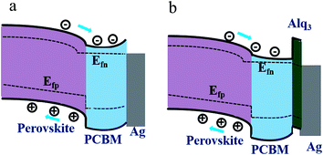 |
| | Fig. 3 Schematic band diagrams under light illumination for the PSCs without and with Alq3 CBL. (a) perovskite/PCBM/Ag and (b) perovskite/PCBM/Alq3/Ag. | |
3.2 Alternating-current impedance spectrum measurement
To further explore the effect of adding Alq3 CBL on electrical properties, the AC impedance spectrum measurement was performed on the two devices with 1.5 nm Alq3 and without Alq3 CBL in the dark at near the Voc (1.01 V). The Nyquist plots of the two PSC are shown in Fig. 4(a). The semicircle of the PSC with 1.5 nm Alq3 CBL shrinks to a smaller one compared with the device without Alq3 CBL. These AC impedances can be well fitted by an equivalent electrical circuit, as shown in Fig. 4(b). The equivalent electrical circuit is composed of three serial connected parts:32 (1) an ohmic series resistance (Ros) related to the electrical contacts, and sheet resistance of collecting electrodes; (2) a RC circuit (R1C1) describing the property of interface between the active layer and electrodes; (3) another RC circuit (R2C2) describing the behavior of photoactive layer. The fitting parameters are summarized in Table 2. A little difference of the Ros between the two cells are observed, which could be attributed to the similar configuration. Especially, the value of R1 extracted from the devices with and without Alq3 CBL are respectively 39 and 174 Ω. The obvious reduction of R1 in the Alq3 CBL is consistent with the Rs obtained from J–V curves and confirms a better charge transfer between the PCBM and Ag electrodes.
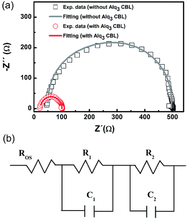 |
| | Fig. 4 (a) Nyquist plots and fitting curves (solid line) of PSCs without (black square) and with (red circle) 1.5 nm Alq3 CBL. AC impedance was measured in the dark at near the Voc. (b) Equivalent electrical circuit used for fitting the impedance data. | |
Table 2 Parameters of equivalent circuit for the p-i-n PSCs with 1.5 nm Alq3 CBL and without Alq3 CBL
| CBL |
Ros (Ω) |
R1 (Ω) |
C1 (F) |
R2 (Ω) |
C2 (F) |
| 1.5 nm Alq3 |
23 |
39 |
3.03 × 10⁻⁸ |
39 |
3.03 × 10⁻⁸ |
| Without Alq3 |
48 |
174 |
8.33 × 10⁻⁹ |
265 |
1.67 × 10⁻⁸ |
3.3 TPC measurements of PSC
To assess the practical benefits of the reduced interface resistance, we examined the charge-extraction time of the two PSC via transient photocurrent (TPC) analyses. The charge-extraction time can be extracted from the TPC response to accurately describe the efficiency of charge-extraction.33 Fig. 5 displays the normalized TPC in the PSC with 1.5 nm Alq3 and without Alq3 CBL. The PSC with 1.5 nm Alq3 CBL shows a shorter charge-extraction time (0.51 μs), indicating that there is an efficient charge-extraction in the Alq3 CBL device compared with that without Alq3 CBL (0.67 μs). Thus, the better contact interface (due to reduced interface resistance) and the reduced surface traps (reflects in reduced hysteresis) contribute together to gain the high efficient charge-extraction in the device with 1.5 nm Alq3 CBL. These results have no doubt provided strong and unequivocal support to our speculation that Alq3 CBL leads to high efficient charge-extraction at the cathode interface and then the high FF, and Jsc.
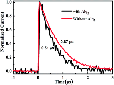 |
| | Fig. 5 TPC measurements of PSCs with and without Alq3 CBL. | |
Compared with state of the art planar perovskite solar cells, the relative low performance in this study is due to relative low Voc and Jsc. The higher Voc can be achieved to choose better ETL/HTL. The low Jsc might be partially due to the unoptimized thickness of active perovskite film to generate charge carrier. The thickness of active perovskite film measured by step profiler in this study is about 350 nm, which means that some incident light is not absorbed by the perovskite film, as shown in Fig. S3.† Another reason for this low Jsc is the charge recombination in the perovskite film and at the perovskite/ETL(HTL) interface, which has been improved in this study. Thus, by further optimizing the perovskite film and choosing better pair of ETL/HTL, the performance of planar perovskite solar cells can be hopefully improved in the future work.
4. Conclusion
In summary, we demonstrated an enhancement of Jsc, FF and PCE in p-i-n PSCs by inserting a thin Alq3 CBL between PCBM and Ag electrode. Due to the existence of 1.5 nm Alq3 CBL, the PSC with a Jsc of 19.56 mA cm−2, a FF of 72% and a PCE of 14.22% was achieved. In comparison, the PSC without Alq3 CBL only show a Jsc of 18.22 mA cm−2, a FF of 60% and a PCE of 11.04%. The remarkable improvement of performance is attributed to the efficient charge-extraction due to the reduction of charge accumulation and contact resistance at the cathode interface, which is confirmed by comparing AC impedance and TPC results between the two PSC. We believe that inserting a thin Alq3 CBL provides a promising strategy to achieve high performance of p-i-n planar perovskite solar cells.
Conflicts of interest
There are no conflicts to declare.
Acknowledgements
This work was supported by the National Natural Science Foundation of China (Grant No. 11274256, 11774293, 11504036), Program for Innovation Team Building at Institutions of Higher Education in Chongqing (Grant No. CXTDX201601011), Scientific and Technological Research Program of Chongqing Municipal Education Commission (Grant No. KJ1500318 and KJ1600327), The Natural Science Foundation Project of CQ CSTC (Grant No. CSTC2017jcyjAX0333 and CSTC2015jcyjBX0032) and Fundamental Research Funds for the Central Universities (Grant No. XDJK2017A002).
References
- G. Xing, N. Mathews, S. Sun, S. S. Lim, Y. M. Lam, M. Grätzel, S. Mhaisalkar and T. C. Sum, Science, 2013, 34, 344 CrossRef PubMed.
- G. Zhou, J. Wu, Y. Zhao, Y. Li, J. Shi, Y. Li, H. Wu, D. Li, Y. Luo and Q. Meng, ACS Appl. Mater. Interfaces, 2018, 10, 9503 CAS.
- S. D. Stranks, G. E. Eperon, G. Grancini, C. Menelaou, M. J. Alcocer, T. Leijtens, L. M. Herz, A. Petrozza and H. J. Snaith, Science, 2013, 342, 341 CrossRef CAS PubMed.
- J. Zheng, M. Zhang, C. F. J. Lau, X. Deng, J. Kim, Q. Ma, C. Chen, M. A. Green, S. Huang and A. W. Y. Ho-Baillie, Sol. Energy Mater. Sol. Cells, 2017, 168, 165 CrossRef CAS.
- A. Kojima, K. Teshima, Y. Shirai and T. Miyasaka, J. Am. Chem. Soc., 2009, 131, 6050 CrossRef CAS PubMed.
- M. Saliba, T. Matsui, K. Domanski, J. Y. Seo, A. Ummadisingu, S. M. Zakeeruddin, J. P. Correa-Baena, W. R. Tress, A. Abate and A. Hagfeldt, Science, 2016, 354, 206 CrossRef CAS PubMed.
- Y. Q. Yao, G. Wang, F. Wu, D. B. Liu, C. Y. Lin, X. Rao, R. Wu, G. D. Zhou and Q. L. Song, RSC Adv., 2017, 7, 42973 RSC.
- Z. Hu, J. Miao, T. Li, M. Liu, I. Murtaza and H. Meng, Nano Energy, 2018, 43, 72 CrossRef CAS.
- D. B. Liu, G. Wang, F. Wu, R. Wu, T. Chen, B. F. Ding and Q. L. Song, Org. Electron., 2017, 43, 189 CrossRef CAS.
- D. Forgács, M. Sessolo and H. J. Bolink, J. Mater. Chem. A, 2015, 3, 14121 Search PubMed.
- J. Miao, Z. Hu, M. Liu, M. U. Ali, O. Goto, W. Lu, T. Yang, Y. Liang and H. Meng, Org. Electron., 2018, 52, 200 CrossRef CAS.
- M. Liu, M. B. Johnston and H. J. Snaith, Nature, 2013, 501, 395 CrossRef CAS PubMed.
- X. Zheng, H. Lei, G. Yang, W. Ke, Z. Chen, C. Chen, J. Ma, Q. Guo, F. Yao, Q. Zhang, H. Xu and G. Fang, Nano Energy, 2017, 38, 1 CrossRef CAS.
- M. Shahiduzzaman, M. Karakawa, K. Yamamoto, T. Kusumi, K. Yonezawa, T. Kuwabara, K. Takahashi and T. Taima, Sol. Energy Mater. Sol. Cells, 2018, 178, 1 CrossRef CAS.
- J. Cao, B. Wu, R. Chen, Y. Wu, Y. Hui, B.-W. Mao and N. Zheng, Adv. Mater., 2018, 30 Search PubMed.
- X. Liu, H. Yu, L. Yan, Q. Dong, Q. Wan, Y. Zhou, B. Song and Y. Li, ACS Appl. Mater. Interfaces, 2015, 7, 6230 CAS.
- S. Cong, H. Yang, Y. Lou, L. Han, Q. Yi, H. Wang, Y. Sun and G. Zou, ACS Appl. Mater. Interfaces, 2017, 9, 2295 CAS.
- J. Seo, S. Park, Y. C. Kim, N. J. Jeon, J. H. Noh, S. C. Yoon and S. I. Seok, Energy Environ. Sci., 2014, 7, 2642 CAS.
- H. Yoon, S. M. Kang, J. K. Lee and M. Choi, Energy Environ. Sci., 2016, 9, 2262 CAS.
- W. K. Lin, S. H. Su, M. C. Yeh, C. Y. Chen and M. Yokoyama, Vacuum, 2017, 140, 82 CrossRef CAS.
- Q. Wang, Y. Shao, Q. Dong, Z. Xiao, Y. Yuan and J. Huang, Energy Environ. Sci., 2014, 7, 2359 CAS.
- G. Wang, D. B. Liu, J. Xiang, D. C. Zhou, K. Alameh, B. F. Ding and Q. L. Song, RSC Adv., 2016, 6, 43299 RSC.
- C. Li, F. Wang, J. Xu, J. Yao, B. Zhang, C. Zhang, M. Xiao, S. Dai, Y. Li and Z. Tan, Nanoscale, 2015, 7, 9771 RSC.
- Q. Xue, Z. Hu, J. Liu, J. Lin, C. Sun, Z. Chen, C. Duan, J. Wang, C. Liao and W. M. Lau, J. Mater. Chem. A, 2014, 2, 19598 CAS.
- C. Chen, S. Zhang, S. Wu, W. Zhang, H. Zhu, Z. Xiong, Y. Zhang and W. Chen, RSC Adv., 2017, 7, 35819 RSC.
- J. Liu, G. Wang, K. Luo, X. He, Q. Ye, C. Liao and J. Mei, ChemPhysChem, 2017, 18, 617–625 CrossRef CAS PubMed.
- J. Ciro, S. Mesa, J. I. Uribe, M. A. M. Escobar, D. Ramirez, J. F. Montoya, R. Betancur, H. S. Yoo, N. G. Park and F. Jaramillo, Nanoscale, 2017, 9, 9440 RSC.
- H. Zhang, H. Azimi, Y. Hou, T. Ameri, T. Przybilla, E. Spiecker, M. Kraft, U. Scherf and C. J. Brabec, Chem. Mater., 2014, 26, 5190 CrossRef CAS.
- Q. L. Song, F. Y. Li, H. Yang, H. R. Wu, X. Z. Wang, W. Zhou, J. M. Zhao, X. M. Ding, C. H. Huang and X. Y. Hou, Chem. Phys. Lett., 2005, 416, 42 CrossRef CAS.
- W. Chen, Y. Wu, Y. Yue, J. Liu, W. Zhang, X. Yang, H. Chen, E. Bi, I. Ashraful and M. Grätzel, Science, 2015, 350, 944 CrossRef CAS PubMed.
- J. H. Huang, L. J. Chen, F. He, T. Zhang, G. X. Niu, J. Pan, Z. H. Xiong and Q. L. Song, J. Phys. D: Appl. Phys., 2012, 45, 195101 CrossRef.
- X. S. Zhao, J. Xiang, D. B. Liu, D. C. Zhou, G. Wang, G. D. Zhou, K. Alameh, B. F. Ding and Q. L. Song, Org. Electron., 2016, 37, 358 CrossRef CAS.
- Q. Xue, Y. Bai, M. Liu, R. Xia, Z. Hu, Z. Chen, X. F. Jiang, F. Huang, S. Yang and Y. Matsuo, Adv. Energy Mater., 2017, 7, 1602333 CrossRef.
Footnotes |
| † Electronic supplementary information (ESI) available: XRD, SEM of perovskite films and stability of solar cells were showed in ESI. See DOI: 10.1039/c8ra01633j |
| ‡ L. Chen and G. Wang contributed equally to this work. |
|
| This journal is © The Royal Society of Chemistry 2018 |
Click here to see how this site uses Cookies. View our privacy policy here. 
 Open Access Article
 This Open Access Article is licensed under a Creative Commons Attribution-Non Commercial 3.0 Unported Licence
 *bc
*bc