
 Open Access Article
 This Open Access Article is licensed under a Creative Commons Attribution-Non Commercial 3.0 Unported Licence
Reaction control of metal-assisted chemical etching for silicon-based zone plate nanostructures
Rabia Akan ,
Karolis Parfeniukas,
Carmen Vogt,
Muhammet S. Toprak and
Ulrich Vogt*
,
Karolis Parfeniukas,
Carmen Vogt,
Muhammet S. Toprak and
Ulrich Vogt*
KTH Royal Institute of Technology, Department of Applied Physics, Biomedical and X-ray Physics, Albanova University Center, 106 91 Stockholm, Sweden. E-mail: uvogt@kth.se; Tel: +46 70 3880852
First published on 3rd April 2018
Abstract
Metal-assisted chemical etching (MACE) reaction parameters were investigated for the fabrication of specially designed silicon-based X-ray zone plate nanostructures using a gold catalyst pattern and etching solutions composed of HF and H2O2. Etching depth, zone verticality and zone roughness were studied as a function of etching solution composition, temperature and processing time. Homogeneous, vertical etching with increasing depth is observed at increasing H2O2 concentrations and elevated processing temperatures, implying a balance in the hole injection and silica dissolution kinetics at the gold–silicon interface. The etching depth decreases and zone roughness increases at the highest investigated H2O2 concentration and temperature. Possible reasons for these observations are discussed based on reaction chemistry and zone plate design. Optimum MACE conditions are found at HF![[thin space (1/6-em)]](https://www.rsc.org/images/entities/char_2009.gif) :H2O2 concentrations of 4.7 M:0.68 M and room temperature with an etching rate of ≈0.7 μm min−1, which is about an order of magnitude higher than previous reports. Moreover, our results show that a grid catalyst design is important for successful fabrication of vertical high aspect ratio silicon nanostructures.
:H2O2 concentrations of 4.7 M:0.68 M and room temperature with an etching rate of ≈0.7 μm min−1, which is about an order of magnitude higher than previous reports. Moreover, our results show that a grid catalyst design is important for successful fabrication of vertical high aspect ratio silicon nanostructures.
1 Introduction
Nanostructured silicon (Si) is a very attractive material for numerous applications including photonic devices,1 medicine,2 energy conversion,3 and active substrates for sensitive molecular detection,4 to name a few. Necessary feature sizes range from micrometers down to only a few nanometers. Various methods have been developed to fabricate Si nanostructures using top-down or bottom-up approaches such as vapor–liquid–solid growth, ion beam milling, dry reactive-ion etching or wet etching.5 The most recent development is metal-assisted chemical etching (MACE), which is a conceptually simple and low-cost alternative especially suited for the production of high aspect ratio structures6,7 using noble metal nanoparticles such as gold (Au) and silver (Ag). In this paper, we demonstrate the control of reaction parameters together with proposed understanding of the mechanisms in MACE for the fabrication of Si-based X-ray zone plates.Fresnel X-ray zone plates are widely used as imaging or focusing optics in X-ray microscopes. Zone plates are circular grating structures with radially decreasing line width, and the spatial resolution limited by the outermost zone width. Additionally, the focusing efficiency is given by the zone thickness (etching depth). Smallest zone widths can nowadays reach down to about 10 nm,8 while thicknesses vary between 100 nm up to several microns, depending on the targeted X-ray energy range. Together with a line-to-space-ratio of 1:1, zone plates with their very small structures and large aspect ratios are among the most challenging devices for nanofabrication.
Recently, MACE was applied for the fabrication of Si-based hard X-ray zone plates.9,10 In these devices, the Si nanostructure was not directly used as X-ray optical material, but as a scaffold for a thin layer of a metallic material (Ir or Pt) that exhibits a much stronger X-ray diffraction. Both papers demonstrated impressive MACE results of ultra-high aspect ratio Si structures. However, in both studies nearly identical reaction conditions and a drop-etching scheme were used without further motivation. Based on experimental evidence reported in the literature,6 we expect that reaction parameters have a critical influence on the etching process, with regards to speed, directionality and side wall roughness. However, since MACE is a process that depends on many interconnected parameters, it is difficult to extrapolate results from other studies to our own case of zone plate patterns.
The goal of this work is to investigate the influence of etching bath composition, temperature and reaction time in MACE especially for Si-based zone plate nanostructures. We find that the reaction conditions have a critical influence on etching speed and roughness of remaining Si structures. Results show that high aspect ratio zone plate nanostructures with vertical sidewalls can be obtained by carefully controlling the MACE reaction at room temperature within few minutes.
2 Experimental procedure
2.1 Materials and chemicals
Hydrofluoric acid (HF, 40%), hexyl acetate, acetone and methyl isobutyl ketone (MIBK) were purchased from Merck. Hydrogen peroxide (H2O2, 31%) and isopropanol (IPA) were from D-BASF. n-pentane was purchased from VWR. Poly(methyl methacrylate) (PMMA, 950 K) was purchased from MicroChem and ZEP7000 was purchased from Zeon Corporation. mr-Rem 400 was from Micro Resist Technology. p-type, boron-doped Si(100) wafers with 1–5 Ωcm resistivity were purchased from Si-Mat.2.2 Zone plate patterning
The Si wafers were cut into 10 × 10 mm2 pieces and pre-cleaned by sonication in acetone for 5 min, followed by sonication in IPA for 5 min and thereafter cleaned in oxygen/argon plasma in an Oxford Instruments PlasmaLab 80 Plus RIE/ICP system for 5 min. A resist bilayer of 70 nm PMMA and 40 nm ZEP7000 was spin-coated on Si substrates. The substrates were baked on a hotplate for 5 min (PMMA) and 3 min (ZEP) at 170 °C after each resist coating step for ensuring solvent evaporation. The zone plate structures were patterned with a 30 kV Raith Turnkey 150 electron beam lithography system. We chose a zone plate pattern with 100 nm outermost zone width, a diameter of 60 μm and a line-to-space ratio of 1:1 for this study. Additionally, small interconnects were added between the zones (Fig. 1), something that was found important for the etching process (cp. Sect. 3.4).
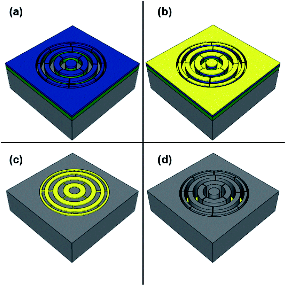 | ||
| Fig. 1 Schematic illustration of the fabrication process: (a) exposure and development of double-layer resist system (70 nm PMMA bottom – green, 40 nm ZEP7000 top – blue) on Si wafer (grey), (b) metal layer evaporation (1.5 nm Ti and 25 nm Au – yellow), (c) lift-off, and (d) MACE. | ||
The exposed ZEP7000 was developed in hexylacetate at −18 °C for 30 s and the exposed PMMA resist was developed in 1:3.5 (v/v) MIBK:IPA at 10 °C for 70 s. Subsequently, the substrates were rinsed in IPA and n-pentane, dried under a nitrogen gas flow and further descummed by oxygen plasma for 13 s for removal of any exposed PMMA/ZEP7000 residues (Fig. 1a). A 1.5 nm adhesive titanium layer was electron beam evaporated at a rate of 1 Å s−1, followed by 25 nm Au film evaporation at 2 Å s−1 with an in-house Eurovac/Thermionics deposition system (Fig. 1b). The resist lift-off was performed under gentle sonication in acetone and mr-Rem 400 at 50 °C for 5 min each (Fig. 1c). The samples were then rinsed in deionized (DI) H2O, IPA, n-pentane and dried with nitrogen gas. The resulting metal patterned Si substrates were cleaned by oxygen/argon plasma for 3 min just before the MACE processing. This plasma step was found to be necessary for removal of any surface contaminations that might prohibit the MACE process.
2.3 MACE processing of zone plates
All MACE experiments were performed in a polytetrafluorethylene bath under light protection and repeated at least three times to ensure reproducibility (Fig. 1d). The conditions for all the experiments are detailed in Table 1, where the final concentrations of the species in the etching bath are specified. The influence of oxidizing agent on zone plate MACE processing was investigated by performing H2O2 concentration series experiments using 0.17 M, 0.34 M, 0.68 M and 1.4 M H2O2 and constant HF and DI H2O concentrations of 4.7 M and 52 M, respectively. The etching solution volume was 15 ml for every MACE experiment to ensure the presence of excess reactants and was prepared by mixing the chemicals in the polytetrafluorethylene bath just before etching.| Etching condition | Concentration [HF]:[H2O2] (M) |
Temperature (°C) | Time (min) | Potential (V) |
|---|---|---|---|---|
| C1 | 4.7:0.17 |
25 | 4 | 2.66 |
| C2 | 4.7:0.34 |
25 | 4 | 2.67 |
| C3a | 4.7:0.68 |
25 | 4 | 2.68 |
| C3b | 4.7:0.68 |
25 | 8 | 2.68 |
| C3c | 4.7:0.68 |
25 | 16 | 2.68 |
| C3d | 4.7:0.68 |
25 | 32 | 2.68 |
| C4 | 4.7:1.4 |
25 | 4 | 2.69 |
| C5 | 4.7:0.68 |
10 | 4 | 2.68 |
| C6 | 4.7:0.68 |
40 | 4 | 2.68 |
The MACE experiments were performed at room temperature typically for 4 minutes. The pH of the etching solution was measured before starting and after completion of MACE experiments. The processed samples were rinsed with DI H2O and dried under nitrogen gas flow.
The influence of temperature on the MACE process was investigated by etching at 10 °C, 25 °C and 40 °C using a Lauda Eco RE620 Silver thermostat and bath for temperature control. A typical experiment was performed using a 15 ml etching solution consisting of 0.68 M H2O2, 4.7 M HF and 52 M DI H2O. Both the Au patterned Si samples and chemicals were placed in the water bath prior to the experiments for temperature equilibration. The etching solutions for each experiment were prepared right before starting the MACE process. The etching time was set to 4 min for all experiments. After completing the MACE process the samples were rinsed with DI H2O and dried under a nitrogen gas flow.
The etching depth of our zone plate design was investigated by MACE time series experiments. All experiments were performed using etching solution formulations of 0.68 M H2O2, 4.7 M HF and 52 M DI H2O. Each sample was etched in 15 ml etching solution for 4, 8, 16 and 32 min. After completing the MACE process, the samples were rinsed with DI H2O and dried with nitrogen gas.
2.4 Characterization
Electron microscope micrographs were recorded and cross-sections were obtained with a FEI NOVA 200 dual beam scanning electron microscope (SEM) and focused ion beam (FIB) system. The surface roughness was analyzed with a Bruker FastScan atomic force microscopy (AFM) system in tapping mode on Si pillar tops on the third zone of the zone plates.3 Results and discussion
The MACE process is described in detail in several reviews.6,7,11 Chemical etching of Si in HF solutions containing an oxidizing agent is known to be a mixed chemical and electroless process, i.e. a galvanic process.12,13 Briefly, an etching solution consisting of a strong oxidizing agent, H2O2 in this work, and HF is used to transfer the Au pattern into the Si substrate through a local electrochemical process. The Au layer (cathode site) catalyzes the reduction of H2O2 resulting in hole (h+) formation that subsequently is injected into the Si in contact with the cathode site. The cathode reaction can be expressed as:| H2O2(aq) + 2H(aq)+ → 2H2O(l) + 2h+ E0cat = +1.78 V | (1) |
The injected holes oxidize the Si (anode site) to silica (SiO2):
| Si(s) + 2H2O(l) + 4h+ → SiO2(s) + 4H(aq)+ E0an = +0.91 V | (2) |
In this electrochemical process there are anode and cathode sites on the surface with local currents flowing between them, as described by Turner et al.14 The local currents originate from the holes injected into Si by the oxidizing agent H2O2. By combining eqn (1) and (2), the balanced redox reaction can be expressed as:
| Si(s) + 2H2O2(aq) → SiO2(s) + 2H2O(l) E0cell = +2.69 V | (3) |
The formation of SiO2 is followed by the dissolution due to the presence of excessive HF in the etching solution, forming SiF62− ions according to the following reaction:
| SiO2(s) + 6HF(aq) → SiF6(aq)2− + 2H2O(l) + 2H(aq)+ | (4) |
By combining eqn (3) and (4) the overall MACE reaction mechanism using H2O2 as the oxidizing agent can be expressed as:
| Si(s) + 2H2O2(aq) + 6HF(aq) → SiF6(aq)2− + 2H(aq)+ + 4H2O(l) | (5) |
When the redox reaction in eqn (3) is considered, the resultant net positive potential is indicative of the spontaneous, i.e. galvanic, process. The effect of different parameters, as the concentration of chemical species and the temperature, on the cell potential can be calculated by the Nernst equation:
 | (6) |
485 C mol−1 is the Faraday constant, T is the absolute temperature in Kelvin and n is the number of moles of electrons/holes transferred in the balanced redox reaction. K represents the equilibrium constant for the balanced redox reaction, and considering eqn (3) it leads to K = 1/[H2O2]2, where [H2O2] is the equilibrium concentration of H2O2. The Nernst equation for the overall redox process then can be expressed as:
 | (7) |
According to eqn (7), the expected cell potential is calculated for a series of investigated H2O2 concentrations, and processing temperatures (Table 1). With increasing concentration of H2O2 from 0.17 M to 1.4 M (C1–C4) the cell potential shows a slightly increasing trend. This is an indication of an increase in the formation and injection rate of holes into Si. Although the temperature does not have a big influence on the calculated cell potential (C3, C5 and C6), it may influence the kinetics of the hole injection into Si. However, the temperature is expected to significantly influence the dissolution rate of SiO2 by HF (eqn (4)). The H2O2 concentration, thus, can be considered as the equivalent of the current density in electrochemistry, and therefore the redox reaction rate, while the HF concentration controls the surface chemistry and the dissolution of SiO2.12
3.1 Investigation of etching solution
The oxidizing agent (H2O2) is the etching rate determining reactant at relatively high HF concentrations due to the fast dissolution rate of oxidized Si at the Au–Si interface.12 Therefore, four different H2O2 concentrations were investigated at room temperature while keeping the HF content constant (4.7 M) (Table 1, C1–C4) for 4 min etching time. We have based our selection of the concentration of HF on the reported value used in the literature for MACE processing of Si-based zone plates.9,10 In general, all etching solutions resulted in successful, vertical etching across the whole zone plate (Fig. 2a–d).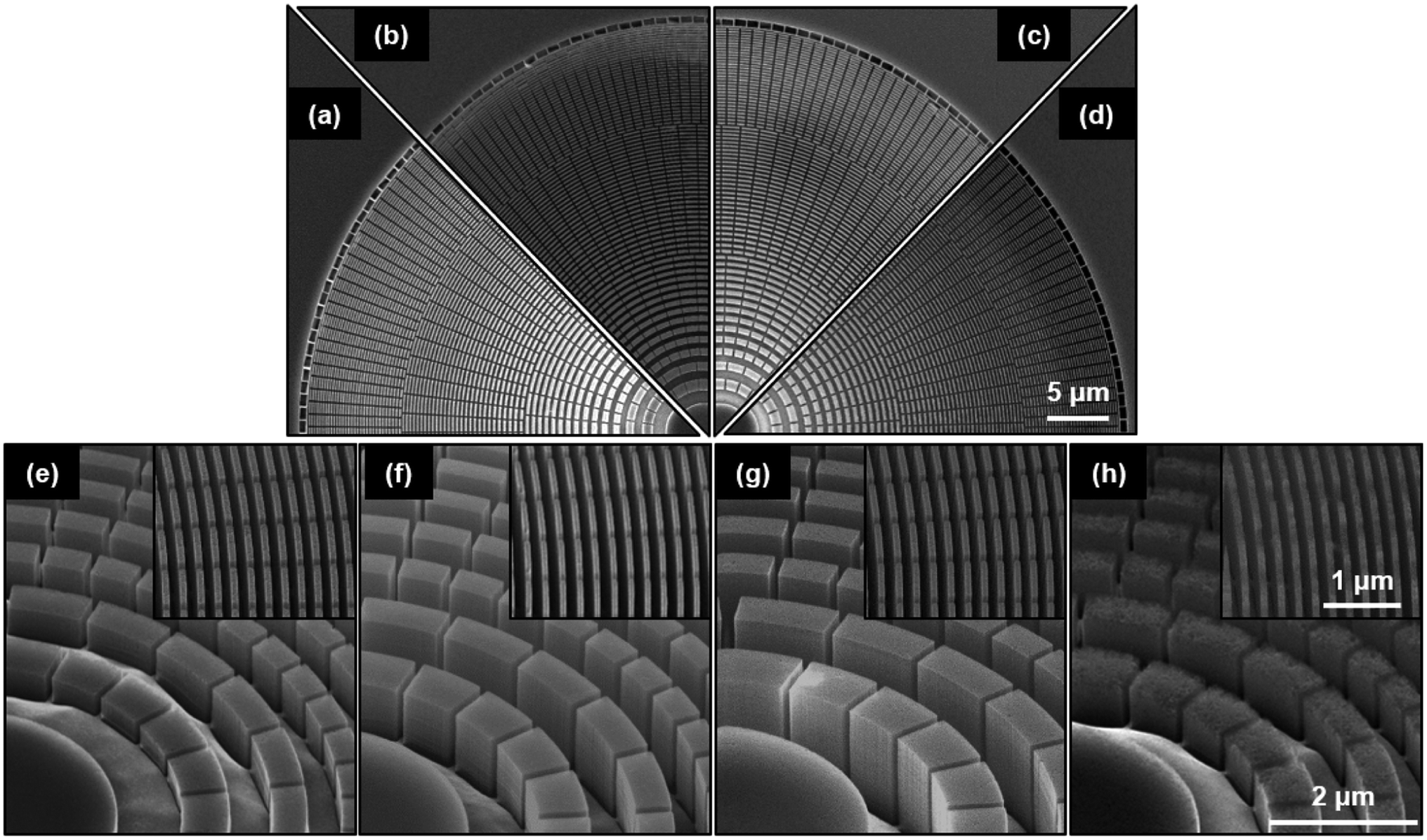 | ||
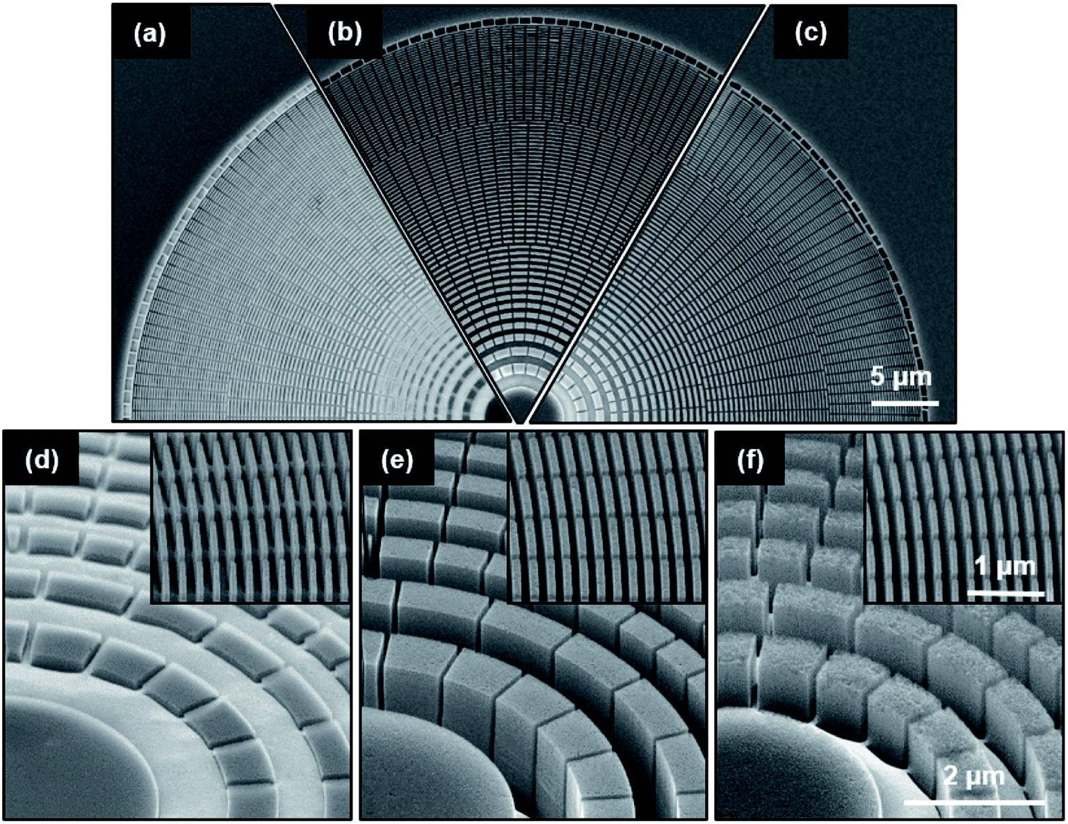
| Fig. 2 SEM micrographs of zone plates etched at different HF:H2O2 concentrations at 25 °C, where HF:H2O2 concentrations are: (a and e) 4.7 M:0.17 M (C1); (b and f) 4.7 M:0.34 M (C2); (c and g) 4.7 M:0.68 M (C3a) and (d and h) 4.7 M:1.4 M (C4). Same scale bar applies to (a)–(d) and (e)–(h). The insets in (e)–(h) show the outermost zones. | ||
The etching solution with lowest H2O2 concentration of 0.17 M (C1) resulted in the smallest (≈0.70 μm) etching depth (Fig. 2e). By doubling the H2O2 concentration to 0.34 M (C2) the etching depth increased (≈1.3 μm) (Fig. 2f). The deepest etching (≈2.6 μm) was observed for zone plates processed with 0.68 M H2O2 (C3a) (Fig. 2g). This trend is expected since elevation of H2O2 concentration in the etching solution should increase the local current density, which in turn increases the etching rate and depth due to the presence of excess HF in the system. A similar trend has been reported for very close concentrations of HF:H2O2, by Chartier et al., for etching Si with isolated Ag nanoparticles.12
Interestingly, the etching solution with the highest H2O2 concentration of 1.4 M (C4) deviated from the previously mentioned trend, yielding a shallower etched Si. The etching depth is only ≈0.87 μm (Fig. 2h). Furthermore, significant roughness was observed on top of the zones indicating porous Si formation and/or electro-polishing. We propose the following explanation for this behavior. The high H2O2 concentration yields a higher hole density in the etching solution and thus a higher hole injection rate at the Au–Si interface. If this rate is higher than the Si dissolution rate, holes can diffuse in an uncontrolled manner, and to longer diffusion distance, from the Au–Si interface into the material, resulting in oxidation and subsequently dissolution of Si at unwanted sites. This indicates that more holes are consumed at zone sidewalls than at the zone base. Although the etching depth is expected to increase due to the higher concentration of H2O2, the etching process did not go linearly into the substrate but was rather random around the walls. Therefore, increased wall roughness could be attributed to a more diffuse and faster hole injection rate due to enhanced local electric field at the Au–Si contact region. This may be a result of our zone plate pattern design where the cathode (Au) surrounds the anode (Si) thus allowing local enhancement of electric field (cp. Sect. 3.4). We therefore expect that the surface roughness observed in the SEM images on top of the zones to be also present on the sidewalls of the zones. A similar trend of increased roughness (or porosity) has been reported by Chartier et al. for etching Si with isolated Ag nanoparticles,12 when increasing the H2O2 concentration while keeping the concentration of HF constant.
Since zone side-wall roughening affects the diffraction efficiency of the zone plates in a negative way,15 we investigated the roughness for the samples with unexpected etching behavior using AFM. For the highest H2O2 concentration (C4) the surface roughness was 2.3 nm rms. In contrast, solution C3a showed only a roughness of 0.56 nm rms. Since the etching solution C3a also showed the most profound etching depth, it was selected for further investigations on the reaction parameters of temperature and time.
3.2 Investigation of etching temperature
Previous work on the fabrication of zone plates with MACE process used temperatures between 6–10 °C without further elaboration of this choice.9,10 In general, hole production via reduction of H2O2 and hole injection rate into Si should be a function of temperature, and accordingly Cheng et al.16 and Backes et al.17 report an increase in etching depth at higher temperatures. In order to better understand our process and eventual benefits of non-room-temperature processing, we investigated the MACE process at two additional temperatures of 10 °C (C5) and 40 °C (C6) and compared results for 4 min etching time with the ones obtained previously at 25 °C (C3a) with the HF:H2O2 concentrations of 4.7 M:0.68 M (Table 1).
All investigated MACE processing temperatures resulted in vertical etching across the whole zone plate (Fig. 3a–c). The zone plates etched at 10 °C (C5) had the smallest depth (≈0.32 μm), as expected, due to slower hole injection and dissolution rates at lower temperature (Fig. 3d). As described in the previous section, greater etching depth (≈2.6 μm) was obtained for the zone plates etched at 25 °C (C3a, Fig. 3e). The zone plates processed at 40 °C (C6, Fig. 3f) had a smaller etching depth (≈1.2 μm) compared to the zone plates processed at 25 °C, which is against the expected trend. Furthermore, the zones showed a surface roughness of 3.8 nm rms in the AFM measurements probably as the result of an imbalance in the hole injection and the dissolution rates. We note that zone plates processed at 40 °C look very similar to zone plates obtained using high H2O2 concentration (HF:H2O2 concentrations of 4.7 M:1.4 M) (Fig. 2h). This might indicate the processing in a similar MACE regime.
 | ||
| Fig. 3 SEM micrographs of zone plates etched with HF:H2O2 concentrations of 4.7 M:0.68 M for 4 min at different temperatures: (a and d) 10 °C (C5); (b and e) 25 °C (C3a) and (c and f) 40 °C (C6). Same scale bar applies to (a)–(c) and (d)–(f). The insets in (d)–(f) show the outermost zones. | ||
The results from the investigation of etching solution composition and temperature indicate that a balanced MACE reaction with adjusted hole injection and SiO2 dissolution rate is crucial in order to obtain vertical and smooth nanostructures. We find this regime at room temperature, which offers important advantages compared to other conditions; specifically, no need for temperature modulation (heating or cooling) and relatively fast etching rate (≈0.7 μm min−1).
3.3 Etching time
The efficiency of zone plates shows a maximum at a certain depth of the nanostructures for a given X-ray energy. Therefore, a constant MACE speed would be important since the final zone depth could simply be adjusted by the etching time. Consequently, we investigated the depth of Si nanostructures using our selected solution with HF:H2O2 concentrations of 4.7 M:0.68 M at 25 °C for four different processing times ranging from 4 min to 32 min (Table 1, C3a–C3d).
Fig. 4 shows the results of the etching depth as a function of etching time in a graphical form. The etching depth increases linearly with etching time and has a rate of ≈0.7 μm min−1. The differences in zone thickness within the zone plate, indicated by the error bars in Fig. 4, are a result of the characteristic zone plate pattern. The width of the zones decreases towards the outer parts of the zone plate from 1 μm to 100 nm and consequently etching depth varies slightly (4–6% for all samples). Nevertheless, this very low variation highlights the fact that the dissolution of Si is homogeneous even in the narrowest part of the zone plate. The diffusion of etching solution and byproducts in and out from the nanostructures seems to be free even at large aspect ratios (narrow channels). Furthermore, no measurable change in pH of the etching solution was detected before and after MACE processing for 32 min (pH = 0–0.5). This is probably due to a negligible change in the HF concentration because of the small size of processed zone plates with respect to the bath volume. It should be possible to continue the MACE process for longer time periods than 32 min and larger etching depth without the need of replenishing the etching bath.
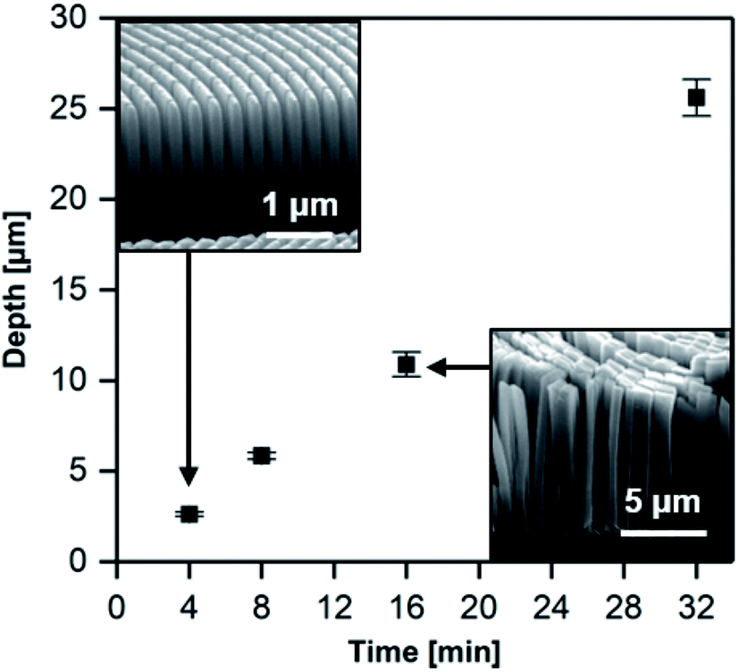 | ||
| Fig. 4 Zone plate etch depth as a function of etching time, based on image analysis of SEM cross-section micrographs. The error bars represent the variation in etching depth measurements along the etching profile for a given condition. The insets are SEM micrographs of typical cross-sections of zone plates etched for 4 min (C3a) and 16 min (C3c). | ||
3.4 Pattern design
An interconnected, grid-like Au catalyst pattern was used in the MACE processing of Si zone plates. Although the pattern design is not a parameter in the present study, it does have an influence on MACE process results. Therefore we want to detail here some of our findings.It seems to be beneficial to have a design where the Au catalyst zone plate rings are interconnected. Our attempts to etch normal zone plate (made of concentric Au rings) patterns did not yield a reproducible, good quality pattern transfer into the Si. The rings of the zones did not etch down vertically into the Si in a controlled way. In contrast, by adding small Au interconnects the etching became vertical and homogeneous over the whole zone plate (Fig. 2 and 3). We attribute this to a situation where charges can distribute evenly in the Au catalyst-Si interface. Additionally, the interconnects prohibit non-vertical motion of the catalyst during MACE process, something often observed for isolated catalytic nanoparticles.6 Interconnectivity helps etchants and formed products to move in and out allowing quick replenishment of the reagents at the catalytic sites.
A disadvantage of a totally interconnected design is that it will result in free-standing Si nanopillars. For very high aspect ratios and smallest zone sizes, these pillars will become mechanically unstable. Our pattern design resulted in free-standing and stable Si structures for up to 8 min etching time at ≈6 μm depth. At longer processing time the Si pillars collapsed (see inset in Fig. 4). It is important to note that we did not dry our samples in a critical point dryer, which could prevent the collapse of deeper structures.
A possible alternative to improve the stability of the Si nanostructures is the addition of Si interconnects or anchors. This was already demonstrated by Chang et al.9 and Li et al.10 We also investigated such designs but with limited success. We observed that the loose ends of Au catalyst, especially in the outer part of the zone plate, at random positions started to etch in a non-vertical direction (Fig. 5). One could shorten the length of these Au parts as done in Li et al.10 to minimize this effect, however, this will increase the number of interconnects and further reduce the active zone plate area and consequently the efficiency.
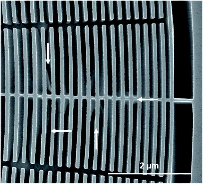 | ||
| Fig. 5 Zone plate design with Si interconnects etched with HF:H2O2 concentrations of 4.7 M:0.68 M for 4 min at 25 °C (C3a). Arrows indicate positions with non-vertical etching behavior of Au catalyst stripes. This specific zone plate was on the same Si wafer as the zone plate presented in Fig. 2(c and g) and processed under exactly identical conditions. | ||
Finally, Chang et al.9 first proposed the utilization of a large Au ring around the zone plate as a electron hole balancing structure necessary for vertical MACE. Accordingly, we also added a ring consisting of small Au rectangles to our pattern design (Fig. 5). Although our ring is only 500 nm wide and considerably smaller than the one used in Chang et al.,9 we still obtain vertical etching for all conditions investigated in our study. This, together with the above mentioned observations, makes us believe that an interconnected grid design is the key for our highly hierarchical vertical zone plate MACE processing in a highly reliable, reproducible and scalable level.
4 Conclusion
We demonstrated the significance of etching solution composition and temperature for controlling MACE processing of Si-based zone plates. Our results revealed that the process can be controlled at room temperature in an etching bath, yielding a high etching rate of ≈0.7 μm min−1, resulting in vertical, high aspect ratio Si nanostructures. This is about an order of magnitude faster than previously reported results.9,10 At some tested temperatures and etching bath compositions the etching process did not translate linearly into the Si substrate but rather diffused into the Si walls, producing rough Si surfaces. This is an important finding that is linked to our specific zone plate pattern design with interconnected Au rings, enhancing local electric fields at the Au–Si contact region. The room-temperature MACE process developed in this work is well suited for the fabrication of X-ray zone plates, since high aspect ratio structures can be conveniently obtained within only a few minutes etching time. We believe our findings provide insight for Si processing, microfabrication and nanomaterials fabrication fields. The developed fabrication procedure with a grid catalyst design and an optimized etching solution can be used for nanostructuring Si for a wide-range of applications.Conflicts of interest
There are no conflicts to declare.Acknowledgements
This work was supported by the Swedish Research Council. We thank Adem B. Ergul for help with the cross-section images and Jussi Rahomäki for starting with MACE in our group.References
- F. Priolo, T. Gregorkiewicz, M. Galli and T. F. Krauss, Nat. Nanotechnol., 2014, 9, 19–32 CrossRef CAS PubMed.
- D. Fine, A. Grattoni, R. Goodall, S. S. Bansal, C. Chiappini, S. Hosali, A. L. van de Ven, S. Srinivasan, X. Liu, B. Godin, L. Brousseau, I. K. Yazdi, J. Fernandez-Moure, E. Tasciotti, H. J. Wu, Y. Hu, S. Klemm and M. Ferrari, Adv. Healthcare Mater., 2013, 2, 632–666 CrossRef CAS PubMed.
- G. Schierning, Phys. Status Solidi A, 2014, 211, 1235–1249 CrossRef CAS.
- S. A. Kara, A. Keffous, A. M. Giovannozzi, A. M. Rossi, E. Cara, L. D'Ortenzi, K. Sparnacci, L. Boarino, N. Gabouze and S. Soukane, RSC Adv., 2016, 6, 93649–93659 RSC.
- B. Wu, A. Kumar and S. Pamarthy, J. Appl. Phys., 2010, 108, 051101 CrossRef.
- Z. Huang, N. Geyer, P. Werner, J. De Boor and U. Gösele, Adv. Mater., 2011, 23, 285–308 CrossRef CAS PubMed.
- X. Li, Curr. Opin. Solid State Mater. Sci., 2012, 16, 71–81 CrossRef CAS.
- I. Mohacsi, I. Vartiainen, B. Rösner, M. Guizar-Sicairos, V. A. Guzenko, I. McNulty, R. Winarski, M. V. Holt and C. David, Sci. Rep., 2017, 7, 43624 CrossRef.
- C. Chang and A. Sakdinawat, Nat. Commun., 2014, 5, 1–7 Search PubMed.
- K. Li, M. J. Wojcik, R. Divan, L. E. Ocola, B. Shi, D. Rosenmann and C. Jacobsen, J. Vac. Sci. Technol., B: Nanotechnol. Microelectron.: Mater., Process., Meas., Phenom., 2017, 35, 06G901 Search PubMed.
- H. Han, Z. Huang and W. Lee, Nano Today, 2014, 9, 271–304 CrossRef CAS.
- C. Chartier, S. Bastide and C. Lévy-Clément, Electrochim. Acta, 2008, 53, 5509–5516 CrossRef CAS.
- E. S. Kooij, K. Butter and J. J. Kelly, Electrochem. Solid-State Lett., 1999, 2, 178–180 CrossRef CAS.
- D. R. Turner, J. Electrochem. Soc., 1960, 107, 810 CrossRef CAS.
- G. Schneider, Appl. Phys. Lett., 1998, 73, 599–601 CrossRef CAS.
- S. L. Cheng, C. H. Chung and H. C. Lee, J. Electrochem. Soc., 2008, 155, D711 CrossRef CAS.
- A. Backes, M. Leitgeb, A. Bittner and U. Schmid, ECS J. Solid State Sci. Technol., 2016, 5, P653–P656 CrossRef CAS.
| This journal is © The Royal Society of Chemistry 2018 |