
 Open Access Article
 This Open Access Article is licensed under a
 Creative Commons Attribution 3.0 Unported Licence
Totally room-temperature solution-processing method for fabricating flexible perovskite solar cells using an Nb2O5–TiO2 electron transport layer†
Jun Jiang,
Shubo Wang,
Xuguang Jia ,
Xiang Fang,
Shuai Zhang,
Jing Zhang,
Wei Liu,
Jianning Ding* and
Ningyi Yuan*
,
Xiang Fang,
Shuai Zhang,
Jing Zhang,
Wei Liu,
Jianning Ding* and
Ningyi Yuan*
School of Materials Science and Engineering, Jiangsu Collaborative Innovation Center of Photovoltaic Science and Engineering, Jiangsu Province Cultivation Base for State Key Laboratory of Photovoltaic Science and Technology, Changzhou University, Changzhou 213164, Jiangsu, China. E-mail: dingjn@cczu.edu.cn; nyyuan@cczu.edu.cn
First published on 3rd April 2018
Abstract
Flexible perovskite solar cells are new technology-based products developed by the global solar industry and are promising candidates for realizing a flexible and lightweight energy supply system for wearable and portable electronic devices. A critical issue for flexible perovskite solar cells is to achieve high power conversion efficiency (PCE) while using low-temperature solution-based technology for the fabrication of a compact charge collection layer. Herein, we innovatively introduce niobium ethoxide as a precursor additive to TiO2 NCs, which allows realization of an Nb2O5–TiO2 electron transport layer (ETL). The presence of Nb2O5 remarkably enhances electron mobility and electrical conductivity of the ETLs. In addition, uniform perovskite films are prepared by an annealing-free solution-based method. The excellent performance of the cell is attributed to its smooth film surface and high electron mobility, and performance is verified by the effective suppressions of charge recombination and time-resolved photoluminescence. PCEs of 15.25% and 13.60% were obtained for rigid substrates (glass/fluorine-doped tin oxide) and an indium tin oxide/PET (poly(ethylene terephthalate)) flexible substrate by using a totally room-temperature solution-processing method, respectively.
1. Introduction
Perovskite solar cells have developed very rapidly over the last several years and could be in considerable demand for various applications in the future photovoltaic market.1–6 Numerous scientific research professionals have accelerated increases in power conversion efficiency (PCE) of perovskite solar cells, and at present, the certified world record for a PCE is 22.1%.7 As a light absorption layer, APbX3 (A = CH3NH3, (NH2)2CH2 or Cs, and X = I, Br, or Cl) is considered as the most promising replacement for silicon solar cells; APbX3 has outstanding properties such as strong light absorption, weakly bound excitons, long-range charge-carrier diffusion, and apparent tolerance to defects.8–10A state-of-the-art photovoltaic solar cell (PSC) is prepared in a conventional n-i-p device configuration consisting of an n-type oxide semiconductor capped with a perovskite absorber and a hole-transport layer (HTL). The electron transfer layer (ETL) of PSCs plays important roles in extracting electrons and blocking holes from perovskite. Metal oxide materials such as TiO2, ZnO, and SnO2 are widely used in most studies aimed at achieving high efficiency because of their environmentally friendly nature, wide band gap, high electron mobility, and good stability.11–14 A large number of PSCs based on TiO2 require a high-temperature sintering process for their crystallization or removal of the dispersion medium.8–10,15 However, TiO2, ZnO, and SnO2 ETLs obtained using high-temperature treatment cannot be applied to flexible perovskite solar cells. Recently, methods have been developed for fabricating low-temperature processable TiO2 ETLs for planar PSCs, such as atomic layer deposition16 and magnetron sputtering.17 Compared to vacuum methods, solution-based techniques are generally more cost-effective and scalable and can be used to achieve roll-to-roll process-ability. Therefore, it is imperative to develop effective methods that can restriction migration, improve electron mobility of an ETL, and reduce trap-state density within the perovskite material, thereby eliminating hysteresis and improving the efficiency of PSCs. However, perovskite materials such as CH3NH3PbI3 and CH(NH2)2PbI3 are mostly used for PSCs, and these materials practically need annealing for 10–60 min to form the black crystalline photoactive layer.18–23 Annealing process is not convenient for mass production because it requires additional equipment and increases energy consumption. One method to address this problem is to employ annealing-free processing,15 which can save energy and facilitate industrial production. Herein, we propose a facile strategy to prepare a highly efficient perovskite solar cell via room-temperature solution processing. TiO2 films are fabricated by spin coating a colloidal solution of anatase TiO2 nanocrystallines (NCs) prepared via a low-temperature sol–gel method on a substrate. Considering improved performance of the film, we employed niobium ethoxide as a precursor additive. Nb2O5 is considered a better ETL for a perovskite solar cell due to its higher carrier mobility and conduction band edge position. Here, niobium ethoxide is introduced into the TiO2 dispersion as an aid dispersant. Niobium ethoxide facilitates spontaneous coalescence of the TiO2 NCs, thereby forming a stable dispersion. The stable dispersion is spin-coated onto the conductive base film without annealing; only ultraviolet (UV) treatment for 15 min yields a uniform and dense Nb2O5–TiO2 layer. It is expected that the Nb2O5 formed in situ would passivate the grain boundary of the TiO2 NCs, and further form a dense and uniform film. The exceptional performance of the layer is attributed to the excellent optical and electronic properties of the Nb2O5–TiO2 material, such as a smooth surface and high electron mobility; these properties make the material a better growth platform for a high-quality perovskite absorber layer. In addition, MAPbI3 films are deposited as a light absorption layer via one-step spin-coating by a simple annealing-free process.
2. Experimental section
2.1. Materials
4-tert-Butylpyridine (t-BP), Li-bis-(trifluoromethanesulfonyl)imide (Li-TFSI), PbI2 (99.9985%), niobium ethoxide (99.999%), dimethylacetamide (DMAc) and N-methyl-2-pyrrolidone (NMP) were ordered from Alfa Aesar; the methylammonium iodide (MAI) (99.5%), and 2,2′,7,7′-tetrakis[N,N-di(4-methoxyphenyl)amino]-9,9′-spiro-bifluorene (spiro-OMeTAD) (99.8%) were purchased from Xi'an p-OLED Technology Corp. Titanium tetrachloride (TiCl4, anhydrous, 99.5%) and chlorobenzene (anhydrous, 99.9%) were purchased from Aldrich (USA). All solvents were used without any further purification.2.2. Synthesis of TiO2 NCs and preparation of TiO2 dispersion with niobium ethoxide
TiO2 NCs were synthesized by a non-hydrolytic sol–gel reaction according to a modified procedure.24 The resulting precipitates were washed by adding excess ethanol and diethyl ether and purified by centrifugation at 3000 rpm for 5 min. This washing procedure was repeated thrice. To obtain the TiO2 colloidal solution (∼5 mg mL−1), the washed TiO2 NCs were dispersed into anhydrous methanol, and ultrasonic treatment was carried out for several hours. To obtain a niobium ethoxide/TiO2 mixed precursor suspension for spin coating, the purified TiO2 NCs (5 mg mL−1) were re-dispersed in ethanol at the desired niobium ethoxide concentration. Nb2O5–TiO2 ETLs were fabricated by spin-coating at 3000 rpm under ambient conditions, and the films were free from annealing. The samples were treated again with UV–ozone for 15 min before perovskite deposition.2.3. Device fabrication
Pre-patterned transparent conducting oxide substrates were sequentially cleaned using ethanol, acetone, isopropanol, and ethanol separately in an ultrasonic bath for 20 min each and then dried under flowing nitrogen. Fluorine-doped tin oxide (FTO) substrates underwent UV–ozone treatment (Model UV-03 UVO3 cleaner) for 15 min before they were used for spin-coating ETLs.A highly dispersed solution of TiO2 NCs and TiO2 NCs with niobium ethoxide in ethanol were dropped onto substrates and immediately spin-coated at a speed of 3000 rpm for 30 s. The samples again underwent UV–ozone treatment for 15 min before perovskite deposition. Then, the TiO2 (Nb2O5–TiO2)-coated substrates were transferred immediately to a nitrogen-filled glovebox for the deposition of perovskite films.
A MAPbI3 solution was prepared according to an annealing-free process reported by Fang et al.15 The MAPbI3 precursor solution (1.2 M) was prepared using a mixed solvent of DMAc and NMP in a volume ratio of 5![[thin space (1/6-em)]](https://www.rsc.org/images/entities/char_2009.gif) :1. Perovskite films were deposited onto the TiO2 or Nb2O5–TiO2 substrates according to a two-step spin-coating procedure. In the first step, spin coating was carried out at 1000 rpm for 20 s with an acceleration of 200 rpm s−1. In the second step, spin coating was carried out at 5000 rpm for 45 s with an acceleration of 1000 rpm s−1. During the second step, chlorobenzene was dropped onto the spinning substrate at 35 s before the end of the procedure. At the end of the second step, a dark perovskite film was directly formed. A spiro-OMeTAD HTL was prepared according to a process reported by Yang et al.25 The HTL was fabricated as follows: a spiro-OMeTAD solution (90 mg mL−1) was dissolved in chlorobenzene using 36 μL 4-tert-butylpyridine and 22 μL lithium bis(trifluoromethylsulfonyl)imide (520 mg mL−1) as the dopants in acetonitrile. The spiro-OMeTAD solution was spin-coated onto the perovskite films at 3000 rpm for 30 s. Finally, an 80 nm thick gold coating was deposited using a thermal evaporator.
:1. Perovskite films were deposited onto the TiO2 or Nb2O5–TiO2 substrates according to a two-step spin-coating procedure. In the first step, spin coating was carried out at 1000 rpm for 20 s with an acceleration of 200 rpm s−1. In the second step, spin coating was carried out at 5000 rpm for 45 s with an acceleration of 1000 rpm s−1. During the second step, chlorobenzene was dropped onto the spinning substrate at 35 s before the end of the procedure. At the end of the second step, a dark perovskite film was directly formed. A spiro-OMeTAD HTL was prepared according to a process reported by Yang et al.25 The HTL was fabricated as follows: a spiro-OMeTAD solution (90 mg mL−1) was dissolved in chlorobenzene using 36 μL 4-tert-butylpyridine and 22 μL lithium bis(trifluoromethylsulfonyl)imide (520 mg mL−1) as the dopants in acetonitrile. The spiro-OMeTAD solution was spin-coated onto the perovskite films at 3000 rpm for 30 s. Finally, an 80 nm thick gold coating was deposited using a thermal evaporator.
2.4. Characterization
Morphologies of the TiO2 films were characterized by field-emission scanning electron microscopy (FESEM, Zeiss Supra 55). The ζ-potential of the TiO2 NCs with different concentrations of niobium ethoxide was characterized by using a size analyzer (Zetasizer Nano ZS ZEN3600 instrument, Malvern Instruments) at room temperature with a 633 nm laser. The UV-vis transilluminator spectra of the samples were recorded on a spectrophotometer (UV5800). High-resolution transmission electron microscopy (HR-TEM) was carried out using an electron microscope (JEM-2100, JEOL Ltd., Japan). The root-mean-square (RMS) roughness and topography images of the films were obtained via atomic force microscopy (AFM, Veeco Dimension V). The quality and crystalline structure of the samples were confirmed by θ–2θ X-ray diffraction (XRD) using an X-ray diffractometer (D/max 2500 PC) with a Cu Kα radiation source. A photoluminescence (PL) system (DeltaFlex, Horiba Ltd.) was used to measure the time-resolved PL (TRPL) decay. Photovoltaic performance of the solar cells was measured using a multisource meter (Model 2400, Keithley, Cleveland, OH, USA) under one sun (AM 1.5G, 100 mW cm−2) illumination, which was achieved by using a solar simulator (500 W Xe lamp) (XES-40S1, San-Ei Electric Co., Ltd., Japan) as the light source. The device area of 0.07 cm2 was defined by a metal mask. All devices were scanned with a reverse and forward under standard test procedure at a scan rate of 0.2 V s−1. X-Ray photoelectron spectroscopy (XPS) was performed on a photoelectron spectrometer (ESCALAB 250Xi, Thermo Fisher Scientific).3. Results and discussion
3.1. Characterization of TiO2 and Nb2O5–TiO2 films
In the spin-coating process, a stably distributed precursor solution of TiO2 NCs in solution is a prerequisite to form uniform and void-free TiO2 thin films. The niobium ethoxide-capped TiO2 NCs have a uniform dispersion in ethanol, are stable for months, and have better anti-settleability properties (Fig. S1†). The ζ-potential is an important factor reflecting colloid stability. The ζ-potential was measured, and the results are shown in Fig. 1. The figure indicates that the ζ-potential value for TiO2 is 16.3 mV. The ζ-potential increases with the addition of niobium ethoxide. It demonstrated that the niobium ethoxide plays an important role in the dispersion of TiO2 NCs. Powder XRD measurements of a TiO2 sample revealed typical diffraction peaks of anatase TiO2 (Fig. 2a). The diffraction peaks centered at 25.063, 37.682, 47.882, 54.119, 62.418, and 75.029 are assigned to (101), (004), (200), (105), (204), (116), and (215) diffractions, respectively. This result confirms that the as-synthesized TiO2 NCs are assigned to the anatase crystal structure (PDF no. 21-1272). Scherrer peak width analysis26 revealed that the average size of the nanocrystalline domains is approximately 8.8 nm. To gain further insights into the nanoscale morphology and nanocrystal structures, the morphology of as-synthesized TiO2 NCs was investigated using the HR-TEM images. The HR-TEM images (Fig. S2a†) revealed that the TiO2 NCs are around 5–10 nm in diameter, which is consistent with the value obtained by Scherrer peak width analysis. In addition, the selected area electron diffraction pattern for the TiO2 NCs (Fig. S2b†) confirms the high crystallinity of the TiO2 NCs.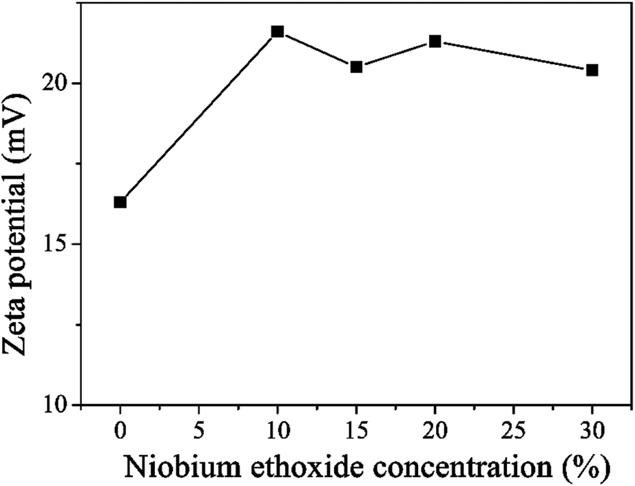 | ||
| Fig. 1 The zeta potential of TiO2 NCs with different concentration of niobium ethoxide. | ||
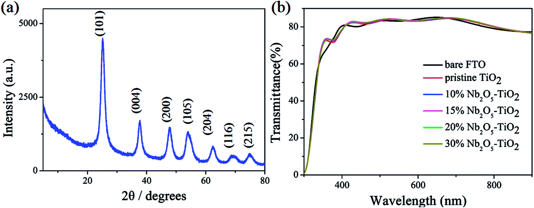 | ||
| Fig. 2 (a) Powder X-ray diffraction pattern of TiO2 NCs. (b) Transmittance spectra of bare FTO, pristine TiO2, and Nb2O5–TiO2 with different niobium ethoxide contents. | ||
Fig. 2b shows the optical transmission spectra of TiO2 and Nb2O5–TiO2. Both the materials show excellent transmittance in the wavelength range of 400–800 nm. The resultant ETLs coated on the FTO glass substrates shows good optical transparency and higher transmittance than the bare FTO glass, with the transmittance being greater than 80% in the entire visible region. The high transparency of the Nb2O5–TiO2 ETLs is very conducive to the light absorption of the perovskite layer and improves light harvesting. No apparent difference was found between the transmittances of different Nb2O5–TiO2 films deposited on the FTO substrates.
The composition and bonding type of the Nb2O5–TiO2 film were measured using XPS. A typical XPS spectra of Nb2O5–TiO2 is shown in Fig. 3a. Clearly, the O, Ti, and Nb peaks are located at ∼530.59, ∼458.99, and ∼207.51 eV, respectively. The high-resolution Ti 2p (Fig. 3b) spectrum reveals two different peaks located at 459.04 and 464.69 eV, which correspond to Ti 2p3/2 and Ti 2p1/2, respectively; accordingly, a spin–orbit coupling of 5.65 eV is obtained, which is the signature of Ti4+. As shown in the Nb 3d core level spectra (Fig. 3c), Nb 3d5/2 and Nb 3d3/2 peaks are located at 207.54 and 210.20 eV, respectively, indicating the presence of five-valent niobium in the deposited films.27 The main binding energy of 530.3 eV is attributed to O 1s (Fig. 3d) which indicates the O2− state in TiO2 and the peak at the higher binding energy of 531.4 eV is attributed to surface oxygen-group absorbance or hydroxyl groups.28–31
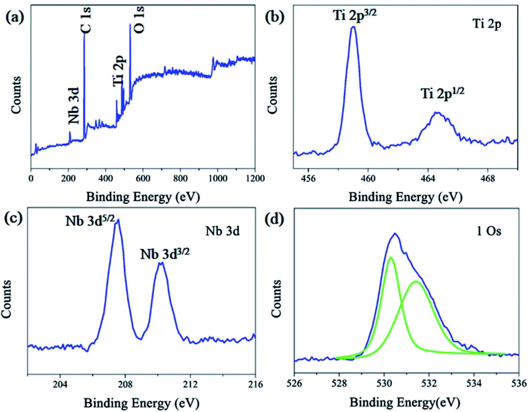 | ||
| Fig. 3 (a) Typical XPS survey of Nb2O5–TiO2 film. High-resolution XPS (b) Ti 2p, (c) Nb 3d, and (d) O 1s peaks of the Nb2O5–TiO2 film deposited on a glass substrate. | ||
Fig. 4a and b show the top-view SEM images of the TiO2 and Nb2O5–TiO2 films. The Nb2O5–TiO2 film is uniform and dense and shows no apparent pinholes, indicating the high quality of the film. The surface morphology of the Nb2O5–TiO2 film is not like to that of the pristine TiO2 film. The results of simultaneous energy-dispersive spectroscopy (EDS) of the Nb2O5–TiO2 film are shown in Fig. S3.† When excess niobium ethoxide (30% and 40%) is added, the surface morphology indicates the formation of a porous surface with a large number of pinholes, directly causing a deterioration in the quality of the thin film (Fig. S4†). Fig. 4c and d shows the AFM height images of the TiO2 and Nb2O5–TiO2 films. The RMS roughness decreased from 13.8 to 10.5 nm because of the introduction of Nb2O5, indicating that the Nb2O5–TiO2 films have flat surfaces. A smooth surface is essential for growing high-quality perovskite films, reducing surface defect trap interfaces with ETLs and HTLs, and enhancing charge extraction at the interface between the ETL and the perovskite layer.32–34
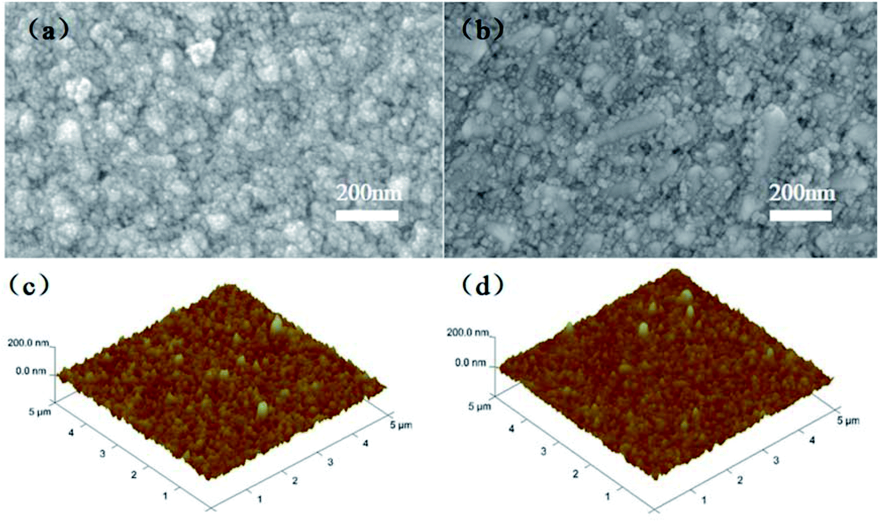 | ||
| Fig. 4 Top-view SEM images of (a) TiO2 and (b) Nb2O5–TiO2 films coated on FTO substrates. AFM height images of the (c) TiO2 and (d) Nb2O5–TiO2 films. | ||
To investigate the effect of introducing Nb2O5 on the electrical properties, the electron mobility was studied by the space charge limited current (SCLC) method using an electron-only device structure. The sample structure used for this measurement was FTO/PCBM/TiO2 (15% Nb2O5–TiO2)/PCBM/Ag. The details are shown in the ESI.† Fig. S5† shows the current density–voltage (J–V) curves for the TiO2 and Nb2O5–TiO2 films fitted using the Mott–Gurney law.34,35 It's apparent that the electron mobility of the ETL film increases considerably because of the introduction of Nb2O5. The electron mobility increases from 7.09 × 10⁻⁴ to 1.14 × 10⁻³ cm2 V−1 s−1, which is very close to previous reports that TiO2 modified craft with annealing process.36
3.2. Photovoltaic performance
The above measurements show that the quality of the TiO2 NCs film improves considerably because of the introduction of Nb2O5; e.g., the film has a smoother surface and enhanced electron mobility. Next, PSCs were designed and fabricated using the TiO2 and Nb2O5–TiO2 ETLs. Fig. S6† shows the detailed device structure, in which FTO is employed as the anode, the TiO2 or Nb2O5–TiO2 film as the ETL, MAPbI3 as the absorber layer, spiro-OMeTAD as the HTL, and a gold layer as the cathode. A cross-sectional SEM image of the completed device architecture is shown in Fig. S7.† The smooth morphology of the Nb2O5–TiO2 films is beneficial for forming highly crystalline and compact perovskite films. Fig. S8† shows the top-view SEM images of the perovskite film, which exhibits smooth surfaces, big crystalline size, and good coverage. Table S1† lists the device performance optimized as a function of the Nb2O5 content; the key J–V parameters are summarized in ESI.† It appears that the PCE increased from 13.47% to 15.25%. It is apparent that at the optimum Nb2O5 content, the device performance reaches over 15%. The corresponding photovoltaic parameters for the champion cells are summarized in Table 1. The PSCs based on TiO2 ETLs have a short-circuit current density (Jsc) of 19.55 mA cm−2, an open circuit voltage (Voc) of 0.99 V, a fill factor (FF) of 0.698, and a PCE of 13.47%. Compared to the TiO2 ETL-based PSC, the Nb2O5–TiO2 ETL-based PSC has enhanced parameter values: Jsc is 20.49 mA cm−2, Voc is 1.04 V, FF is 0.716, and the PCE is 15.25%, which is the best efficiency achieved in this study. Compared to the TiO2 ETL-based device, all the key J–V parameters of the Nb2O5–TiO2 ETL-based device are considerably better. Fig. 5a shows the J–V curves for the champion devices based on both TiO2 and Nb2O5–TiO2 ETLs measured in the reverse and forward scan directions. Compared to the control device, the photovoltaic performance of these champion devices is considerably better; the larger Jsc and FF are attributed to the improved electron mobility and better hole blocking effect of the Nb2O5–TiO2 ETL, and the high Voc may be due to the reduced charge recombination and improved electron extraction.37–39 Fig. 5b shows the incident photon-to-current efficiency spectra for various ETLs. The integrated current density value for the pristine TiO2-based cell is 18.92 mA cm−2, and it increases to 19.50 mA cm−2 for the Nb2O5–TiO2-based device; that value is in good agreement with the J–V measurement value. Performance statistics for 30 individual cells with TiO2 and Nb2O5–TiO2 ETLs are shown in Fig. 6. Clearly, PCEs show a narrower distribution with a smaller standard deviation for the Nb2O5–TiO2-based cells, indicating good reproducibility.| Scan direction | Voc (V) | Jsc (mA cm−2) | FF | PCE (%) | |
|---|---|---|---|---|---|
| Nb2O5–TiO2 | Reverse | 1.04 | 20.49 | 0.716 | 15.25% |
| Forward | 1.02 | 20.47 | 0.678 | 14.17% | |
| TiO2 | Reverse | 0.99 | 19.55 | 0.698 | 13.47% |
| Forward | 0.93 | 19.76 | 0.664 | 12.17% |
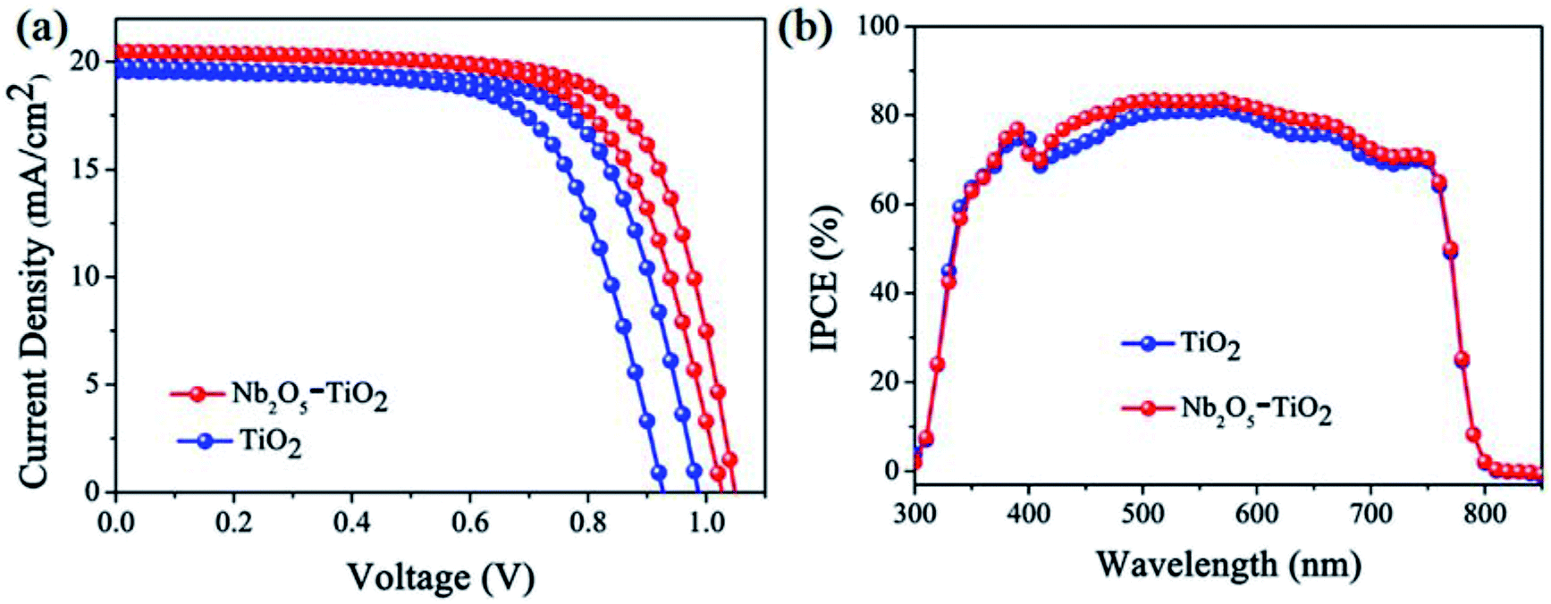 | ||
| Fig. 5 (a) J–V curves and (b) IPCE spectra of the best-performing PSCs made with TiO2 and Nb2O5–TiO2 ETLs on FTO glass. | ||
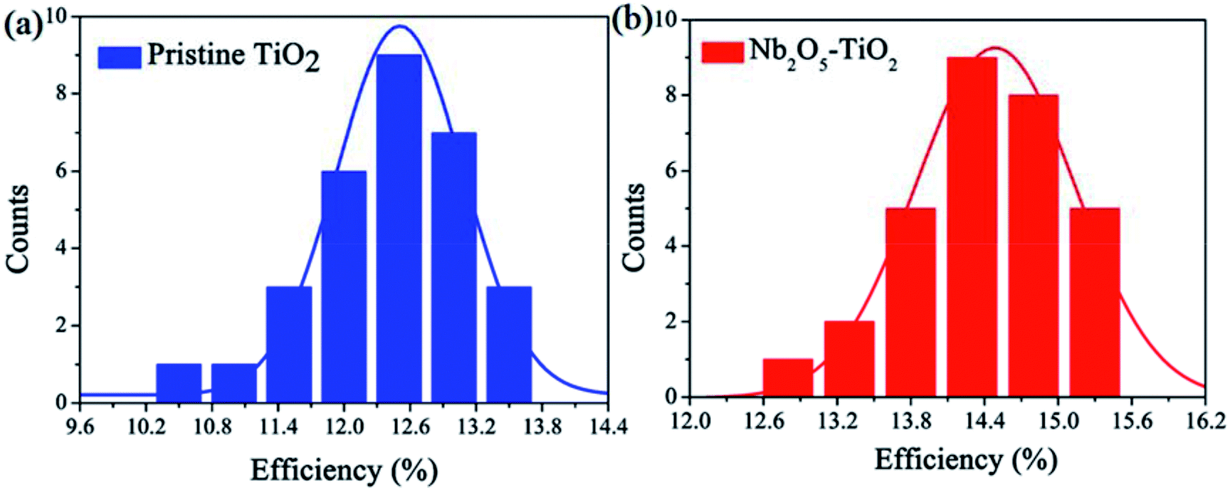 | ||
| Fig. 6 PCE distribution histogram of PSCs based on TiO2 (a) and Nb2O5–TiO2 (b) ETLs. | ||
3.3. Recombination
To gain insight into the electron extraction and transport mechanism, the steady-state PL and TRPL were measured for the perovskite absorber layer deposited on both the ETL-based substrates. Fig. 7a shows that the spectral peak for the FTO/perovskite sample at 766 nm apparently has the highest PL intensity, indicating serious recombination occurring in the sample. The FTO/Nb2O5–TiO2/perovskite sample has the lowest PL intensity, even lower than that of the FTO/TiO2/perovskite sample. Interestingly, compared to the PL peak for the control samples, the peak for the FTO/Nb2O5–TiO2/perovskite film exhibits a considerable blue-shift.40 This suggests that Nb2O5–TiO2 substrate is favorable to obtain higher-quality perovskite films than the control group. Perovskite with higher crystallinity and considerably less trap density than the corresponding bandgap will decrease (i.e., the conduction band minimum will move down).41 Fig. 7b shows the time-resolved photoluminescence (TRPL) decay curves obtained to analyze the PL lifetimes of the perovskite films prepared on both the ETL-based substrates. PL decay transients and the corresponding PL lifetimes were obtained by performing fitting using a bi-exponential decay function, f(t) = A1exp(−t/τ1) + A2exp(−t/τ2), where τ1 is the fast transient component representing the surface properties and τ2 is the slow component resulting from the bulk properties.42,43 The fitted parameters for the glass/perovskite, glass/TiO2/perovskite, and glass/Nb2O5–TiO2/perovskite samples are summarized in Table S2.† For the glass/CH3NH3PbI3 sample, τ1 is 1.05 ns (1.89%) and τ2 is 429.50 ns (98.11%), with an amplitude average lifetime of 49.40 ns. For the TiO2/CH3NH3PbI3 sample, τ1 is 1.36 ns (2.93%) and τ2 is 255.33 ns (97.07%), with an amplitude average lifetime of 39.48 ns. For the Nb2O5–TiO2/CH3NH3PbI3 sample, τ1 is 0.92 ns (11.68%) and τ2 is 223.58 ns (88.32%), with an average lifetime was 7.60 ns. Therefore, it is apparent that the photon-induced electrons transfer from perovskite to the Nb2O5–TiO2 ETL is faster and more effective than that from perovskite to the TiO2 ETL. Thus, the PL characterizations confirm that the large enhancement in the photovoltaic performances of the Nb2O5–TiO2 ETL can be attributed to the enhanced charge extraction.
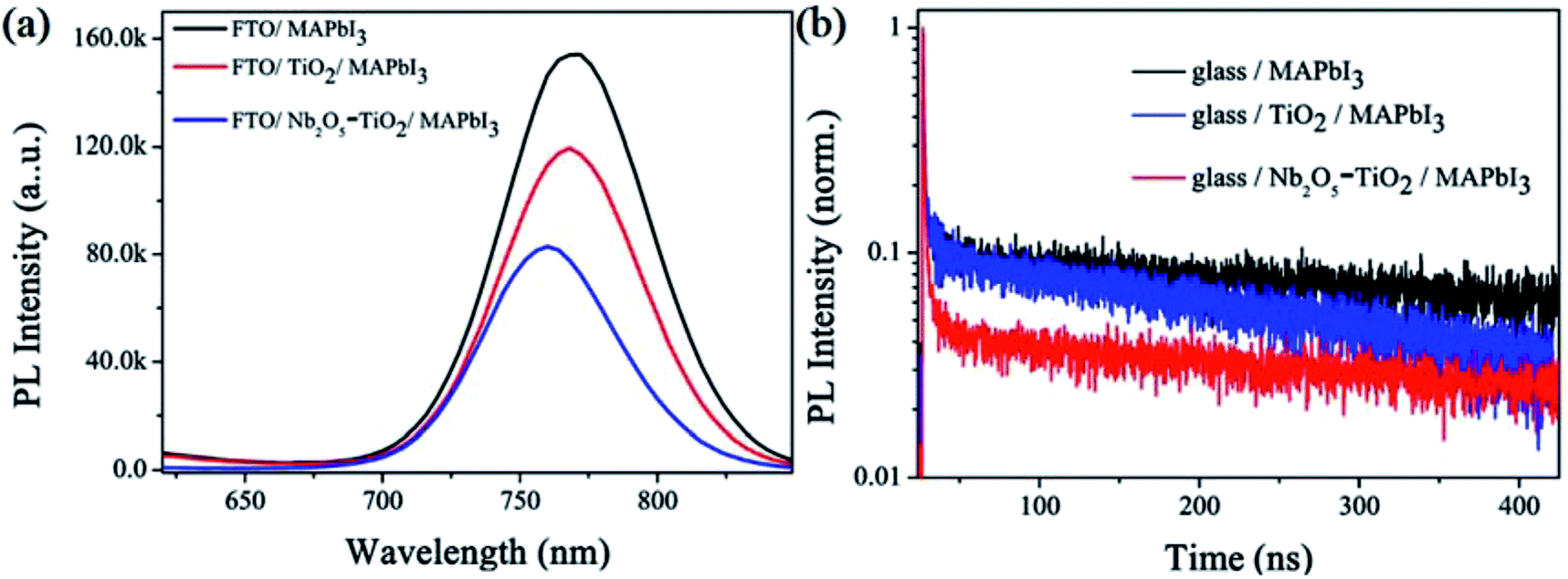 | ||
| Fig. 7 (a) Steady-state photoluminescence (PL) spectra and (b) normalized time-resolved photoluminescence (TRPL) spectra of pristine perovskite and perovskite layers grown on TiO2 and Nb2O5–TiO2 ETLs. | ||
3.4. Flexible perovskite solar cells
The totally room-temperature UV process for efficient ETLs is very suitable for fabricating high-performance flexible PSCs. The excellent performance of uniform and dense Nb2O5–TiO2 ETLs prompted us to fabricate flexible perovskite solar cells using flexible substrates. Nb2O5–TiO2 ETLs were successfully fabricated on indium tin oxide (ITO)/PET substrates, and perovskite, spiro-OMeTAD, and a gold electrode were sequentially deposited using the same methods as those used for the FTO glass-based devices. Fig. 8a shows the J–V curves for the perovskite solar cells fabricated using flexible ITO/PET substrates, and the inset illustrates a photograph of a flexible perovskite solar cell fabricated using flexible ITO/PET substrates. For the flexible device, Jsc is 20.04 mA cm−2, Voc is 0.99 V, and the FF is 0.69, giving the best PCE of 13.60%. The PCE is lower than that of the rigid device because of the decreased Jsc, Voc and FF; the decrease is probably caused by the higher series resistance and lower transmittance of the ITO/PET substrate in the short wavelength spectrum.17 Fig. 8b shows the J–V curves for the flexible device after it is recovered from the given bending radius. The key J–V parameters of the devices are summarized in Table S3.† After the device is bent with R = 10, 5, and 3 mm, the PCE values degenerate to 13.03%, 10.70%, and 3.39%, respectively. As shown in Fig. 8b, the performance of the flexible device does not show serious degradation when the bending radius is 10 mm. When the bending radius is 3 mm, the brittle ITO breaks44 and the PCE is greatly reduced simultaneously, indicating that the flexible devices show good mechanical stability and the Nb2O5–TiO2 ETLs is a promising electron transport material.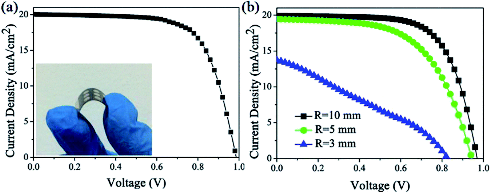 | ||
| Fig. 8 (a) The J–V curves of best PCE of the perovskite solar cells device using flexible PET/ITO substrates. The inset shows the flexible PSC based on Nb2O5–TiO2 ETLs coated on ITO/PET substrate. (b) J–V curves of the flexible PSCs obtained after recovery from bending at various radius (R = 10, 5, and 3 mm). | ||
4. Conclusion
We have demonstrated that Nb2O5–TiO2 is an excellent ETL material for perovskite solar cells, with the champion cell showing a considerably higher PCE (15.25%) than that of devices based on a pristine TiO2 ETL and that of a rigid substrate (13.47%). In the proposed process, niobium ethoxide facilitates the spontaneous coalescence of the TiO2 NCs, thereby forming Nb2O5–TiO2 ETL. Our results suggest that low-temperature solution-processed Nb2O5–TiO2 could be a good ETL candidate for producing efficient perovskite solar cells. Our facile strategy is highly suitable for fabricating high-performance flexible PSCs because it does not need a high-temperature process and can easily modify the ETL via the direct addition of a reagent. This approach will pave the way for further advances in flexible PSCs and is feasible for large scale roll-to-roll processing.Conflicts of interest
There are no conflicts to declare.Acknowledgements
This work was supported by the National Natural Science Foundation of China (Grant No. 51572037, 51335002), the Priority Academic Program Development of Jiangsu Higher Education Institutions and Jiangsu Science and Technology Project (BE2017006-3), the Natural Science Foundation of the Jiangsu Higher Education Institutions of China (Grant No. 14KJA430001).References
- H. P. Zhou, Q. Chen, G. Li, S. Luo, T.-B. Song, H. –S. Duan, Z. R. Hong, J.-B. You, Y. S. Liu and Y. Yang, Interface engineering of highly efficient perovskite solar cells, Science, 2014, 345(6196), 542–546 CrossRef CAS PubMed.
- X. Li, D. Q. Bi, C. Y. Yi, J.-D. Décoppet, J. S. Luo, S. M. Zakeeruddin, A. Hagfeldt and M. Grätzel, A vacuum flash-assisted solution process for high-efficiency large-area perovskite solar cells, Science, 2016, 353(6294), 58–62 CrossRef CAS PubMed.
- Z. Wang, Z. J. Shi, T. T. Li, Y. H. Chen and W. Huang, Stability of Perovskite Solar Cells: A Prospective on the Substitution of the A Cation and X Anion, Angew. Chem., Int. Ed., 2017, 56(5), 1190–1212 CrossRef CAS PubMed.
- H. Tsai, W. Nie, J. C. Blancon, C. C. Stoumpos, R. Asadpour, B. Harutyunyan, A. J. Neukirch, R. Verduzco, J. J. Crochet, S. Tretiak, L. Pedesseau, J. Even, M. A. Alam, G. Gupta, J. Lou, P. M. Ajayan, M. J. Bedzyk and M. G. Kanatzidis, High-efficiency two-dimensional Ruddlesden-Popper perovskite solar cells, Nature, 2016, 536(7616), 312–316 CrossRef CAS PubMed.
- H. Chen, F. Ye, W. T. Tang, J. J. He, M. S. Yin, Y. B. Wang, F. X. Xie, E. B. Bi, X. D. Yang, M. Grätzel and L. Y. Han, A solvent- and vacuum-free route to large-area perovskite films for efficient solar modules, Nature, 2017, 550(7674), 92–95 CAS.
- X. Zhang, X. D. Ren, B. Liu, R. Munir, X. J. Zhu, Y. Dong, J. B. Li, Y. C. Liu, D.-M. Smilgies, R. P. Li, Z. Yang, T. Q. Niu, X. L. Wang, A. Amassian, K. Zhao and S. Z. Liu, Stable high efficiency two-dimensional perovskite solar cells via cesium doping, Energy Environ. Sci., 2017, 10(10), 2095–2102 CAS.
- National Renewable Energy Laboratory (NREL), Best Research-Cell Efficiencies Chart, 2017, http://www.nrel.gov/pv/assets/images/efficiency-chart.png.
- H. Y. Zhang, J. J. Shi, X. Xu, L. F. Zhu, Y. H. Luo, D. M. Li and Q. B. Meng, Mg-doped TiO2 boosts the efficiency of planar perovskite solar cells to exceed 19%, J. Mater. Chem. A, 2016, 4(40), 15383–15389 CAS.
- D. T. Liu, S. B. Li, P. Zhang, Y. F. Wang, R. Zhang, H. Sarvari, F. Wang, J. Wu, Z. M. Wang and Z. D. Chen, Efficient planar heterojunction perovskite solar cells with Li-doped compact TiO2 layer, Nano Energy, 2017, 31, 462–468 CrossRef CAS.
- A. A. Sutanto, S. Lan, C.-F. Cheng, S. B. Mane, H.-P. Wu, M. Leonardus, M.-Y. Xie, S.-C. Yeh, C.-W. Tseng, C.-T. Chen, E. W.-G. Diau and C.-H. Hung, Solvent-assisted crystallization via a delayed-annealing approach for highly efficient hybrid mesoscopic/planar perovskite solar cells, Sol. Energy Mater. Sol. Cells, 2017, 172, 270–276 CrossRef CAS.
- K. Wojciechowski, M. Saliba, T. Leijtens, A. Abatea and H. J. Snaith, Sub-150 °C processed meso-superstructured perovskite solar cells with enhanced efficiency, Energy Environ. Sci., 2014, 7(3), 1142–1147 CAS.
- K. Mahmood, B. S. Swain and H. S. Jung, Controlling the Surface Nanostructure of ZnO and Al-doped ZnO Thin Films Using Electrostatic Spraying for Their Application in 12% Efficient Perovskite Solar Cells, Nanoscale, 2014, 6(15), 9127–9138 RSC.
- W. S. Yang, J. H. Noh, N. J. Jeon, Y. C. Kim, S. C. Ryu, J. W. Seo and S. Seok II, High-performance photovoltaic perovskite layers fabricated through intramolecular exchange, Science, 2015, 348(6240), 1234–1237 CrossRef CAS PubMed.
- L. Xiong, M. Qin, C. Chen, J. Wen, G. Yang, Y. Guo, J. Ma, Q. Zhang, P. Qin, S. Z. Li and G. J. Fang, Fully High-Temperature-Processed SnO2 as Blocking Layer and Scaffold for Efficient, Stable, and Hysteresis-Free Mesoporous Perovskite Solar Cells, Adv. Funct. Mater., 2018, 28(10), 1706276 CrossRef.
- X. Fang, Y. H. Wu, Y. T. Lu, Y. Sun, S. Zhang, J. Zhang, W. H. Zhang, N. Y. Yuan and J. N. Ding, Annealing-free perovskite films based on solvent engineering for efficient solar cells, J. Mater. Chem. C, 2017, 5(4), 842–847 RSC.
- J. P. C. Baena, L. Steier, W. Tress, M. Saliba, S. Neutzner, T. Matsui, F. T. Giordano, J. Jacobsson, A. R. S. Kandada, S. M. Zakeeruddin, A. Petrozza, A. Abate, M. K. Nazeeruddin, M. Grätzel and A. Hagfeldt, Highly efficient planar perovskite solar cells through band alignment engineering, Energy Environ. Sci., 2015, 8(10), 2928–2934 Search PubMed.
- D. Yang, R. X. Yang, J. Zhang, Z. Yang, S. Z. Liu and C. Li, High efficiency flexible perovskite solar cells using superior low temperature TiO2, Energy Environ. Sci., 2015, 8(11), 3208–3214 CAS.
- J. Ma, X. Zheng, H. Lei, W. Ke, C. Chen, Z. Chen, G. Yang and G.-J. Fang, Highly efficient and stable planar perovskite solar cells with large-scale manufacture of e-beam evaporated SnO2 toward commercialization, Solar RRL, 2017, 1(10), 1700118 CrossRef.
- X. Fang, J. N. Ding, N. Y. Yuan, P. Sun, M. H. Lv, G. Q. Ding and C. Zhu, Graphene quantum dot incorporated perovskite films: passivating grain boundaries and facilitating electron extraction, Phys. Chem. Chem. Phys., 2017, 19(8), 6057–6063 RSC.
- L.-L. Gao, C.-X. Li, C.-J. Li and G.-J. Yang, Large-area high-efficiency perovskite solar cells based on perovskite films dried by the multi-flow air knife method in air, J. Mater. Chem. A, 2016, 5(4), 1548–1557 Search PubMed.
- T. Matsui, J.-Y. Seo, M. Saliba, S. M. Zakeeruddin and M. Grätzel, Room-Temperature Formation of Highly Crystalline Multication Perovskites for Efficient, Low-Cost Solar Cells, Adv. Mater., 2017, 29(15), 1606258 CrossRef PubMed.
- X. T. Yin, P. Chen, M. D. Que, Y. L. Xing, W. X. Que, C. M. Niu and J. Y. Shao, Highly Efficient Flexible Perovskite Solar Cells Using Solution-Derived NiOx Hole Contacts, ACS Nano, 2016, 10(3), 3630–3636 CrossRef CAS PubMed.
- G. Yang, C. Chen, F. Yao, Z. Chen, Q. Zhang, X. Zheng, J. Ma, H. Lei, P. Qin, L. Xiong, W. Ke, G. Li, Y. Yan and G. Fang, Effective Carrier-Concentration Tuning of SnO2 Quantum Dot Electron-Selective Layers for High-Performance Planar Perovskite Solar Cells, Adv. Mater., 2018, 1706023, DOI:10.1002/adma.201706023.
- H. Tan, A. Jain, O. Voznyy, X.-Z. Lan, F. P. García de Arquer, J. Z. Fan, R. Quintero-Bermudez, M. J. Yuan, B. Zhang, Y. Zhao, F. Fan, P. Li, L. N. Quan, Y. Zhao, Z.-H. Lu, Z. Yang, S. Hoogland and E. H. Sargent, Efficient and stable solution-processed planar perovskite solar cells via contact passivation, Science, 2017, 355(6326), 722–726 CrossRef CAS PubMed.
- D. Yang, R. Yang, X. Ren, X. Zhu, Z. Yang, C. Li and S. Liu, Hysteresis-Suppressed High-Efficiency Flexible Perovskite Solar Cells Using Solid-State Ionic-Liquids for Effective Electron Transport, Adv. Mater., 2016, 28(26), 5206–5213 CrossRef CAS PubMed.
- C. Yang, Mi. Yu, D. Chen, Y. Zhou, W. Wang, Y. Li, T.-C. Lee and D. Yun, An annealing-free aqueous-processed anatase TiO2 compact layer for efficient planar heterojunction perovskite solar cells, Chem. Commun., 2017, 53(79), 10882–10885 RSC.
- J. P. C. Baena, L. Steier, W. Tress, M. Saliba, S. Neutzner, T. Matsui, F. Giordano, T. J. Jacobsson, A. R. S. Kandada, S. M. Zakeeruddin, A. Petrozza, A. Abate, M. K. Nazeeruddin, M. Grätzel and A. Hagfeldt, Highly Efficient Planar Perovskite Solar Cells through Band Alignment Engineering, Energy Environ. Sci., 2015, 8(10), 2928–2934 Search PubMed.
- X. Ling, J. Yuan, D. Liu, Y. Wang, Y. Zhang, S. Chen, H. Wu, F. Jin, F. Wu, G. Shi, X. Tang, J. Zheng, S. Liu, Z. Liu and W. Ma, Room-Temperature Processed Nb2O5 as the Electron-Transporting Layer for Efficient Planar Perovskite Solar Cells, ACS Appl. Mater. Interfaces, 2017, 9(27), 23181–23188 CAS.
- N. Usha, R. Sivakumar, C. Sanjeeviraja and M. Arivanandhan, Niobium Pentoxide (Nb2O5) Thin Films: Rf Power and Substrate Temperature Induced Changes in Physical Properties, Optik, 2015, 126(19), 1945–1950 CrossRef CAS.
- B.-X. Chen, H.-S. Rao, W.-G. Li, Y.-F. Xu, H.-Y. Chen, D.-B. Kuang and C.-Y. Su, Achieving high-performance planar perovskite solar cell with Nb-doped TiO2 compact layer by enhanced electron injection and efficient charge extraction, J. Mater. Chem. A, 2016, 4(15), 5647–5653 CAS.
- W. Ke, G. Fang, Q. Liu, L. Xiong, P. Qin, H. Tao, J. Wang, H. Lei, B. Li, J. Wan, G. Yang and Y. Yan, Low-Temperature Solution-Processed Tin Oxide as an Alternative Electron Transporting Layer for Efficient Perovskite Solar Cells, J. Am. Chem. Soc., 2015, 137(21), 6730–6733 CrossRef CAS PubMed.
- S. Pisoni, F. Fu, T. Feurer, M. Makha, B. Bissig, S. Nishiwaki, A. N. Tiwari and S. Buecheler, Flexible NIR-transparent perovskite solar cells for all-thin-film tandem photovoltaic devices, J. Mater. Chem. A, 2017, 5(26), 13639–13647 CAS.
- W. Zhang, M. Saliba, D. T. Moore, S. K. Pathak, M. T. Hörantner, T. Stergiopoulos, S. D. Stranks, G. E. Eperon, J. A. Alexander-Webber, A. Abate, A. Sadhanala, S. Yao, Y. Chen, R. H. Friend, L. A. Estroff, U. Wiesner and H. J. Snaith, Ultrasmooth organic–inorganic perovskite thin-film formation and crystallization for efficient planar heterojunction solar cells, Nat. Commun., 2015, 6, 6142 CrossRef CAS PubMed.
- A. M. Goodman and A. Rose, Double Extraction of Uniformly Generated Electron-Hole Pairs from Insulators with Noninjecting Contacts, J. Appl. Phys., 1971, 42(7), 2823–2830 CrossRef CAS.
- C. Goh, R. J. Kline, M. D. McGehee, E. N. Kadnikova and J. M. J. Frechet, Molecular-weight-dependent mobilities in regioregular poly(3-hexyl-thiophene) diodes, Appl. Phys. Lett., 2005, 86(12), 122110 CrossRef.
- D. Yang, X. Zhou, R. Yang, Y. Zhou, Y. Wei, X.-L. Wang, Can Li, S.-Z. Liu and P. H. Chang Robert, Surface optimization to eliminate hysteresis for record efficiency planar perovskite solar cells, Energy Environ. Sci., 2016, 9(10), 3071–3078 CAS.
- Q. Jiang, Z. Chu, P. Wang, X. Yang, H. Liu, Y. Wang, Z. Yin, J. Wu, X. Zhang and J. You, Planar-Structure Perovskite Solar Cells with Efficiency beyond 21%, Adv. Mater., 2017, 29(46), 1703852 CrossRef PubMed.
- G. Yang, H. Lei, H. Tao, X. Zheng, J. Ma, Q. Liu, W. Ke, Z. Chen, L. Xiong, P. Qin, Z. Chen, M. Qin, X. Lu, Y. Yan and G. Fang, Reducing Hysteresis and Enhancing Performance of Perovskite Solar Cells Using Low-Temperature Processed Y-Doped SnO2 Nanosheets as Electron Selective Layers, Small, 2017, 13(2), 1601769 CrossRef PubMed.
- P. Wang, J. Zhao, J. Liu, L. Wei, Z. Liu, L. Guan and G. Cao, Stabilization of organometal halide perovskite films by SnO2 coating with inactive surface hydroxyl groups on ZnO nanorods, J. Power Sources, 2017, 339(30), 51–60 CrossRef CAS.
- Y. Shao, Z. Xiao, C. Bi, Y. Yuan and J. Huang, Origin and elimination of photocurrent hysteresis by fullerene passivation in CH3NH3PbI3 planar heterojunction solar cells, Nat. Commun., 2014, 5, 5784 CrossRef CAS PubMed.
- M. Long, T. Zhang, W. Xu, X. Zeng, F. Xie, Q. Li, Z. Chen, F. Zhou, K. S. Wong, K. Yan and J. Xu, Large-Grain Formamidinium PbI3−xBrx for High-Performance Perovskite Solar Cells via Intermediate Halide Exchange, Adv. Energy Mater., 2017, 7(12), 1601882 CrossRef.
- J. W. Lee, H. S. Kimand and N. G. Park, Lewis Acid-Base Adduct Approach for High Efficiency Perovskite Solar Cells, Acc. Chem. Res., 2016, 49(2), 311–319 CrossRef CAS PubMed.
- Q. Dong, Y. Fang, Y. Shao, P. Mulligan, J. Qiu, L. Cao and J. Huang, Electron-hole diffusion lengths > 175 μm in solution-grown CH3NH3PbI3 single crystals, Science, 2015, 347(6225), 967–970 CrossRef CAS PubMed.
- J. W. Jo, M. Seo, M. Park, J. Kim, J. S. Park, I. K. Han, H. Ahn, J. W. Jung, B.-H. Sohn, M. J. Ko and H. J. Son, Improving Performance and Stability of Flexible Planar-Heterojunction Perovskite Solar Cells Using Polymeric Hole-Transport Material, Adv. Funct. Mater., 2016, 26(25), 4464–4471 CrossRef CAS.
Footnote |
| † Electronic supplementary information (ESI) available. See DOI: 10.1039/c8ra01571f |
| This journal is © The Royal Society of Chemistry 2018 |