DOI:
10.1039/C8RA01481G
(Paper)
RSC Adv., 2018,
8, 13094-13102
Impact of inkjet printed ZnO electron transport layer on the characteristics of polymer solar cells†
Received
16th February 2018
, Accepted 28th March 2018
First published on 9th April 2018
Abstract
In this paper, we demonstrate that zinc oxide (ZnO) layers deposited by inkjet printing (IJP) can be successfully applied to the low-temperature fabrication of efficient inverted polymer solar cells (i-PSCs). The effects of ZnO layers deposited by IJP as electron transport layer (ETL) on the performance of i-PSCs based on PTB7-Th:PC70BM active layers are investigated. The morphology of the ZnO-IJP layers was analysed by AFM, and compared to that of ZnO layers deposited by different techniques. The study shows that the morphology of the ZnO underlayer has a dramatic effect on the band structure and non-geminate recombination kinetics of the active layer deposited on top of it. Charge carrier and transient photovoltage measurements show that non-geminate recombination is governed by deep trap states in devices made from ZnO-IJP while trapping is less significant for other types of ZnO. The power conversion efficiency of the devices made from ZnO-IJP is mostly limited by their slightly lower JSC, resulting from non-optimum photon conversion efficiency in the visible part of the solar spectrum. Despite these minor limitations their J–V characteristics compare very favourably with that of devices made from ZnO layer deposited using different techniques.
Introduction
Polymer solar cells (PSCs) are considered a promising low-cost energy source since they can be produced on large areas on rigid and flexible substrates using low temperature processes.1,2 In the last decade, the performance of PSCs has increased rapidly, mainly due to the development of new polymers with improved light absorption, charge carrier mobility and crystallinity.3–6 As such, efficiencies over 11% have been reported,7,8 however, despite these spectacular figures, stability has not yet matched that of inorganic solar cells. In this respect PSCs with an inverted architecture (i-PSCs) have been shown to be the most promising long-lasting alternative to conventional PSC.9,10 In i-PSCs, a thin film of a metal oxide (MO) (i.e. molybdenum oxide [MoO3], vanadium oxide [V2O5], nickel oxide [NiO] or tungsten oxide [WO3]) is used as hole transport layer (HTL). The MO interlayer provides higher stability and lower ohmic contact resistance than the PEDOT:PSS equivalent in conventional PSCs.11–13 As the electron transport layer (ETL) poly [(9,9-bis(30-(N,N-dimethylamino)propyl)-2,7-fluorene)-alt-2,7-(9,9-dioctylfluorene)] (PFN),4,14,15 zinc oxide (ZnO)16,17 and titanium oxide (TiOx)9,10,18 are commonly used. ZnO has attracted much interest due to its high transparency, high air-stability and high electron mobility. Moreover, ZnO can be easily solution-processed on ITO substrates at room temperature by several coating methods (i.e. spin-coating,19 spray-coating20 and dip-coating.21 Spin-coating is the most commonly used method of deposition as it yields films with relatively high uniformity and well-controlled thickness. Nevertheless, spin-coating is not a compatible method with large-scale continuous process such as roll-to-roll (R2R) processing.22 Inkjet printing (IJP), however is a very promising technique for the large-scale production of i-PSCs and commercialization due to its compatibility with R2R process, the possibility of patterning without any chemical processes (i.e. wet etching of photoresist) and the reduction of material (solution) wasting. As a result, IJP has already been used for the manufacture of organic electronics devices23–25 and several authors have reported ZnO layers deposited by IJP (ZnO-IJP) on thin film transistors,26 micro photodetectors27 and i-PSCs fabrication.28 Despite these recent reports, ZnO deposited by IJP for organic photovoltaic applications have been virtually unexplored to date. Therefore, herein we describe the fabrication and electrical characterization of ZnO-IJP layers as ETL for i-PSCs. The i-PSCs devices were based on active layers composed of PTB7:Th and PC70BM. Similar devices were fabricated with ZnO as ETL deposited by spin coating (ZnO-SC) and thermal evaporation (ZnO-TE) as control. A qualitative charge carrier recombination kinetics analysis was carried out using the charge carrier extraction (CE) and transient photovoltage (TPV) methods. The results of CE/TPV combined with ideality factor analysis demonstrated that recombination kinetics are governed by different mechanisms in IJP-made devices with respect to SC and TE–made devices. Additional impedance spectroscopy (IS) results reveal that devices made from ZnO-IJP exhibit a similar charge transport resistance compared to devices with ZnO-SC, while devices with ZnO-TE show the highest charge transport resistance.
Results and discussion
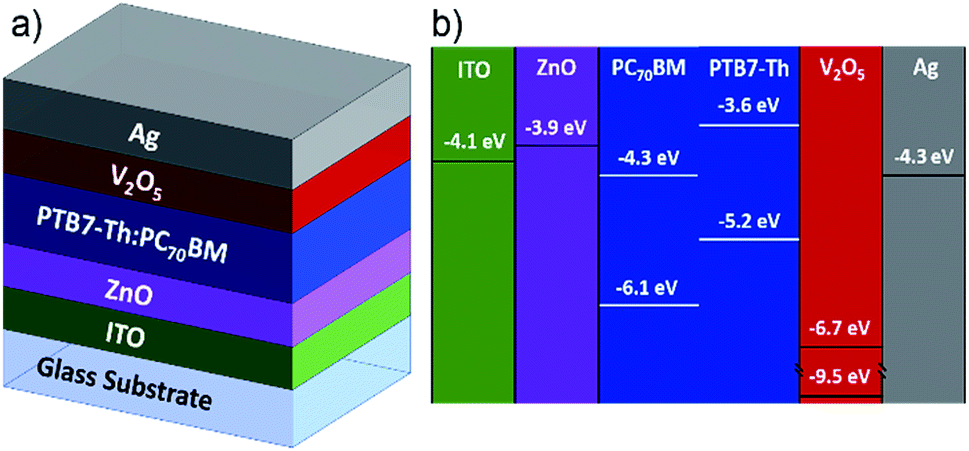
The ZnO-IJP layers were used as ETL in inverted organic solar cells with the architecture ITO/ZnO/PTB7-Th:PC70BM/V2O5/Ag. Fig. 1a shows the architecture of the devices and (1b) shows the energy level diagram for materials used in the devices taken from the literature.4,6,15,29
 |
| | Fig. 1 (a) Inverted architecture of the fabricated devices. (b) Energy level diagram for materials used for device fabrication taken from the literature. | |
Electrical characterisation
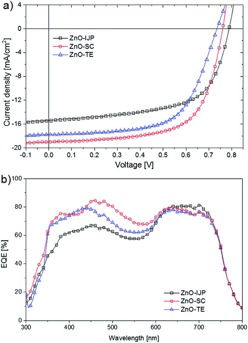
Fig. 2a shows the current density vs. voltage (J–V) characteristics of the best-performing i-PSCs under simulated AM 1.5G illumination (100 mW cm−2). The devices made from ZnO-IJP show a power conversion efficiency (PCE) of 7.47%, a VOC of 0.789 V, a JSC of 15.35 mA cm−2 and a fill factor (FF) of 61.59%. The devices made from ZnO-IJP and ZnO-SC have similar VOC and series resistances (RS), while devices with ZnO-TE have the lowest VOC and highest RS. The PCE of the devices made from ZnO-IJP is ∼20% and ∼9% lower than that of devices with ZnO-SC and ZnO-TE, respectively. All the devices have similar FF. Table 1 summarizes the features of the best-performing devices. The standard deviation for all parameters of i-PSCs was calculated over eight devices and is depicted in parentheses in Table 1. These results are similar to those reported from devices based on PTB7-Th:PC70BM with ZnO as ETL deposited by spin-coating,4,19,30 spray coating20 and sputtering31 techniques. Additionally, all devices reported herein showed to have good reproducibility. A statistical analysis over eight devices was carried out for all i-PSCs and the results are depicted in Fig. S3†. The devices made from ZnO-IJP exhibit somewhat higher dispersion which can be attributed to the non-optimum homogeneity of the ZnO layer. Interestingly, the devices made from ZnO-IJP exhibit higher VOC than that of devices with ZnO-SC and ZnO-TE. However, the trend of JSC is opposite to that of the VOC, where devices made from ZnO-SC show the highest JSC, and those made from ZnO-IJP show the lowest of all. Devices with ZnO-TE exhibit the lowest VOC and a JSC higher than devices with ZnO-IJP. The external quantum efficiency (EQE) of the devices with ZnO deposited by the three different techniques are shown in Fig. 2b. The EQE curves are seen to corroborate the trend observed for the JSC, as seen by the calculated JSC from EQE in Table 1. All the devices exhibit similar spectral response from 600 nm to 800 nm, however the devices made from ZnO-IJP show a significant decrease in photon conversion efficiency from 300 nm to 600 nm with respect to the other devices. This behaviour has been previously observed in i-PSCs when ZnO nanoparticles were used as ETL.16,32 We found that this decrease in EQE is the result of an increase in reflectance together with a slight decrease in absorption of the active layer in the case of the device made from ZnO-IJP (see ESI† for details).
 |
| | Fig. 2 (a) Current density versus voltage (J–V) characteristics of the best-performing i-PSCs under simulated AM 1.5G illumination. (b) EQE spectra of the best-performing device. | |
Table 1 Parameters of i-PSCs devices based on PTB7-Th:PC70BM under 100 mW cm−2 AM1.5G illumination with ZnO-IJP, ZnO-SC and ZnO-TE as ETL
| |
VOC [V] |
JSC [mA cm−2] |
JSC (EQE) [mA cm−2] |
FF [%] |
PCE [%] |
RS [Ω cm2] |
RSh [Ω cm2] |
| ZnO-IJP |
0.789 (0.026) |
15.35 (1.57) |
14.85 |
61.59 (3.56) |
7.47 (0.66) |
2.11 (0.81) |
376 (48) |
| ZnO-SC |
0.761 (0.004) |
18.94 (0.35) |
18.62 |
65.31 (1.41) |
9.42 (0.16) |
1.97 (0.28) |
751 (105) |
| ZnO-TE |
0.737 (0.014) |
17.79 (0.26) |
16.94 |
62.29 (0.52) |
8.17 (0.24) |
8.69 (0.68) |
850 (195) |
Morphological characterisation
To gain understanding on how the morphology of the ZnO affects the properties of the active layers, we carried out an AFM analysis on all three types of ZnO layers. All the films were deposited on ITO-coated glass substrates in identical conditions as in solar cell devices. Topography images (5 × 5 μm and 1 × 1 μm) of ZnO film deposited by IJP (Fig. 3a and d), spin coating (Fig. 3b and e) and thermal evaporation (Fig. 3c and f), were recorded.
 |
| | Fig. 3 AFM (5 × 5 μm) topographical images using tapping mode: (a) ZnO-IJP film, (b) ZnO-SC film and (c) ZnO-TE film. AFM (1 × 1 μm) topographical images using tapping mode: (d) ZnO-IJP film, (e) ZnO-SC film and (f) ZnO-TE film. | |
Table S1† shows the root-mean-square (RMS) roughness and the maximum peak to peak height of each ZnO film. Interestingly, all three deposition techniques lead to very rough surfaces with RMS roughness values over 7 nm for IJP and SC layers. The peak to peak height is higher than 30 nm in all cases (see Table S1†). The evaporated ZnO layer shows a marked granular topography with grains size in the range of 30 nm, while the other two types of ZnO layers show a much less homogenous topography. The ZnO-SC has more of a “mountain and valley”-like aspect, while the ZnO-IJP layer shows clear aggregates of ZnO nanoparticles. Additionally, it should be noted that the ZnO-IJP layer forms an “isle”-like pattern at macroscopic scale, a result of the nozzle-injection process (see micrograph in Fig. S4†). These rather unusual features are likely the cause of the difference in the J–V characteristics observed from the solar cell devices.
Photophysical characterisation
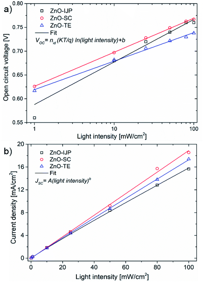
To assess the extent to which the morphology of the ZnO layer affects the energetics of the active layer of the solar cell devices, we carried out a comparative analysis of their ideality factors (nid). To do so, the J–V characteristics of the devices were recorded at different light intensities under simulated AM 1.5G illumination (Fig. S5†). Fig. 4a shows the plot of VOC as a function of the light intensity (LI). In order to calculate the ideality factor (nid), the plot VOC vs. LI was fitted to the eqn (1):| | |
VOC = nid(kT/q)ln(light intensity) + b
| (1) |
where k is the Boltzmann constant, T is the temperature, and q is the elementary charge. The values of nid obtained for devices with ZnO-IJP, ZnO-SC and ZnO-TE were 1.5, 1.2 and 1.0, respectively. These values lie within the range of expected values (1 ≤ nid ≤ 2) for OPV devices. Interestingly, the high value of nid (1.5) of the ZnO-IJP-made devices suggests the presence of a high concentration of deep trap states in the bulk. On the other hand, the devices made from ZnO-SC and ZnO-TE show very low nid. Devices made from ZnO-SC with a nid of 1.2 are in the range of devices in which recombination occurs between a free charge carrier and one carrier trapped in a band tail. For ZnO-TE, the exceptionally low nid, may be evidence of a more tail to tail-like recombination mechanism.33 Fig. 4b shows the plot JSC vs. LI and was fitted to the power law of the form of eqn (2), where b = 0.95, 1.0 and 0.98 for devices with ZnO-IJP, ZnO-SC and ZnO-TE, respectively. These b values indicate that non-geminate recombination is not significant near to short circuit and that no space charge is present.34| | |
JSC = A(light intensity)b
| (2) |
 |
| | Fig. 4 (a) Open circuit voltage as a function of light intensity. The curves were fitted (lines) on the form of eqn 1. (b) Current density as a function of light intensity. The curves were fitted (lines) on the form of eqn (2). | |
To gain more insight on how the band structure affects the J–V characteristics of the devices, particularly the VOC, we carried out a charge carrier recombination kinetics study of the ZnO-based devices, using charge extraction/transient photovoltage techniques (CE/TPV).35–44 The CE measurements allow measuring the average charge density under open circuit conditions.34–36,45,46 Fig. 5a shows the charge carrier density as a function of light bias, resulting in a VOC ranging from 100 to 750 mV. The charge density for all devices close to 1 sun, is in the range of 1016 cm−3, being in good agreement with the reported values for similar organic materials.37 The density of charge in the region from 0.65 V to 0.76 V exhibits an exponential dependency and is related to the accumulated charge within the bulk of the device, analogously to the splitting of the quasi-Fermi levels in intrinsic semiconductors. The curve was fitted using eqn (3) and the γ values for samples are shown in Table 2. The rather low value of γ of devices with ZnO-IJP (4.3) is lower than that expected for ideal semiconductors, an effect that has been attributed to the presence of an exponential tail of trap states extending into the band gap of the active layer. Fig. 5b shows the carrier lifetime (τΔn) as a function of devices' VOC. The curve was fitted using a single exponential decay in the form of eqn (4). The β value for each device is shown in Table 2.
 |
| | Fig. 5 (a) Charge carrier density (n) as a function of the VOC determined from CE measurements. The curves were fitted (lines) on the form of eqn (3). (b) Carrier lifetime (τΔn) as a function of device VOC. For TPV measurements, the transients were induced by a low intensity, pulsed excitation at 650 nm with the devices at open circuit conditions. The curves were fitted (lines) on the form of eqn (4). | |
Table 2 Values of recombination parameters derived from CE/TPV measurements for devices with ZnO layer deposited by IJP, spin coating and thermal evaporation
| Parameter |
ZnO-IJP |
ZnO-SC |
ZnO-TE |
| n0 |
1.6 × 10¹⁵ |
1.4 × 10¹² |
5.8 × 10¹¹ |
| γ |
4.3 |
12.5 |
14.0 |
| β |
12.7 |
18.8 |
23.7 |
| λ |
2.99 |
1.5 |
1.7 |
| ϕ (eqn (6)) |
3.99 |
2.5 |
2.7 |
| ϕ (eqn (7)) |
3.95 |
2.5 |
2.69 |
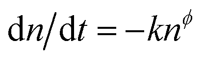
Fig. 6 shows the recombination dynamics of the small perturbation lifetimes combined with the density of charges obtained from CE, allowing determining the overall order of recombination (ϕ) defined by eqn (5), where, ϕ can be calculated using eqn (6) assuming Δn ≪ n in the experimental TPV conditions. The value of ϕ can also be calculated using eqn (7).36 The λ was calculated by fitting the curve τΔn vs. n using eqn (8).
| |
 | (5) |
 |
| | Fig. 6 Carrier lifetime (τΔn) vs. carrier density (n) plot for i-PSCs. The curves were fitted (lines) to a power law decay of the form of eqn (8). | |
The calculated values of λ and ϕ of all devices are summarized in Table 2. The devices made from ZnO-SC and ZnO-TE exhibit similar recombination orders (2.5 and 2.7, respectively), while those from ZnO-IJP-made devices are significantly higher (∼4). Such a high value, as opposed to a value of 2, have been measured several times in earlier reports,33 are to be expected in devices in which recombination is mediated by deep trap states, as corroborated by the high nid. Additionally, the low surface coverage at the macroscopic scale of the ZnO-IJP substrates (see micrograph in Fig. S4†), is consistent with the high ϕ being indicative of significant surface recombination. The low recombination orders measured for the ZnO-SC and ZnO-TE devices are consistent with recombination occurring from traps in the band tails, or with tail to tail-like recombination, as suggested by the extremely low nid. Surface recombination is less significant in these two cases, indicating that the high peak to peak height of the ZnO films does induce a notably lower surface coverage. Most importantly, the significantly slower perturbation lifetimes measured from ZnO-IJP are consistent with the significantly higher VOC observed for these devices with respect to those made from the other two ZnO deposition techniques. The opposite trend is observed between the ZnO-SC and ZnO-TE devices, their relative difference in VOC is, therefore, likely the result of difference in DOS distribution. That is, the device with broader DOS (qualitatively estimated through the parameter γ in the n vs. applied bias plot), i.e. ZnO-SC-made devices, have a higher VOC than ZnO-TE-made devices, despite the fact that their corresponding small perturbation lifetimes are slightly faster that the latter.46–50
In order to quantify the effect of the ZnO-IJP layer on charge transport properties, impedance measurements (IS) were carried out on all the devices at different voltage biases. IS provides valuable information on carrier transport mechanisms involved in the charge extraction on PSCs.15,51–56 Fig. 7 shows the Nyquist plots for ZnO-IJP (a), ZnO-SC (d) and ZnO-TE (g) as ETL taken at different voltages under AM1.5 illumination.
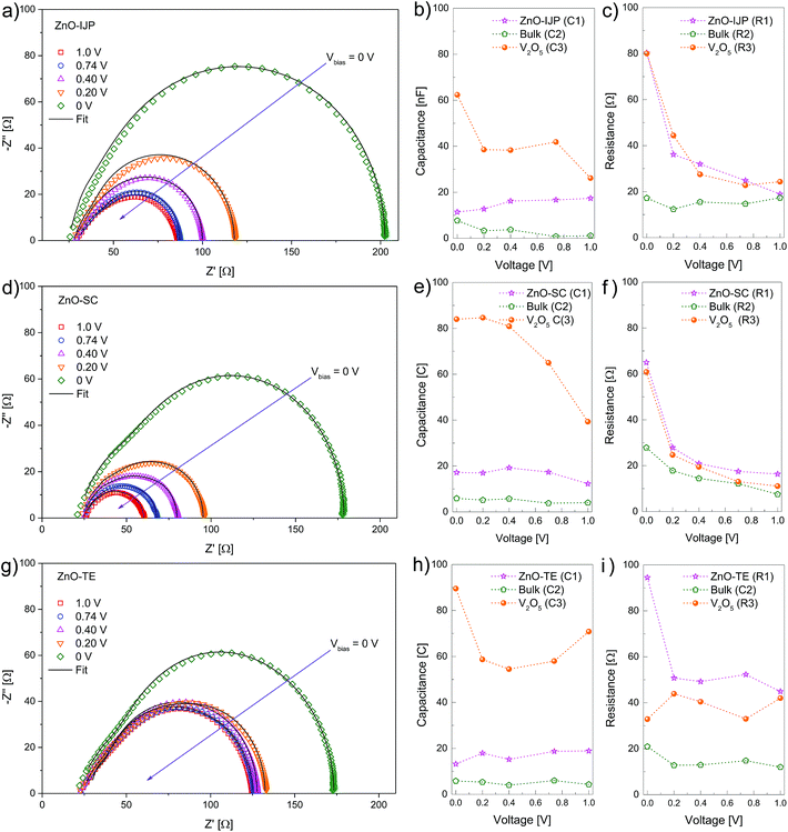 |
| | Fig. 7 Experimental (markers) and fitted (line) IS response for i-PSCs using (a) ZnO-IJP, (d) ZnO-SC and (g) ZnO-TE measured under 1 sun conditions at several applied voltages: 0, 0.2, 0.4, 0.74 and 1 V. Capacitance and resistance data extracted from the fitting of IS measurements for devices using ZnO-IJP (b and c), ZnO-SC (e and f) ZnO-TE (h and i), respectively. | |
The Nyquist plots show mainly one semicircle for all applied voltages (medium frequency from 10 to 1 × 10⁵ Hz), which is associated with charge transfer at the electrode/active layer interface.57 The experimental impedance spectra were fitted using an equivalent electrical model with three resistor/capacitor circuits (3RC) in series15,54,58 (Fig. S6†). Each element of the circuit is associated with the capacitance and resistance of the three different layers of the i-PSC devices.15,55,57 The fitting was performed in Matlab (R2014a) using custom computational methods and literature algorithms,59 yielding R and C values for the different applied voltage biases.
The capacitances of the three RC circuit at the different applied voltages were calculated from the fitting of the IS measurements of devices made from ZnO-IJP, ZnO-SC and ZnO-TE (Fig. 7b, e and h, respectively). The capacitances were linked to the layers involved in the charge transport process by the theoretical capacitance calculation using the equation:
| |
 | (9) |
where,
ε0 is the vacuum dielectric permittivity,
εlayer is the relative dielectric permittivity for each layer:
εbulk,
εZnO and
εV2O5, and
d is the thickness of each layer:
dbulk,
dZnO and
dV2O5. The values used for calculating the capacitance of each layer by
eqn (9) are shown in Table S2
†. Thereby, we related capacitance C1 to the ZnO ETL, C2 to the bulk (active layer) and C3 to the V
2O
5 HTL as shown in
Fig. 7b, e and h. Since C1, C2 and C3 are a component of the RC circuits, the three associated resistances were related to each layer as shown in
Fig. 7c, f and i. The resistances values of ZnO and V
2O
5 layers are similar in i-PSCs with ZnO-IJP and ZnO-SC. In both devices, the resistance of ZnO and V
2O
5 layers decreases as the applied voltage increases. The resistances of ZnO and V
2O
5 layers decrease from ∼80 Ω (ZnO-IJP) and ∼60 Ω (ZnO-SC) at 0 V to ∼20 Ω at 1 V. These high values of resistance at low voltages (from 0 V to 0.2 V) suggest that shunt resistance losses are mainly caused by the hole- and electron-transport layers. In devices with ZnO-TE the resistances of V
2O
5 is lower than that of ZnO. Moreover, at high voltages (from 0.7 V to 1 V) the ZnO and V
2O
5 layers of i-PSCs with ZnO-IJP and ZnO-SC exhibit lower resistance values that of devices with ZnO-TE. These results corroborate the values of series resistances of the devices calculated from
J–
V characteristics.
Discussion and conclusion
In this work, we investigated the use of an inkjet printed ZnO layer as ETL in i-PSCs based on PTB7-Th:PC70BM. The i-PSCs devices showed a maximum power conversion efficiency of 7.47%, which compares very favourably to that obtained on similar i-PSCs using spin coated and thermally evaporated ZnO layers. Combined results from ideality factor and non-geminate recombination studies has brought substantial evidence of a modification of the band structure properties of the active layer, triggered by the ZnO type of underlayer the active layer is deposited on to. As such, the active layer deposited on top of ZnO-IJP shows a higher density of deep trap states, than those deposited on top of ZnO-SC and ZnO-TE. The difference in band structure energetics and recombination dynamics has been shown to follow the trend in VOC measured experimentally from the three types of devices.
Additional impedance spectroscopy measurements have demonstrated that electron injection and extraction have an impact on the shunt and series resistances of the ZnO-IJP-made and ZnO-TE-made devices, thus lowering the FF of both devices slightly. Interestingly, the main parameter limiting the PCE of the ZnO-IJP devices with respect to its spin coated and thermally evaporated counterparts is the lower JSC, which is to some extent the result of a lower spectral photon conversion efficiency in the visible range of the solar spectrum. This effect, was shown to be due to an increase in reflectance together with a slight decrease in absorption of the active layer. Importantly, the morphological aspects of the ZnO layer are not seen to induce an increase in recombination kinetics. On the contrary the higher VOC of ZnO-IJP is the result of slower recombination kinetics with respect to the other two deposition techniques. All in all, this study demonstrates that the ZnO-IJP layer deposited by inkjet printing can be successfully used for the fabrication of highly efficient i-PSCs on a large scale. Work is currently under way to improve the homogeneity of the surface coverage of the substrate in order to maximize the spectral response of the devices.
Experimental section
Materials
Patterned indium thin oxide (ITO)-coated glass substrates with 10 Ω □−1 were acquired from PsiOTec Ltd. The vanadium oxide (V2O5) and chlorobenzene [C6H5Cl] were purchased from Sigma-Aldrich. The zinc oxide (ZnO) nanoparticle ink (crystalline ZnO dispersed in isopropanol and propylene glycol, 2.5 wt%) was purchased from Sigma-Aldrich (808202). Diiodoctane was acquired from Alfa Aesar. Poly[4,8-bis(5-(2-ethylhexyl)thiophen-2-yl)benzo[1,2-b;4,5-b′] dithiophene-2,6-diyl-alt-(4-(2-ethylhexyl)-3-fluorothieno[3,4-b]thiophene-)-2-carboxylate-2-6-diyl)] (PTB7-Th) material was purchased from One-material (One Materials, Inc. Canada). [6,6]-phenyl-C71-butyric acid methyl (PC70BM) was purchased from Solenne BV and silver (Ag, 99.99% purity) was acquired from Testbourne Ltd. All materials were used as received.
ZnO layer deposition
Inkjet printing. First, the ZnO nanoparticle ink (ZnO-ink) with a viscosity of about 8–14 cp and nanoparticle size around 8–16 nm was sonicated during 10 min and was filtered through 0.2 μm PTFE filter. The ZnO-ink was deposited on patterned ITO-coated glass substrate using a DIMATIX DMP-2800 printer. The printing parameters are as follows: drop spacing of 10 μm, drop velocity of 8 m s−1, 15 nozzles at 16 V and jetting frequency of 5 kHz. Subsequently, the samples were sintered at 115 °C during 10 min in air into a conventional oven.
Spin coating. The ZnO precursor was prepared by dissolving zinc acetate dihydrate (Zn(CH3COO))2·2H2O 0.68 M and ethanolamine 0.46 M in 2-methoxyethanol (CH3OCH2CH2OH) and leaving them under vigorous stirring for 1 h at 70 °C. Subsequently, the precursor solution of ZnO was diluted in methanol in 1![[thin space (1/6-em)]](https://www.rsc.org/images/entities/char_2009.gif) :1 ratio. This solution was spin coated on pre-cleaned ITO substrate at 3000 rpm for 30 s. The resulting ZnO film was heated at 110 °C for 1 h in air.
:1 ratio. This solution was spin coated on pre-cleaned ITO substrate at 3000 rpm for 30 s. The resulting ZnO film was heated at 110 °C for 1 h in air.
Evaporation. The ITO substrates were transferred to a high vacuum chamber and 45 nm of ZnO were thermally evaporated at 9 × 10⁻⁷ mbar with an evaporation rate ranging from 0.04 to 0.08 nm s−1.
Solar cells fabrication. The solar cells were fabricated on indium tin oxide (ITO) patterned glass substrates. The ITO substrates (10 Ω □−1) were cleaned in acetone, ethanol and isopropanol using an ultrasonic bath. Subsequently, ITO was dried at 100 °C followed by UV-ozone treatment. Subsequently, the ITO substrates were coated with ZnO (∼40 nm) by either inkjet printing, spin coating or thermal evaporation as described above. The blend solution was prepared by dissolving PTB7-Th and PC70BM (1:1.5 w/w) in chlorobenzene and 1,8-diiodooctane (97:3 by volume) with a concentration of 25 mg mL−1. The blend solution was left stirring overnight, and further aged for 48 h in the dark under nitrogen atmosphere. The blend solution was spin-coated on top of the ZnO interlayer at 800 rpm for 30 s to obtain an active layer 100 nm-thick. The samples were transferred to a vacuum chamber and 5 nm of V2O5 and 100 nm of Ag were deposited by thermal evaporation on top of the active layer at 8 × 10⁻⁷ mbar. The active area for all devices was 0.09 cm2.
Photovoltaics measurements. All current–density vs. voltage (J–V) characteristics were performed at room temperature with a solar simulator (Abet Technologies model 11000 class type A, Xenon arc) and a Keithley 2400 Source-Measure Unit. The light intensity was calibrated by a NREL certified monocrystalline silicon photodiode.
Atomic force microscopy measurements. Atomic force microscopy (AFM) of the samples was performed in tapping mode on a Molecular Imaging model Pico SPM II (pico+). Images were collected in air using silicon probes with typical spring constant of 1–5 nN m−1 and at resonant frequency of 75 kHz.
Photophysical measurements. The charge extractions measurements were carried out in open circuit voltage equilibrium by illuminating the devices using a white light LED ring from LUXEON® Lumileds. Devices are connected to a DC power supply and a function generator TGP110. The light is turned off and the circuit closed to force the charge to pass through an oscilloscope TDS 2022 from Tektronix. In this step, the drop in voltage across a resistance of 50 ohms is recorded by the oscilloscope.In TPV measurements, the background illumination was provided by a ring of 6 white LED's from LUXEON®, while samples are connected to 1 MΩ input terminal of an oscilloscope Tektronix© TDS2022. The small perturbation was applied by a light pulse excited at 650 nm (N2 laser, <100 ns pulses) with a range intensity from 0.1 sun to 1 sun.
Impedance spectroscopy measurements. Impedance spectroscopy was performed using a HP-4192A impedance analyser. Several voltage perturbations (0, 0.2, 0.4, 0.74 and 1 V) were applied at frequency range from 1 kHz to 1 MHz with an AC signal and 15 mV amplitude. The IS measurements were carried out under AM1.5 illumination calibrated by a certified monocrystalline silicon photodiode.
Conflicts of interest
The authors declare no conflict of interest.
Acknowledgements
This work was supported by the Spanish Ministry of Economy, Industry and Competitiveness (MEIC) for grant numbers, TEC2015-71915-REDT and TEC2015-71324-R (MINECO/FEDER), by the ICREA for the ICREA Academia Award, by the Catalan authority for project AGAUR 2017 SGR 1527 and the CONACYT Project 237213 in Mexico. V. S. Balderrama, S. I. Garduño and E. Osorio acknowledge the support received from the Project “Cátedras CONACYT para Jóvenes Investigadores”. The authors thank Dr Daniel Fernandez Pinto for his help on the CE/TPV data analysis. We thank Prof. Emilio Palomares for helpful discussions.
References
- G. Dennler, M. C. Scharber and C. J. Brabec, Adv. Mater., 2009, 21(13), 1323–1338 CrossRef CAS.
- G. Li, R. Zhu and Y. Yang, Nat. Photonics, 2012, 6(3), 153–161 CrossRef CAS.
- V. S. Balderrama, M. Estrada, P. L. Han, P. Granero, J. Pallarès, J. Ferré-Borrull and L. F. Marsal, Sol. Energy Mater. Sol. Cells, 2014, 125, 155–163 CrossRef CAS.
- Z. He, C. Zhong, S. Su, M. Xu, H. Wu and Y. Cao, Nat. Photonics, 2012, 6(9), 593–597 CrossRef CAS.
- Y. Liu, J. Zhao, Z. Li1, C. Mu, W. Ma, H. Hu, K. Jiang, H. Lin, H. Ade and H. Yan, Nat. Commun., 2014, 5(5293), 9 Search PubMed.
- S. H. Liao, H. J. Jhuo, P. N. Yeh, Y. S. Cheng, Y. L. Li, Y. H. Lee, S. Sharma and S. A. Chen, Sci. Rep., 2015, 4(1), 6813 CrossRef PubMed.
- J. Zhao, Y. Li, G. Yang, K. Jiang, H. Lin, H. Ade, W. Ma and H. Yan, Nat. Energy, 2016, 1(2), 15027 CrossRef CAS.
- M. A. Green, Y. Hishikawa, W. Warta, E. Dunlop, D. Levi, J. Hohl-Ebinger and A. Ho-Baillie, Prog. Photovolt: Res. Appl., 2017, 25(7), 668–676 CrossRef.
- J. G. Sánchez, V. S. Balderrama, M. Estrada, E. Osorio, J. Ferré-Borrull, L. F. Marsal and J. Pallarès, Sol. Energy, 2017, 150, 147–155 CrossRef.
- Z. Yin, Q. Zheng, S.-C. Chen, J. Li, D. Cai, Y. Ma and J. Wei, Nano Res., 2015, 8(2), 456–468 CrossRef CAS.
- Z. Yin, J. Wei and Q. Zheng, Adv. Sci., 2016, 3(8), 1–37 Search PubMed.
- S. Chen, J. R. Manders, S. W. Tsang and F. So, J. Mater. Chem., 2012, 22(46), 24202 RSC.
- M. T. Greiner, M. G. Helander, W. M. Tang, Z. B. Wang, J. Qiu and Z. H. Lu, Nat. Mater., 2011, 11(1), 76–81 CrossRef PubMed.
- V. S. Balderrama, F. Ávila-Herrera, J. G. Sánchez, J. Pallarès, O. Vigil-Galán, L. F. Marsal and M. Estrada, IEEE Journal of Photovoltaics, 2016, 6(2), 491–497 CrossRef.
- R. C. I. MacKenzie, V. S. Balderrama, S. Schmeisser, R. Stoof, S. Greedy, J. Pallarès, L. F. Marsal, A. Chanaewa and E. von Hauff, Adv. Energy Mater., 2016, 6(4), 1501742 CrossRef.
- D. Lee, T. Kang, Y. Choi and S. Oh, J. Phys. Chem. Solids, 2017, 105, 66–71 CrossRef CAS.
- X. Zhang, S. Yang, S. Bi, A. Kumaresan, J. Zhou, J. Seifter, H. Mi, Y. Xu, Y. Zhang and H. Zhou, RSC Adv., 2017, 7(20), 12400–12406 RSC.
- G. Kim, J. Kong, J. Kim, H. Kang, H. Back, H. Kim and K. Lee, Adv. Energy Mater., 2015, 5(3), 21–23 Search PubMed.
- R. Kang, Y. J. Noh, J. M. Yun, H. Kim, N. Myoung, E. H. Lee, T. W. Kim, S. I. Na and S. H. Oh, RSC Adv., 2017, 7(43), 26689–26696 RSC.
- D. Zheng, W. Huang, P. Fan, Y. Zheng, J. Huang and J. Yu, ACS Appl. Mater. Interfaces, 2017, 9(5), 4898–4907 CAS.
- A. M. Peiró, P. Ravirajan, K. Govender, D. S. Boyle, P. O'Brien, D. D. C. Bradley, J. Nelson and J. R. Durrant, J. Mater. Chem., 2006, 16(21), 2088–2096 RSC.
- R. Søndergaard, M. Hösel, D. Angmo, T. T. Larsen-Olsen and F. C. Krebs, Mater. Today, 2012, 15(1), 36–49 CrossRef.
- M. Singh, H. M. Haverinen, P. Dhagat and G. E. Jabbour, Adv. Mater., 2010, 22(6), 673–685 CrossRef CAS PubMed.
- T. M. Eggenhuisen, Y. Galagan, A. F. K. V. Biezemans, T. M. W. L. Slaats, W. P. Voorthuijzen, S. Kommeren, S. Shanmugam, J. P. Teunissen, A. Hadipour, W. J. H. Verhees, S. C. Veenstra, M. J. J. Coenen, J. Gilot, R. Andriessen and W. A. Groen, J. Mater. Chem. A, 2015, 3(14), 7255–7262 CAS.
- F. Villani, P. Vacca, G. Nenna, O. Valentino, G. Burrasca, T. Fasolino, C. Minarini and D. della Sala, J. Phys. Chem. C, 2009, 113(30), 13398–13402 CAS.
- S. C. Lim, J. B. Koo, C. W. Park, S. W. Jung, B. S. Na, S. S. Lee and H. Y. Chu, Jpn. J. Appl. Phys., 2014, 53(5S3), 05HB10 CrossRef.
- V. T. Tran, Y. Wei, H. Yang, Z. Zhan and H. Du, Nanotechnology, 2017, 28(9), 95204 CrossRef PubMed.
- A. Singh, S. K. Gupta and A. Garg, Org. Electron., 2016, 35, 118–127 CrossRef CAS.
- Sigma-Aldrich. ZnO nanoparticle ink. Information obtained from sigma-Aldrich: http://www.sigmaaldrich.com/catalog/product/aldrich/793361?lang=es%26region=ES.
- S. H. Liao, H. J. Jhuo, Y. S. Cheng and S. A. Chen, Adv. Mater., 2013, 25(34), 4766–4771 CrossRef CAS PubMed.
- P. Lv, S. C. Chen, Q. Zheng, F. Huang and K. Ding, Appl. Phys. Lett., 2015, 106(16), 163902 CrossRef.
- S. Oh, T. Kang and S. G. Oh, Sol. Energy, 2015, 120, 363–369 CrossRef CAS.
- T. Kirchartz and J. Nelson, Phys. Rev. B, 2012, 86(16), 1–12 CrossRef.
- D. Credgington, Y. Kim, J. Labram, T. D. Anthopoulos and J. R. Durrant, J. Phys. Chem. Lett., 2011, 2, 2759–2763 CrossRef CAS.
- D. Credgington and J. R. Durrant, J. Phys. Chem. Lett., 2012, 3(11), 1465–1478 CrossRef CAS PubMed.
- A. Maurano, C. G. Shuttle, R. Hamilton, A. M. Ballantyne, J. Nelson, W. Zhang, M. Heeney and J. R. Durrant, J. Phys. Chem. C, 2011, 115, 5947–5957 CAS.
- T. M. Clarke, A. Ballantyne, S. Shoaee, Y. W. Soon, W. Duffy, M. Heeney, I. McCulloch, J. Nelson and J. R. Durrant, Adv. Mater., 2010, 46(22), 5287–5291 CrossRef PubMed.
- T. M. Clarke and J. R. Durrant, Chem. Rev., 2010, 11(110), 6736–6767 CrossRef PubMed.
- D. Credgington, R. Hamilton, P. Atienzar, J. Nelson and J. R. Durrant, Adv. Funct. Mater., 2011, 14(21), 2744–2753 CrossRef.
- A. Maurano, R. Hamilton, C. G. Shuttle, A. M. Ballantyne, J. Nelson, B. O'Regan, W. Zhang, I. McCulloch, H. Azimi, M. Morana, C. J. Brabec and J. R. Durrant, Adv. Mater., 2010, 44(22), 4987 CrossRef PubMed.
- R. Shivanna, S. Shoaee, S. Dimitrov, S. K. Kandappa, S. Rajaram, J. R. Durrant and K. S. Narayan, Energy Environ. Sci., 2014, 1(7), 435–441 Search PubMed.
- C. G. Shuttle, R. Hamilton, B. C. O'Regan, J. Nelson and J. R. Durrant, Proc. Natl. Acad. Sci. U. S. A., 2010, 38(107), 16448–16452 CrossRef PubMed.
- C. G. Shuttle, A. Maurano, R. Hamilton, B. O'Regan, J. C. de Mello and J. R. Durrant, Appl. Phys. Lett., 2008, 18(93), 183501–183503 CrossRef.
- C. G. Shuttle, B. O'Regan, A. M. Ballantyne, J. Nelson, D. D. C. Bradley and J. R. Durrant, Phys. Rev. B: Condens. Matter Mater. Phys., 2008, 11(78), 113201 CrossRef.
- P. L. Han, A. Viterisi, J. Ferre-Borrull, J. Pallarés and L. F. Marsal, Org. Electron., 2017, 41, 229–236 CrossRef CAS.
- D. Fernandez, A. Viterisi, V. Challuri, J. W. Ryan, E. Martinez-Ferrero, F. Gispert-Guirado, M. Martinez, E. Escudero, C. Stenta, L. F. Marsal and E. Palomares, ChemSusChem, 2017, 10(15), 3118–3134 CrossRef CAS PubMed.
- A. Sánchez-Díaz, M. Izquierdo, S. Filippone, N. Martin and E. Palomares, Adv. Funct. Mater., 2010, 16(20), 2695–2700 CrossRef.
- G. Garcia-Belmonte, P. P. Boix, J. Bisquert, M. Lenes, H. J. Bolink, A. La Rosa, S. Filippone and N. Martin, J. Phys. Chem. Lett., 2010, 17(1), 2566–2571 CrossRef.
- D. Fernandez, A. Viterisi, J. William Ryan, F. Gispert-Guirado, S. Vidal, S. Filippone, N. Martin and E. Palomares, Nanoscale, 2014, 11(6), 5871–5878 RSC.
- I. Etxebarria, A. Guerrero, J. Albero, G. Garcia-Belmonte, E. Palomares and R. Pacios, Org. Electron., 2014, 11(15), 2756–2762 CrossRef.
- E. Barsoukov and J. R. MacDonald, Impedance Spectroscopy: Theory, Experiment, and Applications, Wiley-Interscience, 2005 Search PubMed.
- G. Garcia-Belmonte, P. P. Boix, J. Bisquet, M. Sessolo and H. J. Bolink, Sol. Energy Mater. Sol. Cells, 2010, 94, 366–375 CrossRef CAS.
- G. García-Belmonte, A. Munar, E. M. Barea, J. Bisquert, I. Ugarte and R. Pacios, Org. Electron., 2008, 9, 847–851 CrossRef.
- A. Guerrero, N. F. Montcada, J. Ajuria, I. Etxebarria, R. Pacios, G. García-Belmonte and E. Palomares, J. Mater. Chem. A, 2013, 1, 12345–12354 CAS.
- B. Ecker, H. J. Egelhaaf, R. Steim, J. Parisi and E. von Hauff, J. Phys. Chem. C, 2012, 116(31), 16333–16337 CAS.
- B. Ecker, J. C. Nolasco, J. Pallarés, L. F. Marsal, J. Posdorfer, J. Parisi and E. von Hauff, Adv. Funct. Mater., 2011, 21, 2705–2711 CrossRef CAS.
- M. S. Suresh, Sol. Energy Mater. Sol. Cells, 1996, 43, 21–28 CrossRef CAS.
- E. Osorio, J. G. Sánchez, L. N. Acquaroli, M. Pacio, J. Ferré-Borrull, J. Pallarés and L. F. Marsal, ACS Omega, 2017, 2(7), 3091–3097 CrossRef CAS.
- W. H. Press, S. A. Teukolsky, W. T. Vettering and B. P. Flannery, Numerical Recipes in C: The Art of Scientific Computing, 2nd edn, Cambridge University Press, 1994 Search PubMed.
Footnote |
| † Electronic supplementary information (ESI) available. See DOI: 10.1039/c8ra01481g |
|
| This journal is © The Royal Society of Chemistry 2018 |
Click here to see how this site uses Cookies. View our privacy policy here. 
 Open Access Article
 This Open Access Article is licensed under a Creative Commons Attribution-Non Commercial 3.0 Unported Licence
 d,
Aurelien Viterisi
d,
Aurelien Viterisi