
 Open Access Article
 This Open Access Article is licensed under a Creative Commons Attribution-Non Commercial 3.0 Unported Licence
Switching the optical and electrical properties of carbon nanotube hybrid films using a photoresponsive dispersant as a dopant†
H. Jintoku ,
Y. Matsuzawa* and
M. Yoshida
,
Y. Matsuzawa* and
M. Yoshida
Research Institute for Sustainable Chemistry, National Institute of Advanced Industrial Science and Technology (AIST), Central 5-2, 1-1-1 Higashi, Tsukuba 305-8565, Japan. E-mail: yoko-matsuzawa@aist.go.jp
First published on 20th March 2018
Abstract
The light-induced switching of the optical and electrical properties of single-walled carbon nanotubes (SWCNTs) was demonstrated following hybridisation with an azobenzene-based photoresponsive dispersant in solid film. The resultant SWCNT/photoresponsive dispersant hybrid film showed switching of absorbance in the near-infrared region by the irradiation of UV and visible lights, which was caused by the change of the doping ability of the dispersant to SWCNT. In addition, the switching of the electrical properties of the SWCNT hybrid film was also observed.
Introduction
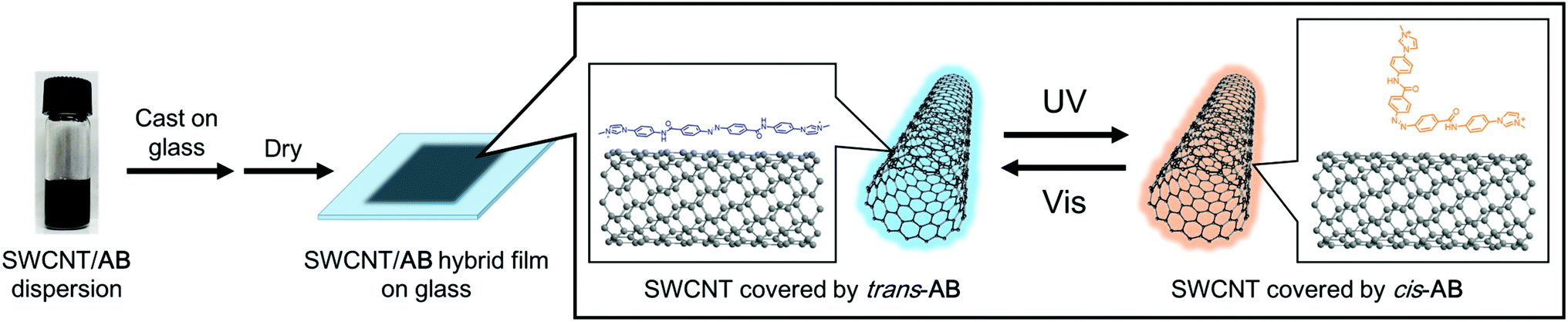
Carbon nanomaterials like single-walled carbon nanotubes (SWCNTs) and graphene are promising candidates in numerous applications such as electronics,1–4 optical devices,5,6 and nanocomposites7–10 because of their extraordinary properties. Recently, stimuli-responsive carbon nanomaterial hybrids have attracted considerable interest because they adopt the exceptional features of carbon nanomaterials with readily available stimuli. Among the various stimuli accessible, light is characteristic because of its high temporospatial resolution, its eco-friendliness, and the wide selection of possible wavelengths. Hybrids of carbon nanomaterials and photoresponsive compounds have great potential applications as sensors,11 memory devices,12 electrical devices,13–16 and storage for solar thermal energy.17–19 In fact, various types of photoactive carbon nanomaterials have been reported, with light being used most often to induce switching of the electrical conductivity of nanocarbon devices. For example, azobenzene-immobilised SWCNTs and graphene have been shown to exhibit switching of their electrical conductivity by UV and visible light irradiation, which may prove useful in memory and sensor devices.14,20 In another example, photoresponsive field-effect transistor devices were demonstrated using spiropyran-immobilised graphene.21In our previous work, we reported a photoresponsive dispersant that can disperse carbon nanomaterials into water and organic solvent.22–25 Moreover, upon irradiation by UV and visible light, the dispersibility of these carbon nanomaterials can be switched between dispersive and precipitative states based on the photoisomerisation of the dispersant.23 In this study, the bulky tetra-ammonium cationic moiety of the photoresponsive dispersant was replaced with an imidazole moiety, giving rise to a greatly enhanced planarity of the entire molecule that is much higher than that of previously reported dispersants. The present work demonstrates novel photoactive carbon nanomaterials using SWCNTs and an azobenzene-based dispersant with a planer structure (AB, Scheme 1). The SWCNT/AB hybrid was obtained by a simple wet-coating method from a uniform dispersion of SWCNT/AB. Interestingly, the SWCNT/AB hybrid film shows not only electrical conductivity switching but also switching of its near-infrared (NIR) absorbance with irradiation of UV and visible light. Notably, these unique switching properties may lead to innovative applications in optoelectronic devices which can input UV and output both NIR and electric signals (e.g. sensor, memory, optical detector, and optical filter).
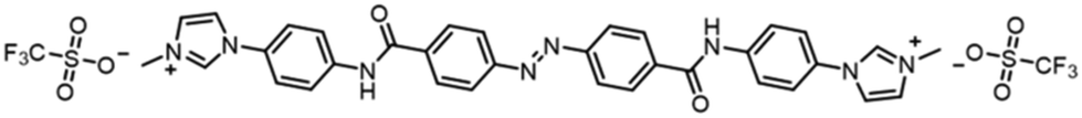 | ||
| Scheme 1 Chemical structure of the azobenzene-derived cation with the trifluoromethanesulfonyl anion (AB). | ||
Experimental
Materials and instruments
The reagents and solvents were purchased from Aldrich, Wako Pure Chemical Industries Ltd., and Tokyo Chemical Industry. Single-walled carbon nanotubes (SWCNT), which were synthesised from a high-pressure carbon monoxide method (HiPco), were purchased from NanoIntegris (d = 0.8–1.2 nm, length = 100–1000 nm).UV-Vis-NIR spectra were measured with a V-670 spectrometer (Jasco) using quartz cells (pass length = 0.5 mm). UV light was irradiated by a UV-LED (EXECURE H-1VH4-V1, HOYA Candeo Optronics) and Super-high pressure mercury lamp (USHIO, E016 with optical cut filter). Atomic Force Microscope (AFM) images (tapping mode) were recorded using an Innova (Veeco Instruments, Inc.) with a Si probe (RTESP-300, f0 = 300 kHz, Bruker). Sheet resistance was measured with a Loresta-AX resistivity meter (MCP-T370, Mitsubishi Chemical Analytech). Raman spectroscopy was measured by an NRS-1000 spectrometer (Jasco) with a 532 nm laser source (2.5 mW). Elemental analysis was recorded using vario MICRO cube (Elementar).
Synthesis of photoresponsive dispersant AB
4-(1H-Imidazol-1-yl)aniline (1.5 g, 9.4 mmol) and triethylamine (2.0 g, 19.8 mmol) dissolved dichloromethane (dehydrated, 20 mL) was added to a solution of 4,4′-azodibenzoyl dichloride (1.0 g, 3.3 mmol) in dichloromethane (dehydrated, 30 mL). The mixture was stirred for 12 h at 25 °C. The precipitates was filtered, washed with dichloromethane, and dried in vacuo, to give 1 (1.7 g, 93%) as a yellow powder. δH (400 MHz; pyridine-d5; Me4Si): 8.11–8.15 (8H, m, Ph), 8.21 (4H, m, Ph), 8.32 (2H, s, Ph), 8.45 (4H, m, Ph), 8.56 (4H, m, Ph), 11.4 (2H, s, NH). The obtained 1 (1.7 g, 3.1 mmol) and methyl trifluoromethanesulfonate (2.0 g, 12 mmol) in N,N-dimethylformamide (200 mL) was stirred for 48 h at 25 °C. The solution was added to acetone. Obtained precipitates were filtrated and washed with acetone to give AB as a yellow powder (2.4 g, 89%). νmax (KBr)/cm−1 3159 (νCH, Ar), 3113 (νCH, Ar), 1667 (νC![[double bond, length as m-dash]](https://www.rsc.org/images/entities/char_e001.gif) O, amide), 1518 (σNH). λmax (propylene carbonate)/nm 340 (ε/dm3 mol−1 cm−1, 43
O, amide), 1518 (σNH). λmax (propylene carbonate)/nm 340 (ε/dm3 mol−1 cm−1, 43![[thin space (1/6-em)]](https://www.rsc.org/images/entities/char_2009.gif) 100). δH (400 MHz; DMSO-d6; Me4Si): 3.95 (6H, s, NMe), 7.78 (4H, m, Ph), 7.94 (4H, m, Ph), 8.04–8.11 (8H, m, Ph), 8.22–8.27 (4H, m, Ph), 9.70 (2H, s, Ph), 10.7 (2H, s, NH). Found: C, 48.8; H, 3.4; N, 12.7. Calc. for C36H30F6N8O8S2: C, 49.1; H, 3.4; N, 12.7%.
100). δH (400 MHz; DMSO-d6; Me4Si): 3.95 (6H, s, NMe), 7.78 (4H, m, Ph), 7.94 (4H, m, Ph), 8.04–8.11 (8H, m, Ph), 8.22–8.27 (4H, m, Ph), 9.70 (2H, s, Ph), 10.7 (2H, s, NH). Found: C, 48.8; H, 3.4; N, 12.7. Calc. for C36H30F6N8O8S2: C, 49.1; H, 3.4; N, 12.7%.
Preparation of SWCNT/AB and SWCNT/Sodium deoxycholate dispersions
SWCNT (1.0 mg) and AB (2.0 mg) were added to propylene carbonate (3 mL) and sonicated (80 W, 35 kHz) for 60 min at 25 °C using an ultrasonic bath sonicator (SHARP UT-105) followed by centrifugation (28500g, 180 min). The supernatant (80 vol%) was collected as a uniform dispersion of SWCNT/AB.SWCNT (1.0 mg) and sodium deoxycholate (SDOC, 2.0 mg) were added to D2O (3 mL) and sonicated (80 W, 35 kHz) for 60 min at room temperature using an ultrasonic bath sonicator (SHARP UT-105) followed by centrifugation (28500g, 180 min). The supernatant (80 vol%) was collected as a uniform dispersion of SWCNT/SDOC.
Results and discussion
The hybrid film of SWCNT with AB was prepared by the following procedure. First, an azobenzene-derived cationic molecule with the trifluoromethanesulfonyl anion (AB, Scheme 1), a photoresponsive dispersant, was synthesised in two steps with an overall yield of 85%. The synthesized AB exhibited good dispersibility of SWCNT in polar organic solvent as previously reported dispersants,26–28 and photoisomerisation between the trans to cis states by irradiation of UV or visible lights in propylene carbonate (PC) solution (Fig. S1†). Second, a dispersion of SWCNT/AB in PC was prepared by sonication and subsequent centrifugation (see the Experimental section for further details). The dispersion was then casted on a glass substrate and dried in air for 24 h, followed by drying in vacuo for 12 h. After the fabrication processes, the SWCNT/AB hybrid was obtained as a uniform thin film.The UV-Vis-NIR spectra of the SWCNT/AB hybrid dispersion in PC and the hybrid thin film were measured, respectively. As shown in Fig. 1a, the SWCNT/AB hybrid dispersion showed sharp absorption bands at 1000–1600 nm. These absorption bands are derived from the semiconducting SWCNT (S11).29,30 After UV irradiation (365 nm, 25 mW cm−2, 2 min), the absorption spectrum showed a decrease of the absorption band around 340 nm (from 1.81 to 1.46), which corresponds to the π–π* transition of trans-azobenzene, indicating the trans–cis photoisomerisation of AB. Additionally, a slight increase of the absorption bands of S11 was observed (Fig. 1a inset). By comparison, the SWCNT/AB hybrid film did not exhibit clear S11 absorption bands (Fig. 1b). Instead, by the UV light irradiation, the hybrid film showed a minimal decrease of the azobenzene absorption band (from 2.29 to 2.25 at 340 nm) with a drastic increase of the S11 bands (Fig. 1b inset). To reveal the effect of the photoresponsive dispersant, a non-photoactive SWCNT film was prepared using SDOC. Fig. S2† shows the absorption spectra of the SWCNT/SDOC dispersion and its solid film. As seen, no spectral changes were evident for the SWCNT/SDOC hybrids, even for long UV irradiation time (10 min). In addition, the present drastic difference in UV spectra between solid film and solution has never been observed in our previous studies on other photoresponsive dispersants. Therefore, we consider that the high molecular planarity of AB induces a strong interaction with the SWCNT, especially in the solid state, in which solvation and dynamic exchange of the dispersant are suppressed.
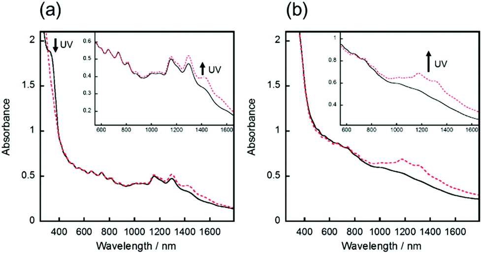 | ||
| Fig. 1 (a) UV-Vis-NIR spectra of the SWCNT/AB hybrids in (a) propylene carbonate solution, and (b) solid film. The black solid and red dashes lines indicate the absorption spectra before and after UV irradiation (365 nm, 20 mW cm−2, and 2 min), respectively. | ||
Based on these results, it appears that the spectral changes are caused by doping and de-doping effects of the photoisomerised AB. Indeed, it has been known that the absorption bands of S11 are bleached by doping with acids (e.g. H2SO4 and HNO3).31–33 In our case, the absorption spectrum of the SWCNT/AB film indicates the bleached S11 bands compared with that of the SWCNT/SDOC film and the SWCNT/AB film with UV irradiation. Collectively, these results showed that the as-prepared SWCNT film was doped by AB, and the appearance of the S11 bands following UV irradiation should correspond the de-doping of photoisomerised AB. The photochemical change of the sheet resistance of the SWCNT/AB film supports this scheme.33 After UV irradiation, the sheet resistance of the SWCNT/AB film increased 3 times (from 3.1 × 10³ to 9.5 × 10³ Ω sq−1), suggesting the de-doping of SWCNT by the structural change of AB on the hybrid (Table S1†). These results indicate that the SWCNT/AB hybrid can output two signals, as evidenced by changes in NIR absorption and conductivity, following the input of one signal (UV light). Notably, almost all previously reported photoactive carbon nanomaterials comprise one-to-one relations between input and output.34,35
Reversible changes of absorbance were observed following the irradiation of visible light or thermal treatment at 100 °C. Following the visible light irradiation (436 nm, 10 mW cm−2) to the UV-irradiated SWCNT/AB film, the gradual decrease of the S11 absorption bands was observed (Fig. 2a). After 20 min of irradiation, the absorption spectra were recovered to that before UV irradiation. This spectral change demonstrated that the doping of the SWCNT by AB occurred again due to the reverse photoreaction of AB from the cis state to trans one.14 Over five cycles of switching between doping and de-doping of AB by alternating UV and visible irradiation, the absorbance change was basically consistent (Fig. 2b). Additionally, the switching of the sheet resistance of the SWCNT/AB film was also observed following the UV and visible light irradiations (Fig. S3†). When the UV-irradiated SWCNT/AB film was held at 100 °C, a decrease of the S11 absorption bands was evident (Fig. 3a). It has been known that azobenzene can interchange between the cis and trans states not only by visible light but also by thermal treatment.23 Clearly, the presence of AB in the hybrid suggests a thermal reverse reaction, and the SWCNT/AB film indeed exhibited a decrease in the S11 absorption bands at high temperature. In contrast, the similar decrease of absorbance was not observed when the UV-irradiated SWCNT/AB film was held at relatively low temperature of 25 °C (Fig. 3b and c). Held at 25 °C for 96 h, the SWCNT/AB film showed only a slight decrease of absorbance (the change of absorbance at 1310 nm was 0.012) due to the suppression of the thermal cis to trans back reaction.
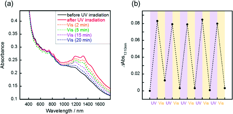 | ||
| Fig. 2 (a) UV-Vis-NIR spectral change of the SWCNT/AB hybrid film with UV (365 nm, 20 mW cm−2, 2 min) and visible light (436 nm, 10 mW cm−2, 20 min) irradiation. (b) Absorbance change ratio at 1310 nm (ΔAbs1310) of the SWCNT/AB hybrid film with UV and visible light irradiation. | ||
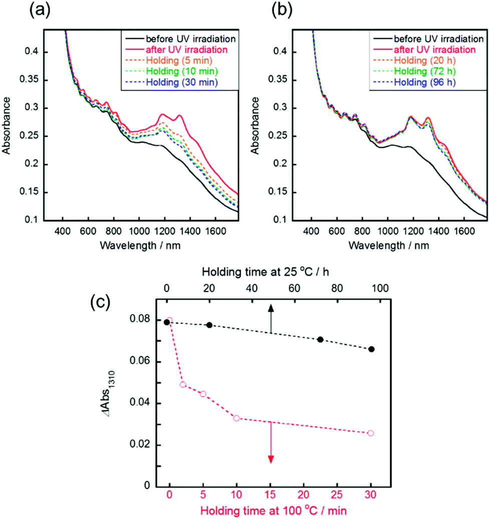 | ||
| Fig. 3 (a) UV-Vis-NIR spectral change of the SWCNT/AB hybrid film with holding at (a) 100 °C and (b) 25 °C. (c) Time-dependent change of ΔAbs1310 at 25 °C (black solid circle) and (b) 25 °C (red open circle). | ||
To clarify the doping effect of AB on SWCNT in the SWCNT/AB solid film, Raman spectroscopy was also performed. Upon UV irradiation, the G band of the SWCNT in the SWCNT/AB film showed a blue-shift (from 1590 cm−1 to 1594 cm−1) with respect to that of the unirradiated film (Fig. 4a). Following visible light irradiation, the G band was red-shifted to the original position (from 1594 cm−1 to 1590 cm−1). As a control, the Raman spectrum of the SWCNT/SDOC film was also recorded. The G band of the SWCNT in this film was always observed at 1590 cm−1 with and without UV irradiation (Fig. 4b). On the basis of these studies, the observed shifts in the G band with UV and visible light for SWCNT/AB can be attributed to the photo-isomerisation of the attached AB.14 Upon UV irradiation, AB converts from the trans form to the cis one leading doping and de-doping, respectively. These conclusions are supported by the I2D/IG ratio, as doping effects are apparent from a decrease of this ratio.36 Table S1† summarises the I2D/IG ratio in several conditions. The I2D/IG of SWCNT/AB is 0.32, which is reduced relative to that of SWCNT/SDOC (0.53), indicating that the SWCNT was doped by AB. Upon UV irradiation, the I2D/IG increased to 0.36, indicating de-doping by the photo-isomerised AB.
 | ||
| Fig. 4 Raman spectra of (a) SWCNT/AB and (b) SWCNT/SDOC films on glass substrate as prepared (black line), with UV irradiation (blue line), and with Vis irradiation (red line). Excitation wavelength is 532 nm. | ||
The surface morphology of the SWCNT/AB film on glass substrate before and after UV irradiation was also examined using AFM (Fig. S4†). No clear differences were observed before or after UV irradiation, indicating that the switching behaviour occurred only as a molecular-scale photoreaction and not as a macroscopic-scale phenomenon.
Schematic images of the light-induced doping and de-doping of AB in the solid film are shown in Fig. 5. It is known that the energy level of SWCNTs are affected by the trans-to-cis transformation of nearly-located azobenzene.14,37 As in our previous work in a liquid condition,23 we observed macroscopic changes of the SWCNT/AB hybrid dispersion from a uniform dispersive state to a precipitative one caused by the detachment of the photo-isomerised AB from the SWCNT surface into a solvent following UV light irradiation (Fig. S5†). Thus, absorption bands of the SWCNT were not observed in the solution state. By comparison, molecular movement is limited in the present solid films, so the SWCNT and AB can interact strongly and the photo-isomerisation cycle of AB is believed to occur on the SWCNT surface. That is the reason why the SWCNT/AB film showed drastic and reversible changes of optical and electrical properties.
 | ||
| Fig. 5 Schematic representation of the light-induced switching of AB (only the cationic part is displayed) on the SWCNT surface in solid film. | ||
It was found that the absorbance of the S11 bands could be controlled not only by irradiation time but also by the intensity of the UV light. We irradiated UV light to the SWCNT/AB film at different intensities and time (Fig. S6a and S6b†). Following irradiation with low intensity UV light (2 mW cm−2), the rate of increase and the change of absorbance were lower than that following irradiation with high intensity light (20 mW cm−2) (Fig. S6c†). When we convert the irradiation time to irradiation energy (mJ cm−2), a similar rate increase of absorbance is observed under different irradiation intensities, indicating that the increase of the rate of absorbance is strongly dependent on the total irradiated energy (Fig. S6d†).
Conclusions
In conclusion, we demonstrated the light-induced switching of both the optical and electrical properties of SWCNTs film by using the photoresponsive dispersant AB. The hybridisation of SWCNT and AB selectively reduces the absorbance of the semiconducting SWCNTs (S11) because of the doping effect of AB. UV irradiation causes the photoisomerisation of AB, thereby reducing its doping ability and thus increasing of the absorbance of S11. These absorbance changes were controllable by changing the intensity of the UV light and the irradiation time, and they were switchable by visible light irradiation and thermal treatment. Further, the hybrid film was fabricated using a simple wet-coating method, which is advantage in terms of cost, controllability of film properties, and can fabricate on various substrates. Overall, this SWCNT hybrid shows great potential for optoelectronic devices, sensors, and optical filters.Conflicts of interest
There are no conflicts to declare.Acknowledgements
This work was supported by the fundamental research fund of AIST. We thank Dr Hideyuki Kihara of AIST for discussions on the photoresponsive dispersant, and Dr Tadatake Sato and Aiko Narazaki of AIST for assistance with the Raman spectroscopic measurements.References
- J. Du, S. Pei, L. Ma and H. M. Cheng, Adv. Mater., 2014, 26, 1958–1991 CrossRef CAS PubMed.
- J. W. Jo, J. W. Jung, J. U. Lee and W. H. Jo, ACS Nano, 2010, 4, 5382–5388 CrossRef CAS PubMed.
- C. Cao, J. B. Andrews, A. Kumar and A. D. Franklin, ACS Nano, 2016, 10, 5221–5229 CrossRef PubMed.
- Y. Yang, L. Ding, J. Han, Z. Zhang and L.-M. Peng, ACS Nano, 2017, 11, 4124–4132 CrossRef CAS PubMed.
- X. He, W. Gao, L. Xie, Q. Zhang, S. Lei, B. Li, J. M. Robinson, S. K. Doorn, R. Vajtai, P. M. Ajayan and W. W. Adams, Nat. Nanotechnol., 2016, 11, 633–640 CrossRef CAS PubMed.
- X. He, N. Fujimura, J. M. Lloyd, K. J. Erickson, A. A. Talin, Q. Zhang, W. Gao, Q. Jiang, Y. Kawano, R. H. Hauge, F. Léonard and J. Kono, Nano Lett., 2014, 14, 3953–3958 CrossRef CAS PubMed.
- T. Fukumaru, T. Fujigaya and N. Nakashima, Macromolecules, 2013, 46, 4034–4040 CrossRef CAS.
- G. W. Huang, H. M. Xiao and S. Y. Fu, J. Mater. Chem. C, 2014, 2, 2758–2764 RSC.
- C. Subramaniam, A. Sekiguchi, T. Yamada, D. N. Futaba and K. Hata, Nanoscale, 2015, 8, 3888–3894 RSC.
- D. Benetti, K. T. Dembele, J. Benavides, H. Zhao, S. Cloutier, I. Concina, A. Vomiero and F. Rosei, J. Mater. Chem. C, 2016, 4, 3555–3562 RSC.
- Q. Wang, S.-F. Lee, C. Tang, J. C.-M. Yu, K. C.-F. Leung and K.-W. Wong, RSC Adv., 2014, 4, 18193–18197 RSC.
- L. Zhou, Q. Liu, X. Lv, L. Gao, S. Fang and H. Yu, J. Mater. Chem. C, 2016, 4, 9993–9997 RSC.
- K. R. Devi, C. L. Lekshmi, K. Joseph and S. Mahesh, ACS Appl. Mater. Interfaces, 2016, 9, 1167–1172 Search PubMed.
- S. Li, Y. Feng, P. Long, C. Qin and W. Feng, J. Mater. Chem. C, 2017, 5, 5068–5075 RSC.
- Y. Wang, H. Mi, Q. Zheng, Z. Ma and S. Gong, ACS Appl. Mater. Interfaces, 2015, 7, 2641–2647 CAS.
- W. Feng, C. Qin, Y. Shen, Y. Li, W. Luo, H. An and Y. Feng, Sci. Rep., 2015, 4, 3777 CrossRef PubMed.
- J. Zhao and J. Ma, J. Phys. Chem. C, 2016, 120, 25131–25141 CAS.
- A. M. Kolpak and J. C. Grossman, Nano Lett., 2011, 11, 3156–3162 CrossRef CAS PubMed.
- A. M. Kolpak and J. C. Grossman, J. Chem. Phys., 2013, 138, 34303 CrossRef PubMed.
- M. Kim, N. S. Safron, C. Huang, M. S. Arnold and P. Gopalan, Nano Lett., 2012, 12, 182–187 CrossRef CAS PubMed.
- A. R. Jang, E. K. Jeon, D. Kang, G. Kim, B. S. Kim, D. J. Kang and H. S. Shin, ACS Nano, 2012, 6, 9207–9213 CrossRef CAS PubMed.
- Y. Matsuzawa, Y. Takada, T. Kodaira, H. Kihara, H. Kataura and M. Yoshida, J. Phys. Chem. C, 2014, 118, 5013–5019 CAS.
- H. Jintoku, Y. Matsuzawa, H. Kihara and M. Yoshida, Chem. Lett., 2016, 45, 1307–1309 CrossRef CAS.
- H. Jintoku, T. Sato, T. Nakazumi, Y. Matsuzawa, H. Kihara and M. Yoshida, ACS Appl. Mater. Interfaces, 2017, 9, 30805–30811 CAS.
- Y. Matsuzawa, H. Kato, H. Ohyama, D. Nishide, H. Kataura and M. Yoshida, Adv. Mater., 2011, 23, 3922–3925 CrossRef CAS PubMed.
- O. V. Kharissova, B. I. Kharisov and E. G. de Casas Ortiz, RSC Adv., 2013, 3, 24812 RSC.
- T. Fujigaya and N. Nakashima, Sci. Technol. Adv. Mater., 2015, 16, 24802 CrossRef PubMed.
- K. Mulla, S. Liang, H. Shaik, E. a. Younes, A. Adronov and Y. Zhao, Chem. Commun., 2015, 51, 149–152 RSC.
- M. J. O'Connell, S. M. Bachilo, C. B. Huffman, K. L. Rialon, P. J. Boul and W. H. Noon, Science, 2002, 297, 593–597 CrossRef PubMed.
- Y. Kato, A. Inoue, Y. Niidome and N. Nakashima, Sci. Rep., 2012, 2, 733 CrossRef PubMed.
- Y. Nonoguchi, K. Ohashi, R. Kanazawa, K. Ashiba, K. Hata, T. Nakagawa, C. Adachi, T. Tanase and T. Kawai, Sci. Rep., 2013, 3, 3344 CrossRef PubMed.
- H. Wang, P. Wei, Y. Li, J. Han, H. R. Lee, B. D. Naab, N. Liu, C. Wang, E. Adijanto, B. C.-K. Tee, S. Morishita, Q. Li, Y. Gao, Y. Cui and Z. Bao, Proc. Natl. Acad. Sci., 2014, 111, 4776–4781 CrossRef CAS PubMed.
- J. L. Blackburn, T. M. Barnes, M. C. Beard, Y. Kim, C. Robert, T. J. Mcdonald, B. To, T. Coutts and M. J. Heben, Renewable Energy, 2008, 2, 1266–1274 CAS.
- W. Feng, W. Luo and Y. Feng, Nanoscale, 2012, 4, 6118–6134 RSC.
- X. Zhang, L. Hou and P. Samorì, Nat. Commun., 2016, 7, 11118 CrossRef CAS PubMed.
- A. C. Ferrari and D. M. Basko, Nat. Nanotechnol., 2013, 8, 235–246 CrossRef CAS PubMed.
- J. M. Simmons, I. In, V. E. Campbell, T. J. Mark, F. Léonard, P. Gopalan and M. A. Eriksson, Phys. Rev. Lett., 2007, 98, 86802 CrossRef CAS PubMed.
Footnote |
| † Electronic supplementary information (ESI) available: UV-Vis-NIR spectra, and AFM images. See DOI: 10.1039/c8ra01447g |
| This journal is © The Royal Society of Chemistry 2018 |