DOI:
10.1039/C8RA01382A
(Paper)
RSC Adv., 2018,
8, 21040-21046
Optical constants acquisition and phase change properties of Ge2Sb2Te5 thin films based on spectroscopy
Received
13th February 2018
, Accepted 1st June 2018
First published on 8th June 2018
Abstract
In this work, phase change chalcogenide Ge2Sb2Te5 (GST) thin films were fabricated by magnetron sputtering. The optical properties, especially the optical constants (refractive index and extinction coefficient), of such alloys were systematically studied by investigating their thermally and photo-thermally induced switching between different phases. The results show that GST films are highly tunable in microstructure and optical constants, either by post-annealing at 160 °C, 200 °C, 250 °C and 350 °C, respectively, or by laser irradiation of 1 mW, 3 mW, 5 mW and 10 mW power with beam diameter of 7 μm at 532 nm, respectively. From the structural analysis, we can clearly observe different crystallinities and chemical bonding in the different post-treated GST films. The optical constants of GST films under various phases were obtained from spectrophotometry, by fitting their transmittance data with the Tauc–Lorentz (TL) dispersion model. The refractive index and extinction coefficient exhibit notable change upon annealing and laser irradiation, specifically at 1550 nm, from 3.85 (amorphous) to 6.5 (crystalline) in refractive index. The optical constants have been proved capable of fine tuning via the laser irradiation method. Hence, the pronounced adjustability in optical properties due to rapid and repeatable phase change render GST suitable for tunable photonic devices.
Introduction
Chalcogenide glasses (ChGs), a notable branch of amorphous semiconductors, have been widely applied as critical materials in phase-change memories, sensors and photonic devices.1 One of the most attractive properties of ChGs is their outstanding phase changing characteristic, making them suitable candidates for building rewritable storage devices, multi-color tunable filters, and electrically- or optically- driven intelligent displays.2–6 In addition, the high material nonlinearity of GST, combined with the strong confinement and dispersion in fiber and waveguide devices, makes it attractive for fast nonlinear optical devices.7,8 However, there are also some deficiencies in the performance of GST, especially its relatively large optical nonlinear absorption in the optical communication band and poor chemical and thermal stability.9,10
Nowadays, phase change materials (PCMs) are the focus of scientific research.11–13 Ge-Sb-Te (GST) is a relatively mature and superior PCM which can be classified into three categories: Ge1Sb2Te4, Ge1Sb4Te7 and Ge2Sb2Te5. Most researchers are interested in Ge2Sb2Te5 due to its faster crystallization rate, lower power consumption, as well as the undemanding composition requirements that minor composition deviation does not affect the performance.14–16 Our research focuses on tracking the GST optical constant evolution process during the successive stages of phase-change. As there are coexistence of different proportion of amorphous and crystalline phases at different phase transformation stages. The optical constants obtained from various stages are proved to be continuously variable. It is therefore possible to realize the precise modulation on optical properties of GST chalcogenide by tracking their optical constants at different phase stages. It is also helpful for data support to the phase transformation physics.
In this paper, Ge2Sb2Te5 films with controllable composition and tunable optical properties were successfully fabricated. For the determination of optical constants, the transmittance data in the NIR region were fitted with Tauc–Lorentz model and thus, the refractive index and extinction coefficient were effectively retrieved. Hence, the correspondence of post treatment process and optical constants of GST films make it possible to fine control optical properties of chalcogenide materials in NIR range. On this basis, the utilization of GST films in designing and manufacturing a variety of photonic integrated devices in the field of optical communication, interconnection and computing will be realized. It is worth mentioning that GST films have large absorption in the visible region resulting in a very low transmittance (almost near zero). Thus, compared with spectroscopic ellipsometry, the method based on transmittance spectra are relatively inaccurate to obtain optical constants in visible region. This paper focuses on the optical constants acquisition in the near-infrared band.
Experimental and theoretical basis
Fabrication
The Ge2Sb2Te5 thin films were fabricated with magnetron sputtering method. A Ge2Sb2Te5 ceramic target with diameter of 3 inch was located 15 cm away from the rotatable sample stage. 150 nm-thick Ge2Sb2Te5 composite films were deposited on BK7 glass substrates. The radiofrequency (RF) sputtering power was fixed at 80 W and the substrates temperature was set at room temperature (RT). Some as-deposited samples were annealed in vacuum atmosphere for 20 minutes under four temperatures: 160 °C, 200 °C, 250 °C and 350 °C, respectively. Some others were irradiated by 532 nm continuous wave (CW) laser (diameter size of the laser spot is 7 μm) with beam power of 1 mW, 3 mW, 5 mW and 10 mW, respectively.
Characterization
The composition of as-prepared Ge2Sb2Te5 thin films determined by energy dispersive spectrometer (EDS, X-Max 20) was 22.00 at% Ge, 24.75 at% Sb, and 53.25 at% Te, which is very close to a nominal composition of bulk GST material (Ge22.2Sb22.2Te55.6). The film thickness was in situ controlled by quartz crystal monitor. Transmission electron microscopy (TEM, Tecnai G2) and Raman spectroscopy (Horiba Jobin Yvon, LabRAM HR Evolution) were applied to analyze the microstructures of GST films. The crystallinity of each sample was retrieved from X-ray diffractometer (XRD, Panalytical B.V. X-pert Powder). Spectrophotometer (Agilent Cary-7000) was used to obtain the transmittance for GST films on glasses.
Optical constant acquisition
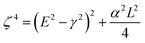
The dispersion behavior of narrow gap semiconductor chalcogenide films can be well described by the classic Tauc–Lorentz model.17,18 This oscillation function (eqn (1)) describes the complex dielectric permittivity as:17,19| |
 | (1) |
| |
 | (2) |
where  and
and  are the real part and imaging part of complex permittvity, respectively. A is the amplitude (oscillator strength), L is the broadening term, Eg is the optical bandgap energy and E0 is the peak transition energy. The eqn (2) is workable when photon energy E > Eg, otherwise
  is 0.
is 0.
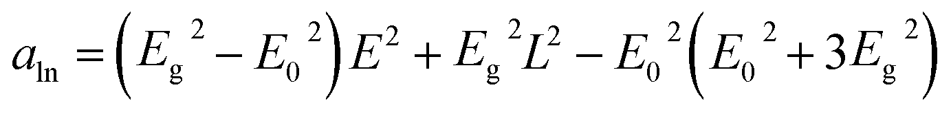
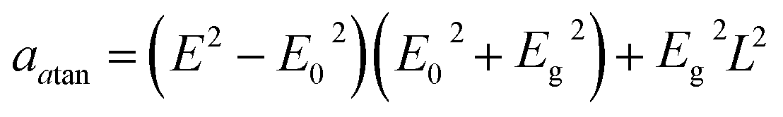
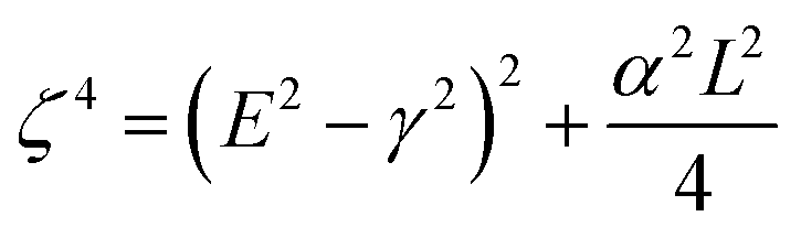
The real part of the permittvity  can be obtained by Kramers–Kronig integration, which can be solved in closed form, and is given by20
| |
 | (3) |
where
| |
 | (4a) |
| |
 | (4b) |
| |
 | (4c) |
| |
 | (4d) |
| |
 | (4e) |
For the sake of convenience, eqn (2) and (3) are marked as f2 and f3 respectively. Refractive index (n) and extinction coefficient (k) can therefore be given by
| |
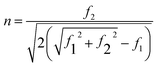 | (5) |
| |
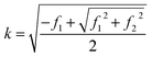 | (6) |
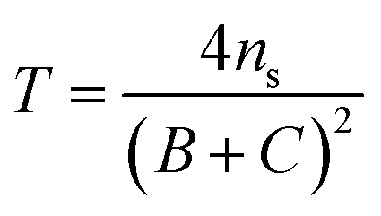
According to the characteristic matrix formalism of the thin film available, equation of transmittance is given by21,22
| |
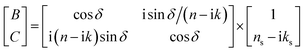 | (7) |
| |
 | (8) |
where
δ = 2π
d(
n − i
k)/
λ is the phase angle of the film,

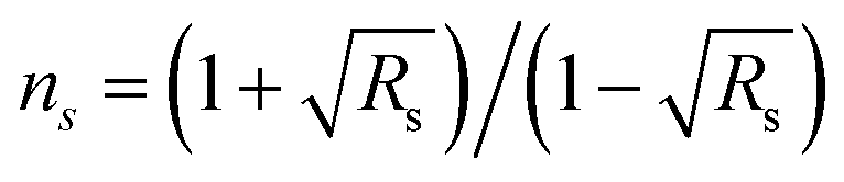
is the refractive index of substrate,
Rs = 1 −
Ts is the reflectivity index of substrate (in the wavelength range between 700–2000 nm, the extinction coefficient of BK7 glass is approximately zero),
Ts is the transmittance of substrate and
d is the physical thickness of film.
Combining the above formulas, we can establish the relationship between film transmittance T and wavelength λ. On the basis of the transmittance data we measured, MATLAB software was used to fit the transmittance curve so that six parameters in above equations (A, L, Eg, E0,  (∞) and d) could be obtained. Substituting these parameters into eqn (5) and (6), wavelength dependence of refraction index (n) and extinction coefficient (k) were therefore retrieved. The fitting algorithm used in the above process was the simplex, which can be replaced by other effective optimizing algorithms.
Results and discussions
XRD and Raman analysis
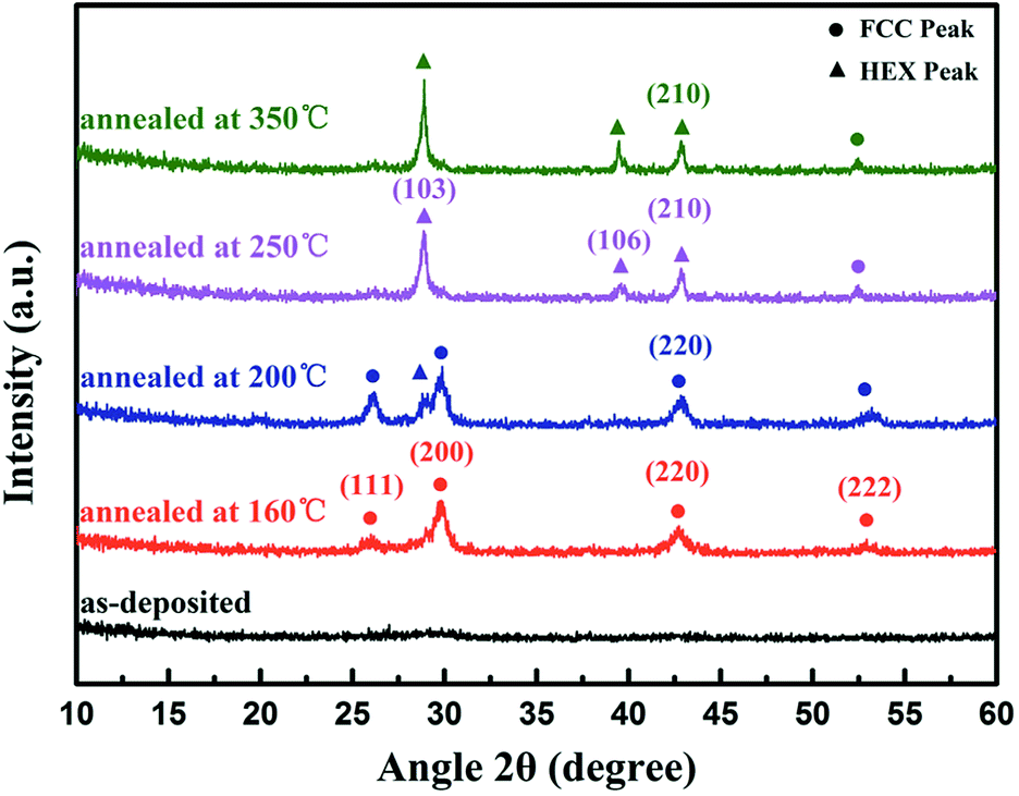
In order to investigate and verify the phase change process of GST films, we utilized XRD measurements for the as-deposited and annealed GST films. As shown in Fig. 1, the films deposited at RT have no obvious crystal diffraction peaks, indicating that the films are primarily amorphous. With the increase of annealing temperature, the XRD patterns exhibit the following two-stage changes: at stage one (160–200 °C), the diffraction peak appears at two theta of 26.2° (111), 29.8° (200), 42.6° (220) and 58.1° (222),23,24 corresponding to face-centered cubic (FCC) phase structure (marked with black solid dot). At stage two (above 200 °C), new diffraction peaks (marked with black solid triangle) appears at 28.6° (103), 39.8° (106) and 43.1° (210),25,26 and their intensity increase as the annealing temperature increases. However, the (111) and (220) peaks from FCC were found gradually disappeared, indicating that GST films are transformed into HEX-phase structure.
 |
| | Fig. 1 X-ray diffraction patterns of GST films in θ–2θ mode at different temperatures. | |
Fig. 2 shows the Raman scattering spectra of GST films. Our measurements show that for the as-deposited films, a broad envelop peak around 145 cm−1 was the main feature in the curve, it is assigned to the Sb–Te vibrations in SbTe3 pyramidal units, or may from defective octahedral coordination of Sb atoms.27–29 In addition, another broad Raman band peaking at ∼125 cm−1 and a weak band peaking at ∼220 cm−1 of amorphous GST films can be attributed to the A1 mode of GeTe4−nGen (n = 1, 2) corner-sharing tetrahedra and F2 mode of GeTe4 tetrahedra, respectively.30–32 For the 160 °C and 200 °C annealed GST films, the Raman band at ∼145 cm−1 is gradually weakened and the band at ∼125 cm−1 (for amorphous GST films) is decomposed into ∼105 cm−1 and ∼135 cm−1 vibration modes for crystalline phase (FCC configuration). The first one (∼105 cm−1) could be attributed to the softened A1 mode of corner-sharing GeTe4 tetrahedra, and the latter (∼135 cm−1) one to the A1 mode of corner-sharing GeTe4−nGen (n = 1, 2) tetrahedra.32 For the samples annealed at higher temperatures (above 200 °C), the Raman band peaking at ∼145 cm−1 is disappeared and new bands at ∼110 cm−1 and ∼165 cm−1 are formed (for both FCC and HEX crystallized GST films), which are assigned to vibrations of GeTe Γ1(A1) Eg(2) and A1g(2) modes of hexagonal Sb2Te3.32–34 It is worth mentioning that, since the GST Raman spectrum is displayed as broad envelope curves at different GST phase stages implying multiple peaks overlapping, it is not easy to identify each peak accurately. We therefore tried to use Gaussian distributions of several vibration peaks to segment and fit the envelope curves of the 200 °C annealed sample. The distinguishable peaks (A, B, C, D, E and F) was shown in the inset of Fig. 2, which shows a representative fitting result of this Raman spectrum.
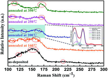 |
| | Fig. 2 Raman spectra of Ge2Sb2Te5 films annealed at temperatures from room temperature to 350 °C. Inset: representative fitting result of the Raman spectrum of sample annealed at 200 °C with six Gaussian distributions (A, B, C, D, E and F). For the sake of splitting, the original Raman curve is smoothed. | |
The Raman spectra evolution during post-annealing process is believed to be caused by microstructure changes of GST film from the amorphous state to FCC, then to HEX structure as the annealing temperature increases, since the atomic arrangements and network environments in the above phases are different.35
Microstructure analysis
In order to depict the microstructural evolution of GST films at various phases, high-resolution TEM was used to obtain the cross section images and selected-area electron diffraction patterns. Fig. 3 shows the results for as-deposited (Fig. 3(a) and (b)), 200 °C annealed (Fig. 3(c) and (d)) and 350 °C annealed ((Fig. 3(e) and(f))) GST films (representing amorphous, face-centered cubic phase and hexagonal phase), respectively. From Fig. 3(a), GST films deposited at room temperature was shown as typical amorphous phase. No distinct diffraction spots are observed overlaying on dispersive haloes (Fig. 3(b)). When the samples were annealed at 200 °C, diffraction fringes indicating various orientational crystalline lattices can be observed (Fig. 3(c) and (d)), implying the formation of nano FCC particles. When the annealing temperature was risen to 350 °C, GST films show increased crystallinity as clearer fringes, exhibiting hexagonal (HEX) phase polycrystalline structure (Fig. 3(e)). In Fig. 3(f) superimposed diffraction spots also reveal that the formation of HEX phase crystal lattices.
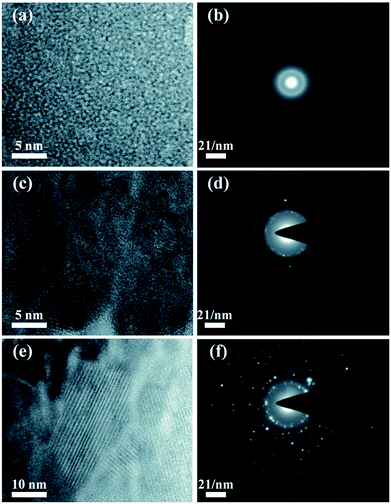 |
| | Fig. 3 TEM images and the selected-area diffraction patterns of Ge2Sb2Te5 films in different phases: (a) and (b) as-deposited, (c) and (d) annealed at 200 °C, (e) and (f) annealed at 350 °C. | |
Analysis of optical properties during thermally-induced phase change
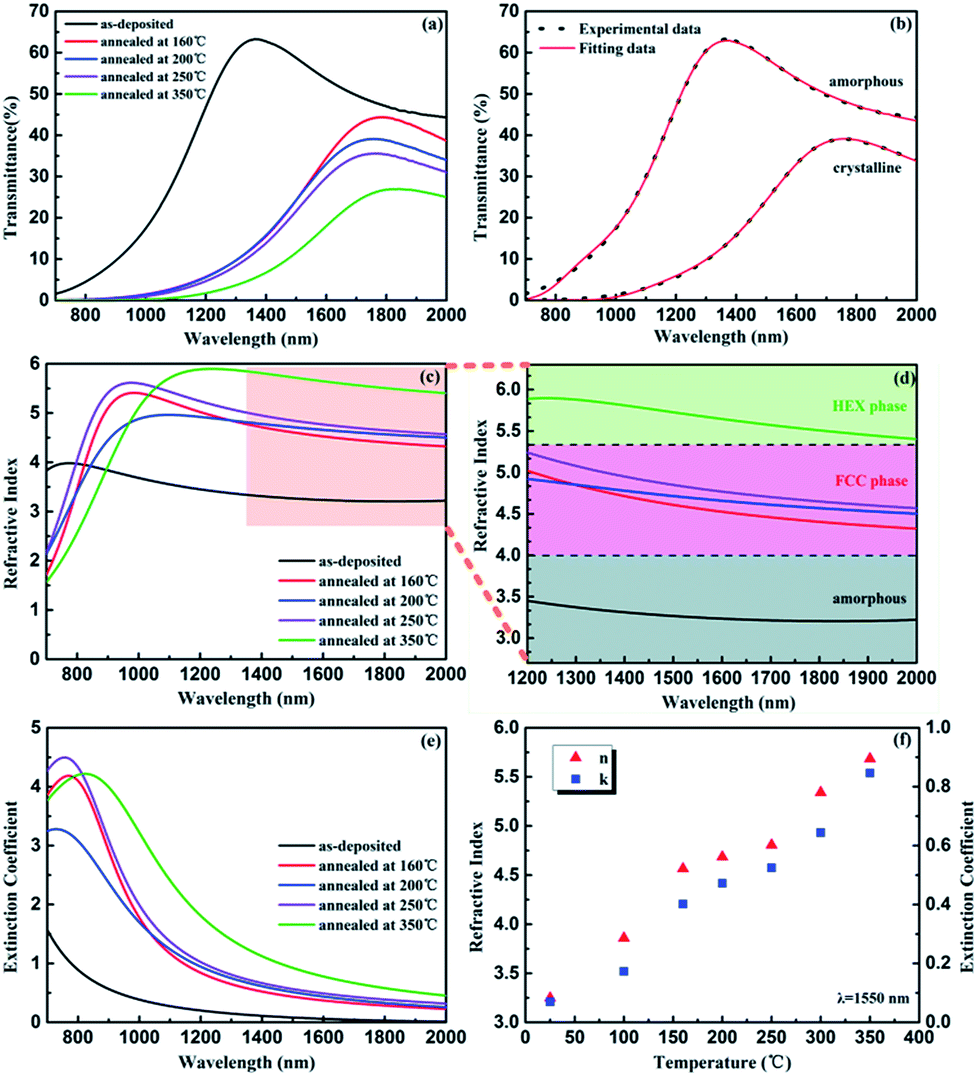
We measured the transmittance of GST films in the range of 700 nm and 2000 nm by the spectrometer (Fig. 4(a)). The transmittance curves are monotonically decrease as the annealing temperature increases. In order to further study the optical properties before and after the GST phase changing, we retrieved optical constants by optimizing each transmittance curve to fit the measured results according to suitable dispersion model. The fitting schematic for amorphous and crystalline GST (a-GST and c-GST) films are shown in Fig. 4(b). The fitting data are found perfectly coincide with the transmittance curves by using TL dispersion model. Thus we are able to obtain reasonable and reliable optical constants (i.e. refractive index n and extinction coefficient k) of GST thin films at different phase stage. In Fig. 4(c) and (e), n and k for GST films in different phases are plotted and manifest great changes during the phase changing process. Fig. 4(d) is the enlarged view of Fig. 4(c) at the wavelength region from 1200 nm to 2000 nm, and the curves for n can be clearly distinguished in three index areas, coinciding with three different phases (amorphous, FCC and HEX) identified from the XRD measurement. On the other hand, the extinction coefficient k also increases which means larger optical loss after annealing. Considering the optical communication wavelength 1550 nm as an example, as depicted in Fig. 4(f), the refractive index n can reach around 5.7 after phase transformation, and the extinction coefficient is acceptable (less than 0.9). Therefore, we can utilize the giant change of refractive index of GST at communication wavelength in the applications of information storage and optical modulation.
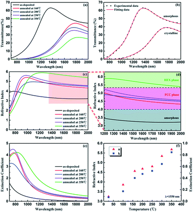 |
| | Fig. 4 (a) Measured transmissivity (T) curves of Ge2Sb2Te5 films at different temperatures, (b) experimental measured datas by spectrometer and fitting results by TL dispersion model for as-deposited a-GST and 200 °C annealed c-GST, (c) and (d) refractive index (n) results of GST at different temperatures and the enlarged view at 1200–2000 nm, (e) extinction coefficient (k) results of GST at different temperatures, (f) refractive index (n) and extinction coefficient (k) results of GST at different temperatures in 1550 nm wavelength. | |
Analysis of laser-induced phase change
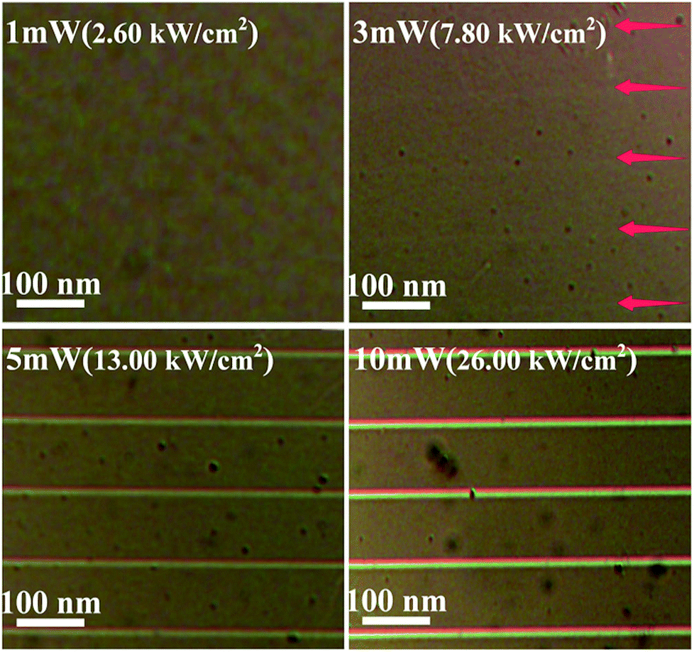
Owing to the shortage in patterning of optical constants modulation, as well as the time-consuming of thermal induced phase transition, we further explore the photo-thermal induced phase transition method by using focused CW laser beam at 532 nm. As shown in Fig. 5, the as-deposited GST films were irradiated by laser with different power (1 mW, 3 mW, 5 mW and 10 mW, respectively). The power densities of laser beam were 2.60 kW cm−2, 7.80 kW cm−2, 12.99 kW cm−2 and 25.98 kW cm−2 under 7 μm diameters beam spot. The CW laser beam irradiated the film surface in a scanning mode, with the horizontal scanning rate of 5.8 μm s−1 and the vertical scanning step of 100 μm. The scanning area of each GST film was set as 2 mm × 2 mm. The reflectance optical microscopy images in Fig. 5 shows a series of transverse bright stripes with different brightness. The bright streaks were the traces of laser irradiation, which occupied a certain percentage of the scanning area. And the percentage can be tuned by setting different vertical scanning steps of laser beams so that the surface morphology and the transmittance of entire area could be carefully adjusted. On the basis of the results in Fig. 5, the film surface microstructure almost has not changed when power was under some threshold (1 mW, 2.60 kW cm−2). As laser power density increases, the brightness of stripes on film surface became more and more intensified after irradiation, especially at 10 mW laser power (25.98 kW cm−2).
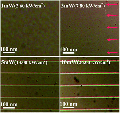 |
| | Fig. 5 The reflectance optical microscopy images of Ge2Sb2Te5 film surfaces irradiated by laser at 1 mW (2.60 kW cm−2), 3 mW (7.80 kW cm−2), 5 mW (12.99 kW cm−2) and 10 mW (25.98 kW cm−2) power respectively. | |
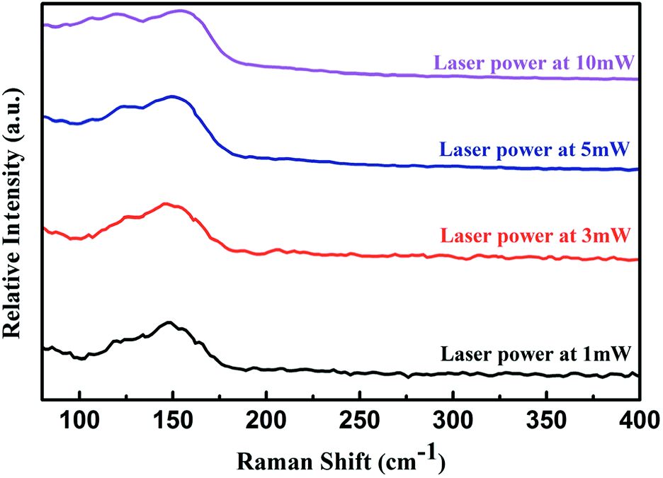
Fig. 6 shows the Raman spectra of laser-induced GST films by different beam power. In order to reduce the impact of Raman laser source, GST films was measured under 1 mW power of Raman laser. In the spectra, a broad peak appeared around 150 cm−1. As the laser power increases, the initial peak is gradually divided into two seperated peaks at 110 cm−1 and 165 cm−1, which means different degrees of phase change occurred in GST films under different laser powers.
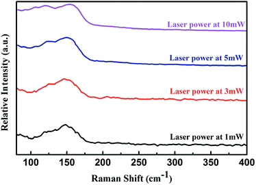 |
| | Fig. 6 Raman spectra of Ge2Sb2Te5 films irradiated at different laser powers from 1 mW to 10 mW by 1 mW Raman laser. | |
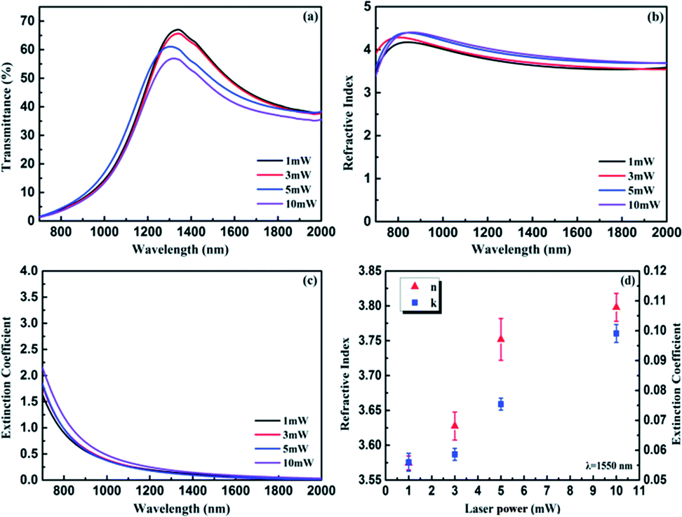
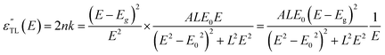
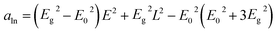
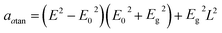
In order to figure out the trend of optical constants evolution of GST films after irradiated by different laser powers. The dispersion curves of refractive index (n) and extinction coefficient (k) were obtained by using TL dispersion model (see in Fig. 7(b) and (c)). Since the laser irradiated only a part of the surface of GST films in the region of 2 mm × 2 mm area, which can be seen from Fig. 5 that the irradiated area accounts for a small proportion of the entire area, the transmittance that reflected in the result of Fig. 7(a) changed slightly. The variation of refractive index and extinction coefficient from Fig. 7(b) and (c) shows that laser can indeed induce GST films to phase change and transform the optical constants by different laser powers. Fig. 7(d) shows that refractive index (from 3.57 to 3.80) and extinction coefficient (from 0.055 to 0.099) are tuned subtly at 1550 nm wavelength as laser power increased. In addition, optical constants of GST films can be easily controlled through changing the portion of the laser irradiation area. Herein some important fitting parameters and optical constants at 1550 nm of GST films treated by thermal annealing and laser irradiation are shown in Table 1.
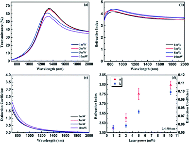 |
| | Fig. 7 (a) Measured transmissivity (T) curves of laser-induced Ge2Sb2Te5 films at different laser powers, (b) refractive index (n) and (c) extinction coefficient (k) results of GST induced by different laser powers, (d) refractive index (n) and extinction coefficient (k) error bars of GST with different laser powers at 1550 nm wavelength. | |
Table 1 Fitting Tauc–Lorentz model parameters of the studied GST thin films at as-deposited state, different annealling temperatures and laser irradiation powers. A, Eg, E0 and d are Lorentz oscillator amplitude, optical band energy, resonance energy and film thickness. n and k represent refractive index and extinction coefficient at 1550 nm, respectively
| |
As-deposited |
Annealed at 160 °C |
Annealed at 200 °C |
Annealed at 250 °C |
Annealed at 350 °C |
Laser power at 1 mW |
Laser power at 3 mW |
Laser power at 5 mW |
Laser power at 10 mW |
| A (eV) |
109.4 ± 0.5 |
110.7 ± 0.6 |
183.4 ± 0.5 |
189.2 ± 0.5 |
188.5 ± 0.7 |
101.0 ± 0.4 |
106.6 ± 0.4 |
105.6 ± 0.6 |
103.9 ± 0.5 |
| Eg (eV) |
0.652 ± 0.008 |
0.642 ± 0.007 |
0.508 ± 0.008 |
0.46 ± 0.009 |
0.36 ± 0.008 |
0.631 ± 0.006 |
0.635 ± 0.007 |
0.591 ± 0.007 |
0.457 ± 0.008 |
| E0 (eV) |
3.76 ± 0.02 |
1.11 ± 0.02 |
1.72 ± 0.01 |
1.52 ± 0.03 |
1.35 ± 0.03 |
2.765 ± 0.01 |
2.807 ± 0.01 |
2.596 ± 0.02 |
1.995 ± 0.02 |
| d (nm) |
149.2 ± 0.5 |
150.3 ± 0.3 |
148.5 ± 0.3 |
151.4 ± 0.3 |
153.6 ± 0.2 |
150.5 ± 0.4 |
149.1 ± 0.6 |
150.7 ± 0.3 |
147.9 ± 0.3 |
| n |
3.25 ± 0.02 |
4.57 ± 0.02 |
4.69 ± 0.03 |
4.81 ± 0.02 |
5.68 ± 0.02 |
3.57 ± 0.01 |
3.63 ± 0.02 |
3.75 ± 0.03 |
3.79 ± 0.02 |
| k |
0.070 ± 0.003 |
0.402 ± 0.002 |
0.472 ± 0.003 |
0.525 ± 0.04 |
0.847 ± 0.02 |
0.055 ± 0.003 |
0.059 ± 0.002 |
0.075 ± 0.002 |
0.099 ± 0.002 |
Conclusions
In conclusion, GST films can be controllable phase changed by heat annealling and laser irradiation methods. Different annealing temperatures and laser powers will change the internal chemical bonds configurations among atoms, which make the films undergo different phase change (from amorphous to FCC state and then to HEX state). The optical constants (n, k) at different phase states could be obtained by the TL dispersion model. The result shows the refractive index and extinction coefficient of GST films changed significantly from amorphous to crystalline. Compared with thermal-induced phase change process, photo-induced phase change is more convenient and the optical constants of films can be adjusted finely. Such variability of the GST properties could be used to enable new controllable all-optical modulator or absorber devices.
Conflicts of interest
There are no conflicts to declare.
Acknowledgements
This research was supported by the Natural Science Foundation of China (No. 61575176), the National Basic Research Program of China (973 Program, No. 2013CB632104), and the Research Foundation of State Key Laboratory of Modern Optical Instrumentation (MOI 201701).
References
- B. J. Eggleton, B. Luther-Davies and K. Richardson, Nat. Photonics, 2011, 5, 141–148 CrossRef.
- S. G. C. Carrillo, G. R. Nash, H. Hayat, M. J. Cryan, M. Klemm, H. Bhaskaran and C. D. Wright, Opt. Express, 2016, 24, 13563–13573 CrossRef PubMed.
- L. Fan, J. Wang, L. T. Varghese, H. Shen, B. Niu, Y. Xuan, A. M. Weiner and M. Qi, Science, 2012, 335, 447–450 CrossRef PubMed.
- R. Alaee, M. Albooyeh, S. Tretyakov and C. Rockstuhl, Opt. Lett., 2016, 41, 4099–4102 CrossRef PubMed.
- L. Li, H. Lin, S. Qiao, Y. Zou, S. Danto, K. Richardson, J. D. Musgraves, N. Lu and J. Hu, Nat. Photonics, 2014, 8, 643–649 CrossRef.
- B. Gholipour, J. Zhang, K. F. MacDonald, D. W. Hewak and N. I. Zheludev, Adv. Mater., 2013, 25, 3050–3054 CrossRef PubMed.
- M. R. E. Lamont, B. Luther-Davies, D. Y. Choi, S. Madden and B. J. Eggleton, Opt. Express, 2008, 16, 14938–14944 CrossRef PubMed.
- T. D. Vo, H. Hu, M. Galili, E. Palushani, J. Xu, L. K. Oxenløwe, S. J. Madden, D.-Y. Choi, D. A. P. Bulla, M. D. Pelusi, J. Schröder, B. Luther-Davies and B. J. Eggleton, Opt. Express, 2010, 18, 17252–17261 CrossRef PubMed.
- W. Nie, Adv. Mater., 1993, 5, 520–545 CrossRef.
- S. Liu, J. Wei and F. Gan, J. Appl. Phys., 2011, 110, 033503 CrossRef.
- P. Němec, J. Přikryl, V. Nazabal and M. Frumar, J. Appl. Phys., 2011, 109, 073520 CrossRef.
- J. W. Park, S. H. Eom, H. Lee, J. L. F. D. Silva, Y. S. Kang, T. Y. Lee and Y. H. Khang, Phys. Rev. B: Condens. Matter Mater. Phys., 2009, 80, 115209 CrossRef.
- B. S. Lee, J. R. Abelson, S. G. Bishop, D. H. Kang, B. K. Cheong and K. B. Kim, J. Appl. Phys., 2005, 97, 093509 CrossRef.
- P. Li, X. Yang, T. W. W. Maß, J. Hanss, M. Lewin, A.-Y. U. Michel, M. Wuttig and T. Taubner, Nat. Mater., 2016, 15, 870–875 CrossRef PubMed.
- M. Wuttig and N. Yamada, Nat. Mater., 2007, 6, 824–832 CrossRef PubMed.
- K. Du, Q. Li, Y. Lyu, J. Ding, Y. Lu, Z. Cheng and M. Qiu, Light: Sci. Appl., 2017, 6, e16194 CrossRef.
- J. Orava, T. Wágner, J. Šik, J. Přikryl, M. Frumar and L. Beneš, J. Appl. Phys., 2008, 104, 043523 CrossRef.
- H. G. Tompkins and E. A. Irene, Handbook of Ellipsometry, William Andrew Publishing, Norwich NY, 2005 Search PubMed.
- A. S. Ferlauto, G. M. Ferreira, J. M. Pearce, C. R. Wronski, R. W. Collins, X. Deng and G. Ganguly, J. Appl. Phys., 2002, 92, 2424–2436 CrossRef.
- G. E. Jellison and F. A. Modine, Appl. Phys. Lett., 1996, 69, 371–373 CrossRef.
- D. X. Zhu, W. D. Shen and H. Y. Zhen, J. Appl. Phys., 2009, 106, 084504 CrossRef.
- Y. Yin, H. Ye, C. Zhang, W. D. Shen and X. Liu, J. Appl. Phys., 2009, 106, 074103 CrossRef.
- S. Y. Ie, B. T. Bea, Y. Ahn, M. Y. Chang, D. G. You, M. H. Cho, K. Jeong, J.-H. Oh, G.-H. Koh and H. Jeong, Appl. Phys. Lett., 2007, 90, 251917 CrossRef.
- I. H. Park, J. W. Lee and C. W. Chung, Integr. Ferroelectr., 2006, 80, 207–218 CrossRef.
- F. Yan, T. J. Zhu, X. B. Zhao and S. R. Dong, Appl. Phys. A, 2007, 88, 425–428 CrossRef.
- F. Yang, L. Xu, R. Zhang, L. Geng, L. Tong, J. Xu, W. Su, Y. Yu, Z. Ma and K. Chen, Appl. Surf. Sci., 2012, 258, 9751–9755 CrossRef.
- J. Tominaga and N. Atoda, Jpn. J. Appl. Phys., 1999, 38(Part2), L322 Search PubMed.
- O. Uemura, N. Hayasaka, S. Tokairin and T. Usuki, J. Non-Cryst. Solids, 1996, 205, 189–193 CrossRef.
- I. P. Kotsalas, D. Papadimitriou, C. Raptis, M. Vlcek and M. Frumar, J. Non-Cryst. Solids, 1998, 226, 85–91 CrossRef.
- K. S. Andrikopoulos, S. N. Yannopoulos, A. V. Kolobov, P. Fons and J. Tominaga, J. Phys. Chem. Solids, 2007, 68, 1074–1078 CrossRef.
- K. Tsunetomo, T. Sugishima, T. Imura and Y. Osaka, J. Non-Cryst. Solids, 1987, 95, 509–516 CrossRef.
- P. Němec, V. Nazabal, A. Moreac, J. Gutwirth, L. Beneš and M. Frumar, Mater. Chem. Phys., 2012, 136, 935–941 CrossRef.
- I. Watanabe, S. Noguchi and T. Shimizu, J. Non-Cryst. Solids, 1983, 58, 35–40 CrossRef.
- J. S. Lannin, Phys. Rev. B: Solid State, 1977, 15, 3863 CrossRef.
- B. Liu, Z. T. Song, T. Zhang, S. L. Feng and B. M. Chen, Chin. Phys., 2004, 13, 1947 CrossRef.
|
| This journal is © The Royal Society of Chemistry 2018 |
Click here to see how this site uses Cookies. View our privacy policy here. 
 Open Access Article
 This Open Access Article is licensed under a Creative Commons Attribution-Non Commercial 3.0 Unported Licence
 *
*
 and
and  are the real part and imaging part of complex permittvity, respectively. A is the amplitude (oscillator strength), L is the broadening term, Eg is the optical bandgap energy and E0 is the peak transition energy. The eqn (2) is workable when photon energy E > Eg, otherwise
  is 0.
is 0.
 can be obtained by Kramers–Kronig integration, which can be solved in closed form, and is given by20


 is the refractive index of substrate, Rs = 1 − Ts is the reflectivity index of substrate (in the wavelength range between 700–2000 nm, the extinction coefficient of BK7 glass is approximately zero), Ts is the transmittance of substrate and d is the physical thickness of film.
 (∞) and d) could be obtained. Substituting these parameters into eqn (5) and (6), wavelength dependence of refraction index (n) and extinction coefficient (k) were therefore retrieved. The fitting algorithm used in the above process was the simplex, which can be replaced by other effective optimizing algorithms.