
 Open Access Article
 This Open Access Article is licensed under a Creative Commons Attribution-Non Commercial 3.0 Unported Licence
Investigation on the structural, morphological, electronic and photovoltaic properties of a perovskite thin film by introducing lithium halide†
Zhenhua Lin‡
a,
Hai Zhu‡b,
Long Zhoua,
Jianhui Dua,
Chunfu Zhang a,
Qing-Hua Xub,
Jingjing Chang*a,
Jianyong Ouyangc and
Yue Haoa
a,
Qing-Hua Xub,
Jingjing Chang*a,
Jianyong Ouyangc and
Yue Haoa
aState Key Laboratory of Wide Band Gap Semiconductor Technology, Shaanxi Joint Key Laboratory of Graphene, School of Microelectronics, Xidian University, 2 South Taibai Road, Xi'an, China 710071. E-mail: jjingchang@xidian.edu.cn
bDepartment of Chemistry, National University of Singapore, 3 Science Drive 3, Singapore 117543
cDepartment of Materials Science and Engineering, National University of Singapore, 7 Engineering Drive 1, Singapore 117574
First published on 22nd March 2018
Abstract
The performance of perovskite solar cells (PSCs) including device efficiency and stability is mainly dependent on the perovskite film properties which are critically related to the organic cations used. Herein, we studied the role that the inorganic lithium (Li) cation played in perovskite thin films and its influence on crystal growth, film properties, and device performance. We found that within the threshold limit of a 1.0% molar ratio, the Li dopant had a positive effect on the film formation and properties. However, after replacing more MA+ with Li+, the device performance was degraded significantly with reduced short-circuit current density (Jsc) and fill factor (FF) values. With a doping ratio of 10 mol%, the film morphology, crystallinity, photophysical, and electronic properties totally changed due to the unstable nature of the Li doped, distorted 3-D perovskite structure. The Li doping mechanism was discussed, and it was thought to contain two different doping mechanisms. One is interstitial doping at the much lower doping ratio, and the other is substitutional doping for the MA cation at the higher doping ratio.
Introduction
Organometal halide perovskite solar cells (PSCs) have attracted much attention during the past few years due to their appealing features such as optimal band gap, high absorption coefficients, small exciton binding energy, and long carrier lifetimes and exciton diffusion length compared to organic semiconductors.1–9 Perovskite solar cells have achieved much progress since 2012, and the power conversion efficiency (PCE) of PSC devices has achieved 16–21% by using vapor deposition, two-step sequential deposition or solvent engineering with one step deposition based on a planar heterojunction structure.10,11 Moreover, the PSC efficiency could be further enhanced by using compositional engineering,12,13 interface engineering,14–16 and other new methods.17,18 Up to now, the reported PCEs have reached up to 22.7%, and this value has exceeded the expectation of the commercial energy conversion efficiency threshold.19The perovskite thin film morphology and properties could be affected by the precursors used, deposition conditions, and post-treatment conditions.20,21 Among them, the precursors used could be well tuned by blending different lead compounds including halide and non-halide compound and organic cations with different ratios. The band gap and electronic properties could be easily tailored by choosing different metal cations like (lead (Pb), tin (Sn)),22–24 different inorganic anions like (bromine (Br), chlorine (Cl)),25–29 and organic ligands like ethylammonium and formamidinium.10,30–33 For example, the Br substituted CH3NH3PbI3 (MAPbI3) exhibited increased band gap and enhanced open-circuit voltage (Voc) in the PSC devices.25–29 The Formamidinium substituted MAPbI3 showed decreased band gap and enhanced light absorption.10,30–33 Moreover, the alkali metal ion (sodium (Na+) or potassium (K+)) dopants could significantly enhance the crystal size and crystallinity, and reduce the charge recombination, resulting in significantly enhanced short-circuit current (Jsc) and PCE.12,34
Previously, lithium (Li) salts have been applied in dye-sensitized solar cells (DSSCs) and lithium–sulfur batteries, and Li ions have been shown to play important roles in power generating in the devices.35–37 Meanwhile, Li salts as doping sources to enhance the hole or electron transport layer conductivity have been reported extensively. It was found that the solar cell performance was enhanced a lot after using Li doped spiro-OMeTAD compound or titanium oxide (TiO2) interlayer in perovskite solar cells.38–40 However, the effect of Li dopant on the perovskite thin film properties as well as the photophysical properties has not been investigated, and it is necessary to understand these mechanisms to achieve high performance perovskite solar cells. In order to investigate the effect on the crystal morphology and charge transport properties, lithium iodine (LiI), or lithium bromide (LiBr) dopants were intentional introduced into the precursors.
In this study, the alkaline metal dopants (LiI, or LiBr) were intentionally incorporated into the CH3NH3PbI3 precursor solution prior to the thin film formation. Different molar ratios of LiI or LiBr were introduced into the precursor solutions with respect to the PbI2. We investigated the lithium dopant effect on the perovskite thin film formation, absorption, charge transport, and photovoltaic properties. It was found that proper amount of lithium dopant can significantly alter the optical properties and enhance Voc. Meantime, the Jsc showed slightly increase firstly and then sharp decrease when gradually increasing the Li content. Unlike the DSSC devices, it was found that the excess Li ion can enhance the charge carrier density, which is desirable for high performance device.
Results and discussion
The thin film crystallinity has been reported that it could affect the efficiency of charge dissociation, charge transport, and charge diffusion length. Thus, thin film crystallinity was investigated by X-ray diffraction (XRD) based on CH3NH3PbI3 films with different Li doping ratios. As shown in Fig. 1, the XRD spectra of the CH3NH3PbI3 thin films showed strong diffraction peaks around 14.2°, 28.5°, and 31.9° which can be assigned to (110), (220), and (310) crystal planes of tetragonal perovskite, respectively, indicating a highly crystalline nature with (110) plane preferentially oriented. The diffraction peak around 12.7° was arising from PbI2 peak. When Li doping ratio increased to 10.0%, the diffraction peaks at around 6.4°, 9.1°, 27.1° and 33.1° were observed, and they should belong to the mixed phase of perovskite MA1−xLixPbI3. This indicates that a new phase MA1−xLixPbI3 was formed in the thin films. The crystal size could be estimated by the Scherrer equation, and the value was about 170 nm for 10% Li doped thin film due to the decreased full width at half maximum (FWHM) of the diffraction peaks compared to MAPbI3 with a crystal size of 98 nm. It should also be noted that when gradually increasing the LiI ratio, the diffraction peak shifted to lower angles, indicating that the crystal lattice was expanded, which could be explained by the interstitial doping effect of Li cation since the ionic radius of Li+ is much smaller than MA+. This is similar with Na+ or K+ cation doping effect reported previously.12 Meanwhile, the diffraction intensity of (110) peaks firstly decreased at lower doping ratio (≤3.0%), and then increased at higher doping ratio (≥5.0 mol%), indicating that the crystal growth process was changed when doping ratio of Li+ above 5.0% (Fig. S1†). The case for LiBr is different as the Br− is smaller than I−, which could cause a crystal contraction (Fig. S2†). This is opposite with the Li+ cation. Hence, the diffraction peak did not show further shift with increasing the Br− doping ratios. | ||
| Fig. 1 (a) XRD spectra of perovskite thin films with different molar doping ratios of LiI. (b) Zoom-in spectra for diffraction peak around 14°. UV-vis absorption spectra of perovskite thin films with different molar doping ratios of LiI (c) and LiBr (d). | ||
The thin film absorption spectra with different LiI and LiBr ratios were shown in Fig. 1c and d. The MAPbI3 thin film had strong absorption from the visible range down to the near-infrared wavelengths with the absorption onset at ca. 780–785 nm (optical band gap = 1.58 eV). The measured shape was consistent with the literature reported results.20 The long absorption onset showed slightly blue-shift for the Li doped films compared to the pristine CH3NH3PbI3 thin film. The band gap determined by the onset was about ∼1.61–1.62 eV for 0.5–5.0 mol% LiBr doped thin film, and it showed a 0.01–0.02 eV blue-shift compared to the pristine perovskite.
This tread could be explained by the doping mechanism. When the Li doping ratio was small, the Li ion mainly adopted interstitial doping since the Li ion (76 pm) is much smaller than MA cation (119 pm).12 In this case, the Li ion did not occupy the MA position but only occupied the empty site and enhanced the carrier density, resulting in slightly decreased band gap may be due to the impurity band caused by the Li doping and orbital coupling with neighbor Pb–I orbitals (Fig. S3†). When the Li doping ratio increased above 5 mol%, the excess Li ions would substitute the MA cations, and cause the crystal structure distortion. According to the density functional theory (DFT) calculation results, the fully Li substituted perovskite thin film showed a large band gap of around 1.79 eV which was much larger compared to MA based perovskite thin film.41 Then, the band gap increased again (Fig. S3†). However, in the 3D perovskite structure, when doping with some elements or functional groups with larger or smaller ionic radius, the crystal structure usually has the distortions. In this case, a semi-empirical approach based on the Goldschmidt tolerance factor τ is employed to evaluate the stability of the structure. It is known empirically that 3D perovskite should form when the tolerance factor falls within a narrower range τ = 0.7–1.1. And according to the DFT calculation in the literature, the Li cation doping produces a tolerance factor below 0.7, which makes it unstable towards stable 3D perovskite structure.41
The perovskite thin film morphology was further investigated by field-emission scanning electron microscopy (FESEM). As shown in Fig. 2, the prepared thin films with different Li doping ratios showed much uniform and full surface coverage with regular crystallites. The good thin film uniformity and coverage suggested a homogenous nucleation on the PEDOT:PSS surface due to the proper control on the crystal formation and growth. SEM images showed the corresponding morphology evolution of perovskite films upon changing the Li ratio. The pristine film was compact and conformal. It seemed that the films could tolerate the Li+ ions to the precursor up to around 3.0 mol% before any obvious morphology change occurred, and the film still kept compact and uniform. This is consistent with the XRD results. However, when the ratio increased to 5.0 mol%, some newly formed phase crystals appeared between the MAPbI3 grains, and the morphology changed. When the Li ratio further increased to 10.0 mol%, the large nanoplate-like regular crystals were formed on the substrates, indicating a different crystal behavior upon adding the Li ions. It was thought that the Li cations enhanced the MAPbI3 crystallization, reduced the nucleation density and favored a homogeneous nucleation on the substrates. However, it also produced proper pinholes between the crystal grains which are harmful for the solar cell device performance due to increased charge recombination and leakage. Compared to LiI based thin films, it was found that the crystal morphology was more uniform after Br substitution occurred. Previously, it has been reported that, the Br ion could enhance the thin film properties due to retarded crystallization. Fig. 2(l) shows the cross-section SEM image of perovskite device based on 0.5 mol% LiI doped perovskite, and a dense and uniform perovskite layer could be identified. Moreover, the perovskite crystals were direct contact with PEDOT:PSS and PCBM layers, indicating a high quality of the perovskite film, which could contribute to enhancing the photovoltaic performance.
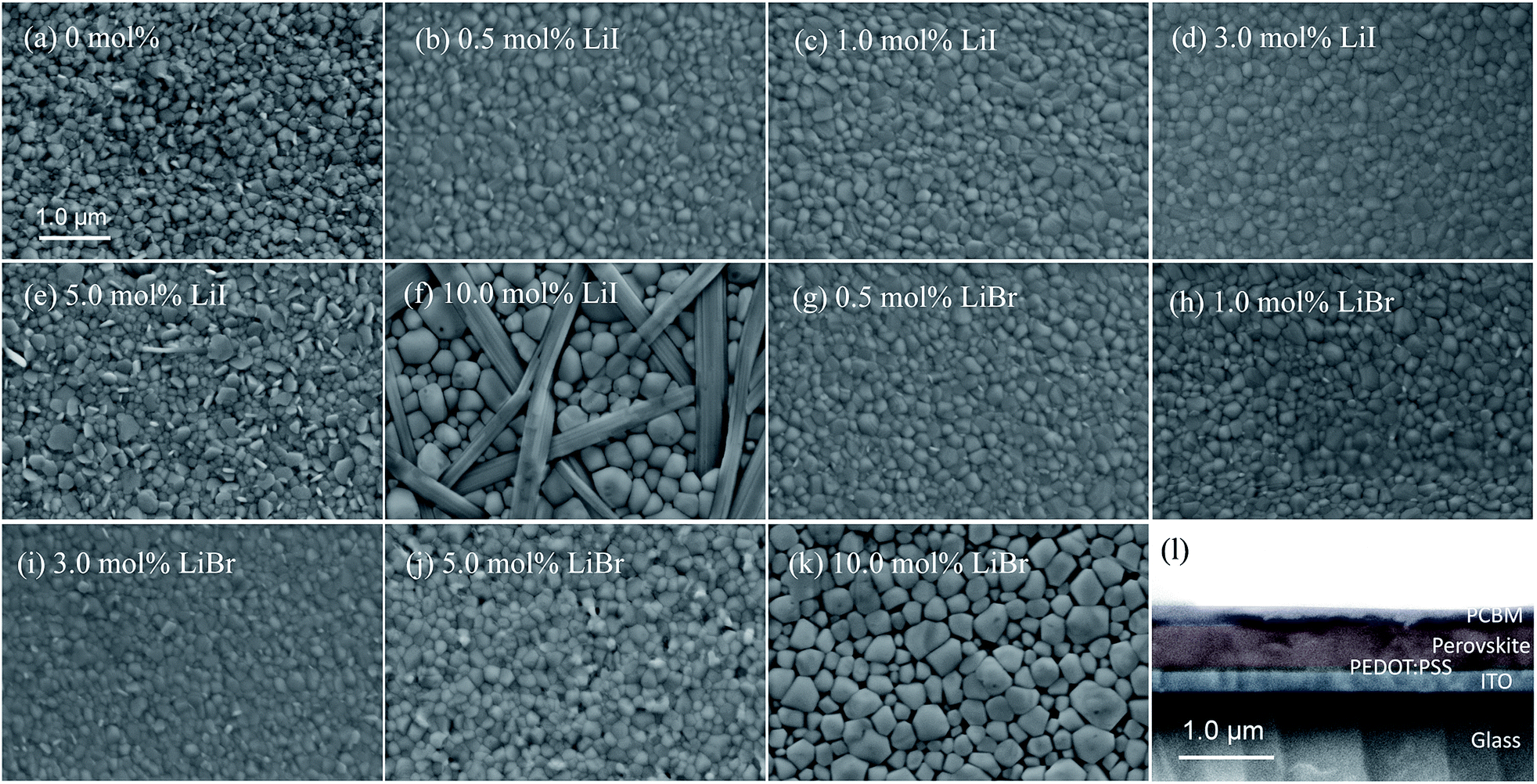 | ||
| Fig. 2 (a)–(k) Top-view SEM images of perovskite thin films based different ratios of Li doping. (l) Cross-section image of perovskite device based on 0.5 mol% LiI doped perovskite. | ||
The planar heterojunction device structure with a configuration of ITO/PEDOT:PSS/perovskite/PCBM/BCP/Ag was used. Current density (J)–voltage (V) characteristics of the device fabricated with the same film formation condition has been shown in Fig. 3. The Voc, Jsc, fill factor (FF), and PCE of all devices are summarized in Table 1. As can been seen, the Li incorporation had a large influence on the device performance. The device exhibited a comparable efficiency of 13.1% for pristine thin film with Jsc, Voc, and FF of 19.6 mA cm−2, 0.93 V, and 0.72, respectively. The 0.5 mol% LiI doped MAPbI3 showed slight increase in PCEs due to enhanced Jsc and Voc, indicating that the impurity threshold limit of the films was 0.5% molar ratio. The corresponding Jsc, Voc, FF and PCE were 20.1 mA cm−2, 0.97 V, 0.73, and 14.2%, respectively. When the doping ratio increased to and 1.0 mol%, and even up to 5 mol%, Jsc and FF gradually reduced. The resulting PCE also decreased to 13.0%, 8.7% and 5.4% for 1%, 3% and 5% molar ratio doped film, respectively. The lower Jsc and FF indicated a high series resistance (Rs) and large charge recombination in the device, which may be due to Li-induced charge traps in the thin film that quenched the photo-generated charge carriers. The PCE of MAPbI3 devices further decreased to 4.8% for the devices with 10% molar doping ratio of samples. And the decrement of PCE was reflected by a reduction of Voc due to structure change induced by the Li impurities. The Jsc, Voc, and FF were 10.5 mA cm−2, 0.96 V, and 0.48, respectively.
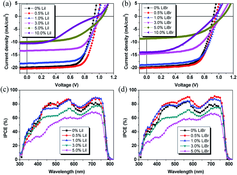 | ||
| Fig. 3 J–V characteristics of different LiI (a) and LiBr (b) doped perovskite thin film devices. IPCE spectra of perovskite solar cells based on different LiI (c) and LiBr (d) dopants. | ||
| Conditions | Jsc (mA cm−2) | Voc (V) | FF | PCE (%) | Rs (Ω cm2) |
|---|---|---|---|---|---|
| PbI2, control | 19.6 ± 0.2 | 0.94 ± 0.02 | 0.73 ± 0.02 | 13.1 ± 0.5 | 3.66 |
| LiI (0.25 mol%) | 19.8 ± 0.2 | 0.95 ± 0.02 | 0.74 ± 0.02 | 13.8 ± 0.4 | 2.88 |
| LiI (0.5 mol%) | 20.1 ± 0.2 | 0.97 ± 0.02 | 0.74 ± 0.02 | 14.3 ± 0.4 | 2.09 |
| LiI (1.0 mol%) | 18.4 ± 0.2 | 0.98 ± 0.02 | 0.73 ± 0.02 | 13.0 ± 0.4 | 2.25 |
| LiI (3.0 mol%) | 13.4 ± 0.3 | 1.03 ± 0.03 | 0.65 ± 0.03 | 8.7 ± 0.6 | 2.47 |
| LiI (5.0 mol%) | 9.9 ± 0.4 | 1.04 ± 0.03 | 0.51 ± 0.04 | 5.4 ± 0.8 | 2.74 |
| LiI (10.0 mol%) | 10.5 ± 0.5 | 0.96 ± 0.04 | 0.50 ± 0.06 | 4.8 ± 0.9 | 3.97 |
| LiBr (0.5 mol%) | 20.3 ± 0.2 | 0.97 ± 0.02 | 0.73 ± 0.02 | 14.1 ± 0.3 | 2.13 |
| LiBr (1.0 mol%) | 18.8 ± 0.2 | 0.98 ± 0.02 | 0.74 ± 0.02 | 13.5 ± 0.4 | 2.48 |
| LiBr (3.0 mol%) | 14.6 ± 0.3 | 1.03 ± 0.02 | 0.68 ± 0.02 | 9.9 ± 0.6 | 2.94 |
| LiBr (5.0 mol%) | 10.8 ± 0.4 | 1.05 ± 0.03 | 0.60 ± 0.04 | 5.3 ± 0.7 | 3.69 |
| LiBr (10.0 mol%) | 13.9 ± 0.4 | 0.95 ± 0.04 | 0.49 ± 0.05 | 6.2 ± 0.8 | 4.76 |
It is believed that proper Br doping could stabilize the Li doped perovskite, probably due to its decreased atomic radius of Br compared to I, which can reduce the crystal strain, and hence, the stability was enhanced. The beneficial role of Br doping provides a practical approach to further enhance the device performance of PSCs. For LiBr case, the 0.5 mol% doped perovskite thin film enhanced the Jsc and Voc to 20.3 mA cm−2 and 0.97 V, respectively. Hence, the resulting PCE was enhanced to 14.1%. Further increasing the LiBr doping ratio, the Jsc decreased from 19.6 mA cm−2 for MAPbI3 to 18.8 mA cm−2, 14.6 mA cm−2, 10.8 mA cm−2, 13.9 mA cm−2 for Li with a molar ratio of 1%, 3%, 5%, and 10%, respectively. The Voc increased from 0.93 V for MAPbI3 to 0.98 V, 1.03 V, 1.05 V, and 0.95 V for Li with a molar ratio of 1%, 3%, 5%, and 10% molar ratio, respectively. The FF decreased to 0.66, 0.58, 0.47 for 3%, 5%, and 10% molar ratio, respectively, due to increased leakage current and charge recombination. The resulting PCE values were 13.5% (1.0 mol%), 9.9% (3 mol%), 5.3% (5 mol%), and 6.2% (10 mol%), respectively. Compared to LiI dopant, the devices with LiBr dopant exhibited higher Jsc which might be ascribed to the improved charge carrier transport and reduced charge recombination induced by impurities-related traps. In order to understand the Li doping effect on the photovoltaic performance of the PSCs, the Rs of the devices was obtained from the J–V curves. The Rs was 3.66 Ω cm2 for the pristine perovskite film based device. It decreased to 2.09 Ω cm2 and 2.13 Ω cm2 for the devices with 0.5 mol% LiI and LiBr doped CH3NH3PbI3, respectively. The steady-state PCE outputs at the maximum power point as a function of time were also checked. As shown in Fig. S4,† the stabilized PCEs were 13.2%, 14.3%, and 14.5% for pristine, 0.5 mol% LiI, and 0.5 mol% LiBr doped perovskite, respectively. This indicates that the device results are stable and reliable.
The effect of Li incorporation was also tested by internal photo-electron conversion efficiency (IPCE) measurements. It is known that the IPCE spectra could provide the information on the components primarily responsible for converting absorbed photos to the collected electrons and holes. As shown in Fig. 3c and d, it could be observed that proper Li amount could enhance the IPCE. The integrated Jsc were 19.8 mA cm−2 and 20.5 mA cm−2 for 0.5 mol% LiI and LiBr doped perovskite device, respectively. When the Li doping ratio increased to above 1.0 mol%, the intensity decreased a lot due to the reduced conversion efficiency. This is slightly different from the observed absorption spectra which showed similar absorption for both thin films due to relatively small change in the absorption spectra by this small amount of Li doping.
In order to further elucidate the Li doping effect on the electronic structure of the MAPbI3, UPS measurement was performed on the pristine perovskite and 10% molar ratio of Li doped perovskite composite. The UPS energy levels have been shown in Fig. 4. The secondary electron cutoff of the pristine perovskite film prepared on ITO substrate was located at 17.1 eV, and the valence band maximum was located at 1.6 eV. Since the energy band of the perovskite was about 1.58 eV, it can be concluded that the Fermi level lay close to conduction band edge of the perovskite, indicating an n-type characteristics of the perovskite material. After incorporating Li into the perovskite structure, the secondary electron cutoff slightly shifted by 0.32 eV and 0.38 eV towards the higher binding energy region, indicating an upshift of the Fermi level of about 0.32 eV and 0.38 eV for 10 mol% LiI and 10 mol% LiBr, respectively. The large Fermi level shift indicated an increased electron density for the Li doped MAPbI3. And this low performance might be due to the poor junction between MA1−xLixPbI3 and PCBM in the solar cell device. Anyway, we achieved a highly n-doped perovskite MA1−xLixPbI3, and applied it in the perovskite solar cell. And it is expected that the solar cell efficiency could be further improved by choosing spiro/MA1−xLixPbI3 system due to favorable energy level alignment.
 | ||
| Fig. 4 UPS spectra of perovskite thin films without and with Li dopants. | ||
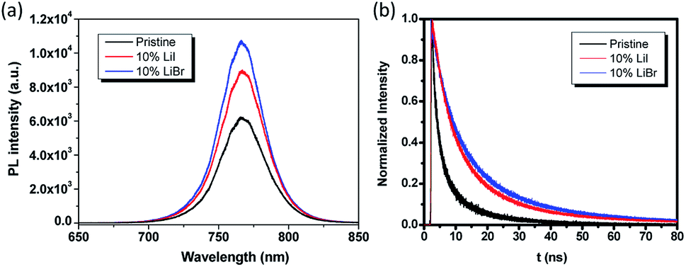
To investigate the photophysical process associated with the Li in the perovskite phase, steady-state photoluminescence (PL) and time-resolved PL measurements were carried out on these thin films. From the steady-state PL, it could be observed that the Li incorporation slightly increased the PL intensity. Time-resolved PL was performed to probe the carrier lifetime of perovskite films prepared on glass substrates. Detailed information about the samples preparation, measurement, and fitting methodology can be found in the experimental part. The PL lifetime of the samples was fitted with a bi-exponential decay function which included a fast decay and a slow decay process. Generally, the radiative electron–hole recombination occurs by two different pathways with two different time scales contributing to the PL decay curves. The PL decay spectra of the samples are shown in Fig. 5b, and the related parameters are summarized in Table 2. The fast decay lifetimes of the pristine perovskite film, 10 mol% LiI doped perovskite film and 10 mol% LiBr doped perovskite film were 1.93 ns, 3.5 ns and 5.0 ns, respectively, and the corresponding slow decay lifetimes of these three samples were 7.74 ns, 21.0 ns, and 31.8 ns, respectively. We have observed a larger PL yield and slower carrier lifetime in the Li doped samples, indicating a decreased nonradiative decay rate, which was likely due to a reduced defect density that suppressed nonradiative recombination.
 | ||
| Fig. 5 Steady-state PL and time-resolved PL spectra for pristine and Li doped perovskite thin films on glass substrates. | ||
| Fraction 1 | τ1 (ns) | Fraction 2 | τ2 (ns) | τave (ns) | |
|---|---|---|---|---|---|
| 0% | 0.47 | 1.93 | 0.53 | 7.74 | 6.68 |
| 10% LiI | 0.61 | 3.5 | 0.39 | 21.0 | 17.34 |
| 10% LiBr | 0.73 | 5.0 | 0.27 | 31.8 | 23.73 |
These results can be further supported by femtosecond transient absorption spectroscopy and pump–probe measurements. Femtosecond transient absorption spectroscopy was performed to study the electron dynamics under excitation of femtosecond laser pulses with wavelength centered at 500 nm, pulse duration of 100 fs and repetition rate of 500 Hz. Fig. 6a–c showed the transient absorption spectra of each films at different time delays. The transient absorption spectra of different perovskite films displayed similar profiles with two major features, a transient bleaching band and a photo-induced absorption band, indicating depopulating of the ground state and the presence of charge carriers. The LiBr doped perovskite film exhibited the highest transient bleaching intensity compared to the other two counterparts, while the pristine perovskite film showed the lowest intensity, which was consistent with the steady-state and time-resolved PL measurements, as the transient bleaching signal originated from the stimulated emission of the samples.
 | ||
| Fig. 6 Transient absorption spectra of for pristine perovskite film (a), LiI doped perovskite film (b), and LiBr doped perovskite film (c) under 500 nm excitation. (d) Single wavelength dynamics probed at 720 nm for different perovskite films. | ||
To monitor the evolution of the carriers upon optical excitation, the single wavelength dynamics probed at 720 nm were shown in Fig. 6d, giving a carrier lifetime of 176 ± 4 ps, 205 ± 8 ps and 305 ± 10 ps for pristine perovskite film, LiI doped perovskite film, and LiBr doped perovskite film, respectively. The presence of excess Li dopants led to rapid charge recombination, as evidenced by the rapid decay of the pristine perovskite film. While 10 mol% LiI or LiBr doped perovskite film could reduce the amount of charge recombination at long timescales. The results of transient absorption spectroscopy and pump–probe measurements provided further support for the results and discussion in the previous sections.
Experimental
Materials and chemicals
Patterned indium tin oxide (ITO) glass substrates (10 Ω □−1) were supplied by NSG group. Poly(3,4-ethy-lenedioxythiophene) poly(styrenesulfonate) (PEDOT:PSS, Clevios P VP Al 4083) was purchased from Heraeus Holding GmbH. Methylammonium iodide (MAI) was obtained from Dyesol Ltd. [6,6]-Phenyl-C61-butyric acid methyl ester (PCBM) was bought from Nano-C Inc. Other materials, including lead(II) iodide (PbI2, 99.9% purity), lithium iodine (LiI, 99.999% purity, anhydrous), lithium bromide (LiBr, 99.999% purity, anhydrous), dimethyl sulfoxide (DMSO, anhydrous, ≥99.9% purity), γ-butyrolactone (GBL, ≥99% purity), chlorobenzene (anhydrous, 99.8% purity), toluene (anhydrous, 99.8% purity) were supplied by Sigma-Aldrich. All materials were used as received without further purification.Fabrication and characterization of perovskite solar cells
ITO glass substrates were cleaned sequentially in detergent, deionized water, acetone, and isopropanol by sonication for 20 min each. After drying under N2 stream, substrates were further treated with UV–ozone for 15 min. A PEDOT:PSS layer with a thickness of ∼40 nm was prepared by spin coating PEDOT:PSS on ITO substrates at 7000 rpm for 1 min and subsequently annealed at 140 °C for 15 min in air. The substrates with PEDOT:PSS were then transferred into a glove box filled with highly pure N2. The perovskite layer was formed by spin coating a solution consisting 1.4 M PbI2 and 1.4 M MAI + LiI (or LiBr) in co-solvent of DMSO![[thin space (1/6-em)]](https://www.rsc.org/images/entities/char_2009.gif) :GBL (3:7 vol. ratio) at 1000 rpm for 20 s, and then at 5000 rpm for 60 s. After 45 s of the start of the spin coating, 200 μl toluene was dripped. Then, they were annealed at 100 °C for 10 min. The thickness of the perovskite thin films was around 280 nm. The PCBM layer with a thickness of about 60 nm was deposited by spin coating a chlorobenzene solution of 20 mg mL−1 PCBM at 1500 rpm for 40 s. The devices were completed by thermally deposition 100 nm-thick Ag in a vacuum of <1 × 10⁻⁶ torr. Each device had an area of 0.075 cm2. The photovoltaic performance of the PSCs was tested in air with a computer-programmed Keithley 2400 source/meter and a Newport'sOriel class A solar simulator which simulated the AM1.5 sunlight with energy density of 100 mW cm−2 and was certified to the JIS C 8912 standard. Incident photon-to-current conversion efficiencies (IPCEs) of PSCs were measured with a 300 W xenon lamp (Oriel 6258) and a Cornerstone 260 Oriel 74125 monochromator.
:GBL (3:7 vol. ratio) at 1000 rpm for 20 s, and then at 5000 rpm for 60 s. After 45 s of the start of the spin coating, 200 μl toluene was dripped. Then, they were annealed at 100 °C for 10 min. The thickness of the perovskite thin films was around 280 nm. The PCBM layer with a thickness of about 60 nm was deposited by spin coating a chlorobenzene solution of 20 mg mL−1 PCBM at 1500 rpm for 40 s. The devices were completed by thermally deposition 100 nm-thick Ag in a vacuum of <1 × 10⁻⁶ torr. Each device had an area of 0.075 cm2. The photovoltaic performance of the PSCs was tested in air with a computer-programmed Keithley 2400 source/meter and a Newport'sOriel class A solar simulator which simulated the AM1.5 sunlight with energy density of 100 mW cm−2 and was certified to the JIS C 8912 standard. Incident photon-to-current conversion efficiencies (IPCEs) of PSCs were measured with a 300 W xenon lamp (Oriel 6258) and a Cornerstone 260 Oriel 74125 monochromator.
Materials characterizations
X-ray diffraction (XRD) spectra were acquired using a Bruker D8 Advance XRD Instrument. UV-vis absorption spectra were recorded with a Shimadzu UV-1800 spectrophotometer. Electron scanning microscopic (SEM) images were obtained with a Zeiss Supra-40 SEM. Film thickness was determined by a surface profilometer (KLATencor, Alpha-Step IQ). Ultraviolet photoelectron spectroscopy (UPS) spectra were acquired with a VG ESCA 220i-XL system. The UV source used was a He discharge lamp with a photon energy of 21.22 eV. Photoluminescence spectra were collected on an Edinburgh Instruments FLS920 spectrofluorometer, and the excitation wavelength was 633 nm. For the time-resolved photoluminescence, the excitation source was a diode laser (NanoLED) working at a repetition rate of 10 MHz, with wavelength of 438 nm and pulse duration of ∼260 ps. The scattering of excitation light was eliminated by a two-600 nm long pass filter. Photoluminescence was collected and detected by an avalanche photon diode (Micro photon device, PicoQuant) attached to a time-correlated single photon counting card (TCSPC PicoHarp 300, PicoQuant). For the femtosecond transient absorption, the laser pulses generated from a mode-locked Ti:Sapphire oscillator seeded regenerative amplifier working at 800 nm with repetition rate of 1 kHz and pulse duration of 50 fs. The 800 nm laser was splitted into two portions. A larger portion pumped an optical parametric amplifier (TOPAS, Light conversion) and generated the pump beam with wavelength of 500 nm. A residual portion generated white light continuum in a 1 mm sapphire plate. The fluctuation of both pump and probe beams were cancelled out. The pump beam was focused onto the film with a beam size of 300 μm and overlapped with a smaller diameter probe beam ∼100 μm. The time delay of the pump and probe laser pulse was varied by a computer controlled translational stage (Newport, ESP300). The pump beam was modulated by an optical chopper at a frequency of 500 Hz. The variation transmittance at selected probe wavelength was recorded as a function of time delay between pump and probe pulses.Conclusions
In conclusion, we have studied the Li incorporation effect on the CH3NH3PbI3 perovskite film formation, film crystallinity and morphology, charge carriers dynamic, as well as the solar cell device performance. It was found that within the threshold limit of 1.0 mol% of Li, the Li had positive effect on the perovskite film properties and corresponding device performance. However, solar cell devices exhibited significantly reduction upon 3 mol% incorporation. Meanwhile, after further increasing the ratio to 10 mol%, the film totally changed, and the charge carrier lifetime was significantly enhanced compared to pristine film due to increased crystal size and reduced crystal defects. The Li doping mechanism was discussed, and it was thought to contain two different doping mechanisms. One is interstitial doping at much lower doping ratio, and another is substitutional doping for MA cation at higher doping ratio. This study highlights the possibility of inorganic cation doping as an efficient route for crystal construction and defect density control.Conflicts of interest
There are no conflicts to declare.Acknowledgements
This work was financially supported by National Natural Science Foundation of China (61604119, 61704131), Natural Science Foundation of Shaanxi Province (2017JQ6002, 2017JQ6031), the Fundamental Research Funds for the Central Universities, and Young Talent fund of China Association for Science and Technology.Notes and references
- M. M. Lee, J. Teuscher, T. Miyasaka, T. N. Murakami and H. J. Snaith, Science, 2012, 338, 643–647 CrossRef CAS PubMed.
- A. Mei, X. Li, L. Liu, Z. Ku, T. Liu, Y. Rong, M. Xu, M. Hu, J. Chen, Y. Yang, M. Gratzel and H. Han, Science, 2014, 345, 295–298 CrossRef CAS PubMed.
- S. D. Stranks, G. E. Eperon, G. Grancini, C. Menelaou, M. J. P. Alcocer, T. Leijtens, L. M. Herz, A. Petrozza and H. J. Snaith, Science, 2013, 342, 341–344 CrossRef CAS PubMed.
- H. Zhou, Q. Chen, G. Li, S. Luo, T.-b. Song, H.-S. Duan, Z. Hong, J. You, Y. Liu and Y. Yang, Science, 2014, 345, 542–546 CrossRef CAS PubMed.
- J. Burschka, N. Pellet, S.-J. Moon, R. Humphry-Baker, P. Gao, M. K. Nazeeruddin and M. Grätzel, Nature, 2013, 499, 316–319 CrossRef CAS PubMed.
- M. Liu, M. B. Johnston and H. J. Snaith, Nature, 2013, 501, 395–398 CrossRef CAS PubMed.
- D. Liu and T. L. Kelly, Nat. Photonics, 2013, 8, 133–138 CrossRef.
- N. J. Jeon, J. H. Noh, Y. C. Kim, W. S. Yang, S. Ryu and S. Il Seok, Nat. Mater., 2014, 13, 897–903 CrossRef CAS PubMed.
- J. Chang, J. Xiao, Z. Lin, H. Zhu, Q.-H. Xu, K. Zeng, Y. Hao and J. Ouyang, J. Mater. Chem. A, 2016, 4, 17464–17472 CAS.
- N. J. Jeon, J. H. Noh, W. S. Yang, Y. C. Kim, S. Ryu, J. Seo and S. Il Seok, Nature, 2015, 517, 476 CrossRef CAS PubMed.
- W.-Q. Wu, D. Chen, W. A. McMaster, Y.-B. Cheng and R. A. Caruso, ACS Appl. Mater. Interfaces, 2017, 9, 31959–31967 CAS.
- J. Chang, Z. Lin, H. Zhu, F. H. Isikgor, Q.-H. Xu, C. Zhang, Y. Hao and J. Ouyang, J. Mater. Chem. A, 2016, 4, 16546–16552 CAS.
- J. Chang, H. Zhu, J. Xiao, F. H. Isikgor, Z. Lin, Y. Hao, K. Zeng, Q.-H. Xu and J. Ouyang, J. Mater. Chem. A, 2016, 4, 7943–7949 CAS.
- Z. Lin, J. Chang, J. Xiao, H. Zhu, Q.-H. Xu, C. Zhang, J. Ouyang and Y. Hao, Sol. Energy Mater. Sol. Cells, 2016, 157, 783–790 CrossRef CAS.
- Z. Zhou, S. Pang, Z. Liu, H. Xu and G. Cui, J. Mater. Chem. A, 2015, 3, 19205–19217 CAS.
- W.-Q. Wu, H.-L. Feng, H.-Y. Chen, D.-B. Kuang and C.-Y. Su, J. Mater. Chem. A, 2017, 5, 12699–12717 CAS.
- Z. Lin, J. Chang, H. Zhu, Q. H. Xu, C. Zhang, J. Ouyang and Y. Hao, Sol. Energy Mater. Sol. Cells, 2017, 172, 133–139 CrossRef CAS.
- J. T.-W. Wang, Z. Wang, S. Pathak, W. Zhang, D. W. DeQuilettes, F. Wisnivesky-Rocca-Rivarola, J. Huang, P. K. Nayak, J. B. Patel, H. A. Mohd Yusof, Y. Vaynzof, R. Zhu, I. Ramirez, J. Zhang, C. Ducati, C. Grovenor, M. B. Johnston, D. S. Ginger, R. J. Nicholas and H. J. Snaith, Energy Environ. Sci., 2016, 9, 2892–2901 CAS.
- NREL—National Renewable Energy Laboratory chart, http://www.nrel.gov/ncpv/images/efficiency_chart.jpg, 2017.
- J. Chang, H. Zhu, B. Li, F. Isikgor, Y. Hao, Q. Xu and J. Ouyang, J. Mater. Chem. A, 2016, 4, 887–893 CAS.
- X. Sun, C. Zhang, J. Chang, H. Yang, H. Xi, G. Lu, D. Chen, Z. Lin, X. Lu, J. Zhang and Y. Hao, Nano Energy, 2016, 28, 417–425 CrossRef CAS.
- N. K. Noel, S. D. Stranks, A. Abate, C. Wehrenfennig, S. Guarnera, A. Haghighirad, A. Sadhanala, G. E. Eperon, S. K. Pathak, M. B. Johnston, A. Petrozza, L. Herz and H. Snaith, Energy Environ. Sci., 2014, 7, 3061–3068 CAS.
- F. Hao, C. C. Stoumpos, R. P. H. Chang and M. G. Kanatzidis, J. Am. Chem. Soc., 2014, 136, 8094–8099 CrossRef CAS PubMed.
- W.-J. Yin, T. Shi and Y. Yan, Adv. Mater., 2014, 26, 4653–4658 CrossRef CAS PubMed.
- A. Dymshits, A. Rotem and L. Etgar, J. Mater. Chem. A, 2014, 2, 20776–20781 CAS.
- J. H. Heo, D. H. Song and S. H. Im, Adv. Mater., 2014, 26, 8179–8183 CrossRef CAS PubMed.
- J. H. Noh, S. H. Im, J. H. Heo, T. N. Mandal and S. Il Seok, Nano Lett., 2013, 13, 1764–1769 CrossRef CAS PubMed.
- P.-W. Liang, C.-C. Chueh, X.-K. Xin, F. Zuo, S. T. Williams, C.-Y. Liao and A. K.-Y. Jen, Adv. Energy Mater., 2015, 5, 1400960 CrossRef.
- L. Dimesso, M. Dimamay, M. Hamburger and W. Jaegermann, Chem. Mater., 2014, 26, 6762–6770 CrossRef CAS.
- J.-W. Lee, D.-J. Seol, A.-N. Cho and N.-G. Park, Adv. Mater., 2014, 6, 4991–4998 CrossRef CAS PubMed.
- S. Pang, H. Hu, J. Zhang, S. Lv, Y. Yu, F. Wei, T. Qin, H. Xu, Z. Liu and G. Cui, Chem. Mater., 2014, 26, 1485–1491 CrossRef CAS.
- N. Pellet, P. Gao, G. Gregori, T.-Y. Yang, M. K. Nazeeruddin, J. Maier and M. Grätzel, Angew. Chem., Int. Ed. Engl., 2014, 53, 3151–3157 CrossRef CAS PubMed.
- G. E. Eperon, S. D. Stranks, C. Menelaou, M. B. Johnston, L. M. Herz and H. J. Snaith, Energy Environ. Sci., 2014, 7, 982 CAS.
- J. K. Nam, S. U. Chai, W. Cha, Y. J. Choi, W. Kim, M. S. Jung, J. Kwon, D. Kim and J. H. Park, Nano Lett., 2017, 17, 2028–2033 CrossRef CAS PubMed.
- F. Wu, J. T. Lee, N. Nitta, H. Kim, O. Borodin and G. Yushin, Adv. Mater., 2014, 27, 101–108 CrossRef PubMed.
- S. a. Haque, T. Park, C. Xu, S. Koops, N. Schulte, R. J. Potter, a. B. Holmes and J. R. Durrant, Adv. Funct. Mater., 2004, 14, 435–440 CrossRef CAS.
- V. Thavasi, V. Renugopalakrishnan, R. Jose and S. Ramakrishna, Mater. Sci. Eng., R, 2009, 63, 81–99 CrossRef.
- W. H. Nguyen, C. D. Bailie, E. L. Unger and M. D. McGehee, J. Am. Chem. Soc., 2014, 136, 10996–11001 CrossRef CAS PubMed.
- Y. Guo, C. Liu, K. Inoue, K. Harano, H. Tanaka and E. Nakamura, J. Mater. Chem. A, 2014, 2, 13827 CAS.
- F. Giordano, A. Abate, J. P. Correa Baena, M. Saliba, T. Matsui, S. H. Im, S. M. Zakeeruddin, M. K. Nazeeruddin, A. Hagfeldt and M. Graetzel, Nat. Commun., 2016, 7, 10379 CrossRef CAS PubMed.
- M. R. Filip, G. E. Eperon, H. J. Snaith and F. Giustino, Nat. Commun., 2014, 5, 5757 CrossRef CAS PubMed.
Footnotes |
| † Electronic supplementary information (ESI) available: XRD spectra, band gap of doped perovskite, steady-state PCE output. See DOI: 10.1039/c8ra01199k |
| ‡ These authors contributed equally to this work. |
| This journal is © The Royal Society of Chemistry 2018 |