
 Open Access Article
 This Open Access Article is licensed under a Creative Commons Attribution-Non Commercial 3.0 Unported Licence
Nanolithography using thermal stresses†
Gangadhar Purohitab,
Deepakab and
Monica Katiyar *ab
*ab
aMaterials Science & Engineering, Indian Institute of Technology Kanpur, UP-208016, India
bNational Centre for Flexible Electronics, Indian Institute of Technology Kanpur, UP-208016, India. E-mail: mk@iitk.ac.in
First published on 29th January 2018
Abstract
Nanometer separation (nanogap) in electrodes is a fundamental requirement for several nanoscale devices having applications in nanoelectronics, nanophotonics, biosensing, nanoporous filters, healthcare and medical diagnostics. Most nanolithography techniques, other than extreme/deep ultraviolet lithography are serial processes, such as e-beam lithography, and therefore not scalable. We demonstrate fabrication of nanogaps in Au electrodes over a large area/wafer in parallel processing mode resulting in high throughput. The proposed technique requires tools that are already available in a typical semiconductor device fabrication facility. The concept involves designing a ceramic/metal multilayer structure which is heated to bring the ceramic under tensile stress, and as a result it develops cracks due to low fracture toughness of the ceramic. The feasibility of this idea was established by calculating thermal stresses in different multilayers when heated to a specified temperature level. At practical temperatures, below 500 °C, the developed tensile stresses are higher than the critical stress needed for fracture. Subsequent to separation in the ceramic layer at the desired location, the underlying metal layer can be wet etched leading to separation in the metal also. For electrode fabrication, a predefined notch in the multilayer structure is used to obtain the nanogap at the desired location. For experimental validation, SiOx/Au/Ti layers on glass and silicon are patterned in I-shaped electrodes using conventional optical lithography. After vacuum annealing and etching, nanogaps in Au electrodes are simultaneously formed across a large area substrate/wafer. The nanoscale gaps formed in the Au electrodes were inspected using optical microscopy, FE-SEM imaging and finally were verified using an electrical isolation test. We achieved nanogaps with dimensions of ∼150–300 nm in Au electrodes on glass substrates.
1. Introduction
Fabrication techniques suitable for manufacturing processes are key to success of nanoelectronics.1,2 Several fabrication methods to make nanostructures in materials have already been demonstrated. These include: mechanically controllable break junction (MCBJ) method,3 electrochemical and chemical deposition,4,5 oblique angle shadow evaporation,6,7 electromigration and electrical breakdown method,8 optical lithography,9,10 focused ion beam (FIB) lithography,11,12 scanning probe lithography (SPL),13,14 electron beam lithography (EBL),15,16 dip pen lithography (DPL),17,18 imprint lithography19 and X-ray lithography.20 Each technique has its strengths and weaknesses in regards to resolution, throughput, scalability and cost. Overall, all of them suffer from one or a combination of following problems – (i) non scalability: technique limited only to laboratories, (ii) throughput: creation of nanogap, device by device, consuming a long time and (iii) use of expensive equipment. Thus far, few studies in literature have focused on scaling up production of nanogap in electrodes for practical electronic applications. Simultaneously fabricating nanogaps in a large number of electrodes in a single manufacturing process remains a challenge.In this work, we demonstrate a technique for realizing a nanogap in electrodes using regular microelectronics processing equipment.21 The other strength of the invention is that it is scalable, a large number of nanogap electrodes can be simultaneously produced in a single processing step over a substrate or wafer. The basic thought behind the technique is that when layers of two materials having dissimilar thermal expansion coefficients are subjected to heating or cooling, one of the layers acquires a tensile stress and is susceptible to cracking, leading to nanogaps. The processing steps involve combination of following processes: (i) deposition of selected materials (having dissimilar thermal expansion coefficient), (ii) patterning the multilayer structure using standard lithography, (iii) subjecting the multilayer structure to thermal cycle that produces crack in one of the layers, (iv) using etching to transfer the crack to another layer. We define preferential locations for cracking by making a notch, thereby localizing the crack in desired location simultaneously at a large number of places on the substrate. Such cracks can be formed in any material. If formed in a metal layer, it will separate the electrodes with a nanometer gap.
Crack formation is mainly considered as material failure and is often focused on how to avoid them in most research, one famous example is interconnects cracking in integrated circuits. However, close investigation on cracking phenomena and its possible applications have demonstrated cracks as useful features for device fabrication,22–25 for growth of nanowires or to form nanochannels,26,27 as a tool for controlled patterning during thin film deposition28 and as microfluidic channels.29,30 There are some published reports on crack based lithography.31–34 Dubois et al. have shown crack junctions defining nanogap in titanium nitride (TiN). They have followed a process where stress build up due to suspended nature of electrodes leads to formation of a crack. To elaborate on the work further, first notched TiN electrode bridges were fabricated using focused e-beam nanolithography technique. The notched TiN electrode bridges were fabricated on top of a sacrificial layer of Al2O3. Upon chemical etching of Al2O3 notched TiN electrode bridge is suspended. At last crack was formed only at notched point of electrode bridges due to local stress build up by the hanging nano-patterned electrode bridges. The technique already uses e-beam lithography and is limited to brittle materials such as TiN electrodes. Cui et al. demonstrated fabrication of suspended narrow bridges of Au thin films using e-beam lithography and milling of underneath SiO2 layer (below the notched Au electrodes) by focused ion beam (FIB). The nanogap junction is created in this structure due to the grain boundary cracking of Au ultrathin film. Both technique use e-beam lithography and FIB milling, both are expensive and have low throughput. FIB milling also causes contamination at the nano-junction. In summary, the earlier crack based lithography techniques are using expensive equipment and are not scalable to large area.
Our proposed technique21 has potential for mass production of nanogap electrodes in a parallel processing mode using micrometer scale photolithography process. Designing multilayer structure using materials with different thermal expansion coefficient is key to our idea. The basic thought behind the technique is that when layers of two materials having dissimilar thermal expansion coefficients are subjected to heating or cooling, one of the layers acquires a tensile stress and is susceptible to cracking, leading to nanogaps. But this cracking would be uncontrolled. Hence, another aspect of our invention is to do parallel processing by defining preferential locations for cracking, thereby localizing the crack in desired locations, simultaneously at a large number of places on a substrate. In this work, gold is selected as electrode material, it has several applications due to good conducting properties, stability and compatibility with industrial semiconductor processes. The paper is divided into two parts, in the first part simulation results are presented that predict that there is enough thermal stress generated in the structure of multilayered materials to initiate a crack that leads to creation of a nanogap. In the second part we present experimental verification of the concept. We have implemented the idea as a proof-of-concept on 1 × 1 square inch substrate containing 256 numbers of devices in an array. We have patterned features with ∼150–400 nm dimensions using our research laboratory based photolithography facility capable of ∼2 μm patterning. In principle, technique can be improved further by using improved processing conditions.
2. Results and discussion
2.1 Simulations based test of feasibility
The state of stress is calculated by Abaqus (details of the model can be found in the ESI section†). We first verify our calculations, that is, the meshing and model selection, by comparing the computed results in situations where an analytical solution may exist. For example, consider sample geometry and the coordinate system shown in Fig. 1, in which a thin layer of Au film is atop a thick glass substrate.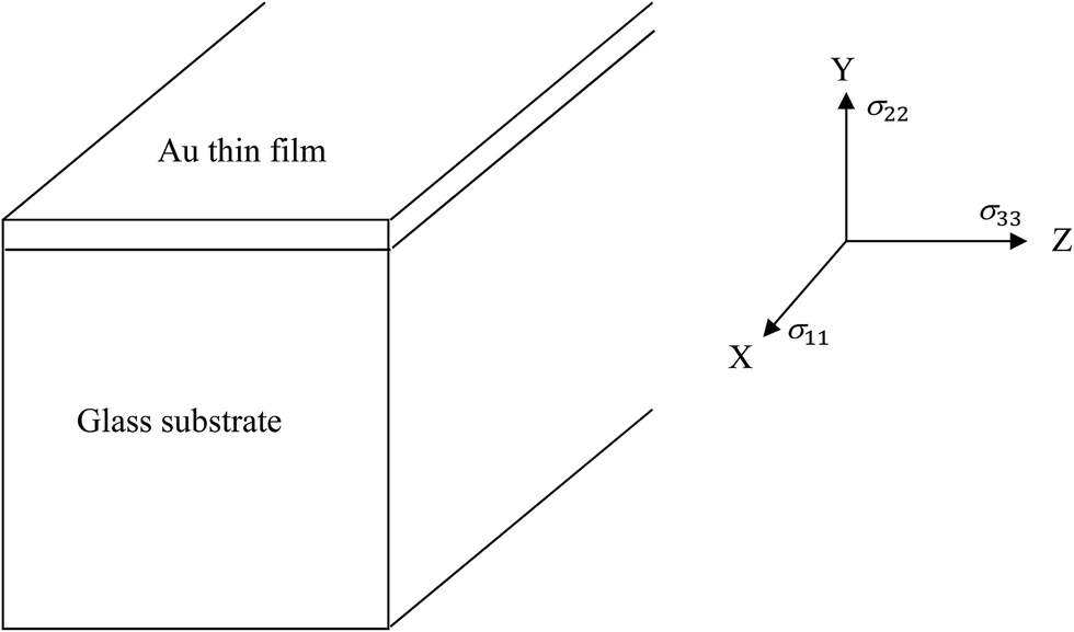 | ||
| Fig. 1 Schematic diagram showing relevant stress components in the film and substrate. | ||
All materials are assumed isotropic, hence only two parameters are needed for stress calculation, namely modulus of elasticity (E) and Poisson's ratio (ν), along with the coefficient of thermal expansion (CTE) for each material. These are taken from literature. Table 1 lists the values used in the simulations for borosilicate glass, Au, Ti and SiO2, the last two materials being present in the later calculations. Borosilicate glass is taken as thick substrate during calculation; hence all parameters pertaining to bulk values are used. Its elastic modulus, Poisson's ratio and CTE are reported as 63 GPa, 0.2 and 3.25–3.3 × 10⁻⁶/K.35,36
| Material properties | Borosilicate glass | Titanium film (Ti) | Gold thin film (Au) | Silicon oxide (SiO2) |
|---|---|---|---|---|
| Modulus of elasticity, E (GPa) | 63 | 115 | 41 | 68 |
| Poisson's ratio, ν | 0.20 | 0.32 | 0.42 | 0.17 |
| Thermal expansion co-efficient, α (K−1) | 3.3 × 10⁻⁶ | 8.41 × 10⁻⁶ | 13.9 × 10⁻⁶ | 0.55 × 10⁻⁶ |
However, for Au the value of modulus of elasticity varies from that of bulk gold to its thin film form. The Young's modulus of gold thin film (18–73 nm) is reported in the range of 69.1 ± 2.6 GPa by Salvadori et al.37,38 and Vaz et al.39 Some groups40,41 have measured Au thin film elastic modulus as 73 GPa and bulk gold elastic modulus as 79–80 GPa. Using surface micro machined beam structures, modulus of elasticity is measured between 35.2–43.9 GPa for a thermally evaporated gold film of 100 nm thickness.42 The elastic modulus E for an Au film of thickness 150 nm is measured as 51.4 ± 10.6 GPa by Sharpe et al.40 In order to estimate the order of stress generated during heating or cooling, we have taken a middle value of 41 GPa for elastic modulus of Au. Poisson's ratio and CTE for Au are reported as 0.42 and 14.2–14.7 × 10⁻⁶/K, respectively.41,43 Similarly, the material properties for Ti and SiO2 thin films are taken from ref. 44.
Reverting back to the calculations of stress in a 50 nm gold layer atop thick glass, this case can be regarded as plane stress condition with biaxial loading in which σ22 is zero. Under the assumption of isotropic properties, σ11 = σ33 = σAu. This stress is known analytically to be equal to 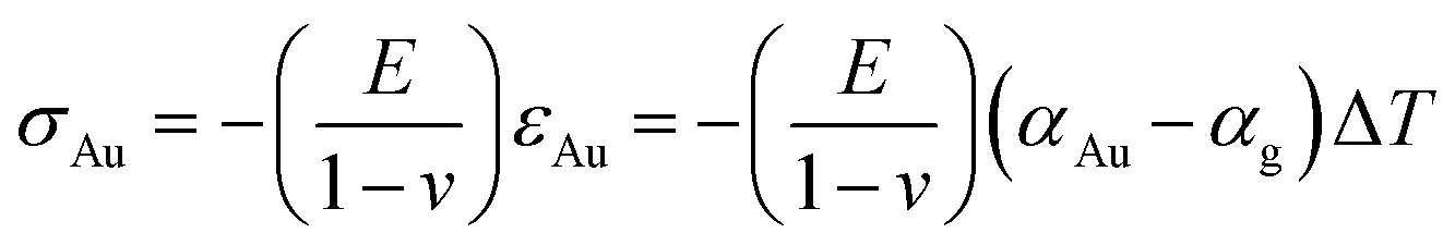 .48 For a ∣ΔT∣ = 273 K, the stress in the gold film amounts to 204.5 MPa. Our calculations using Abaqus for cooling from 573 to 300 K leads to a tensile stress and for heating from 300 to 573 K to a compressive stress. The stress in both cases is 204.5 MPa and spatially uniform, which compares well with the analytical result, thus validating our calculations.
Now, we examine a structure in which a thin adhesion layer of Ti (10 nm) is sandwiched between glass and a gold layer (50 nm), as will be required in experiments and indicated in Fig. 2. In this figure, the two metal layers are in I-shape that provides two pads (for eventual electrical probing). The central metal line is to be separated by cracks; a notch is provided to guide, that is, localize the crack formation to a desired position. The symmetry of the domain requires simulation only in quarter of the structure as also shown by dotted region in the same figure.
 | ||
| Fig. 2 The substrate is glass (grey) on top of which are 10 nm Ti adhesion layer (violet) and 50 nm Au (yellow). The dimensions are included but the figure is not to the scale and notch is characterized by d, t and θ; the dotted region of glass is the calculation domain. | ||
We calculate the tensile and compressive stresses in Au thin film due to heating or cooling. For the case of cooling, we assumed that the metal films are deposited on glass at some high temperature, maximum value of which in the calculation is 500 °C. At the deposition temperature, the Au film is stress free. Then film on glass is cooled to 27 °C. Due to mismatch of thermal expansion coefficient between the two layers, Au having greater thermal expansion coefficient, a tensile stress field is created in the bilayer structure. It may be noted that since the properties are isotropic and taken to be temperature independent in the calculations, it does not matter what the absolute temperatures are; rather, only the amount of cooling is important. Hence, it is equally applicable that the film is deposited at 27 °C and then heated up. Thus, only ΔT, the amount of cooling or heating, should be taken as relevant rather than the actual deposition temperature. Further, it may be noted, that due to presence of a notch, now in a circular region around the notch, a fine mesh of larger number of elements is used.
Upon cooling the deposited metal films by a fixed amount, a tensile stress develops. In Fig. 3, we show the tensile stress σ11 (whose value determines whether a crack will form in the Au film) in the notch region in gold as a function of amount of cooling (or heating). In Fig. 4, for a case where metal is deposited at 500 °C and then cooled to 27 °C, that is by an amount of 473 °C, we show that a tensile stress develops in the gold film, while the thick substrate, the glass, is in slight compression. The stress is mostly uniform in the metal, with only slightly increased values in the notched region. Thus in Fig. 3, σ11 stress, tensile in metal upon cooling and compressive upon heating, reduces as the amount of cooling or heating is reduced. The question we address by these calculations is whether a practical ΔT of cooling (or heating in another case later) is available to propagate a crack in the film that is to be patterned. Thus, we also approximate the critical stress needed for fracture from the fracture toughness data.
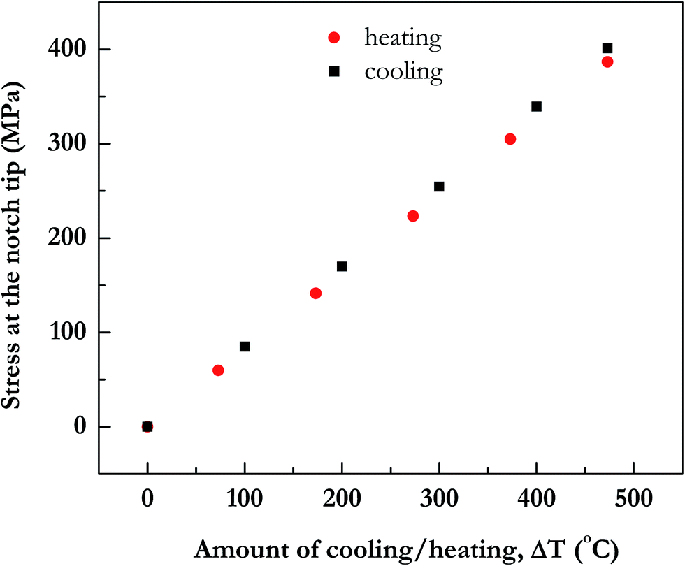 | ||
| Fig. 3 Thermal stress σ11 in gold film at notch tip upon heating or cooling. Red symbols denote amount of temperature increase on heating and black symbols denote amount of decrease in temperature on cooling. This is for a case where wedge to wedge separation (d) is 7 μm, notch depth (t) is 3.5 μm and notch angle (θ) is 40°. | ||
 | ||
| Fig. 4 Thermal stress in thick glass/Ti (10 nm)/Au (50 nm). The metal film is in tension (yellow) while the glass is in compression (blue) after cooling from 500 to 27 °C. | ||
Since only the metal film is in tension, critical stresses that lead to cracking are expected only in the metal. Within metal too, Ti is very thin (only to promote adhesion of gold to glass) and adjacent to glass. Hence, maximum stress is available in the gold film. Its value after cooling by 473 °C (that is, to 27 °C), is 401 MPa. Crack formation will usually take place when stress value of a material is more than the critical stress for fracture. But gold normally has ductile behaviour and plastically deforms, and does not easily crack although stress value is more than the critical stress of fracture.
For simplicity in approximation, we estimate the critical stress for crack formation in Au film using 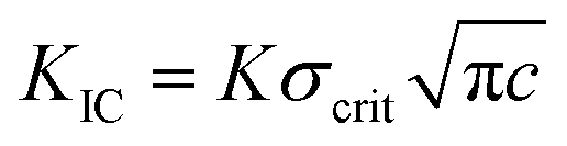 .49 In this, K is taken as 1 and we assume existing crack of length (c) in range 0.2 to 1 μm; note that the approximation is adequate because the purpose is only to estimate if the thermal stress is in similar range as the critical stress and hence motivating physical experimentation. Inclusion of a notch helps in creating a pre-existing crack in the bridge that needs to be propagated across the bridge. In Table 2, for column on Au, based on the fracture toughness, KIC of 0.5 MPa m1/2 (0.45 MPa m1/2 in ref. 50 and 0.7 MPa m1/2 in ref. 51), critical stress is calculated for two assumed values of c and they are compared with the thermal stress computed for ΔT = 473 °C. Clearly, with presence of submicron notches, cooling by temperatures on the order of 300–500 °C, forming a crack in gold film may be feasible.
| Crack length, μm | Au | SiO2 | |||
|---|---|---|---|---|---|
| σcrit,Au (MPa) for KIC = 0.5 MPa m1/2 | Computed σ11 (MPa) in the notched region | σcrit (MPa) for KIC = 0.92 MPa m1/2 | σcrit (MPa) for KIC = 0.09 MPa m1/2 | Computed σ11 (MPa) in the notched region | |
| 0.2 | 630.84 | 401 (ΔT = 473 °C) | 1160.75 | 113.55 | 137 (ΔT = 273 °C), 238 (ΔT = 473 °C) |
| 1 | 282.12 | 519.0 | 50.78 | ||
However, there are difficulties in this approach. In most cases, metals are not deposited at high temperatures. Hence, margin for cooling by such amounts are not practical. Second, the same substrate, glass or silicon, may have multiple metals deposited on it. That would require cooling by different amounts to cause crack propagation in the metal. Hence, a process is needed that is preferably done in heating, rather than cooling, as heating by 400–500 °C is practical and it should be independent of the metal that needs to be patterned.
Hence an alternative idea involves depositing a ceramic thin film of lower thermal expansion coefficient than metal, such as SiO2 or Si3N4, on top of the Au layer. In this case, upon heating, it is the ceramic film that will be in tensile stress and the metal film under compression. Thus cracking would happen in the brittle ceramic film. Once the ceramic film cracks, a metal etching step (dry or wet) would remove the metal in cracked region while the ceramic film protects the remaining metal, leading to a separation in the metal. In effect, the ceramic film also acts as a hard mask during etching.
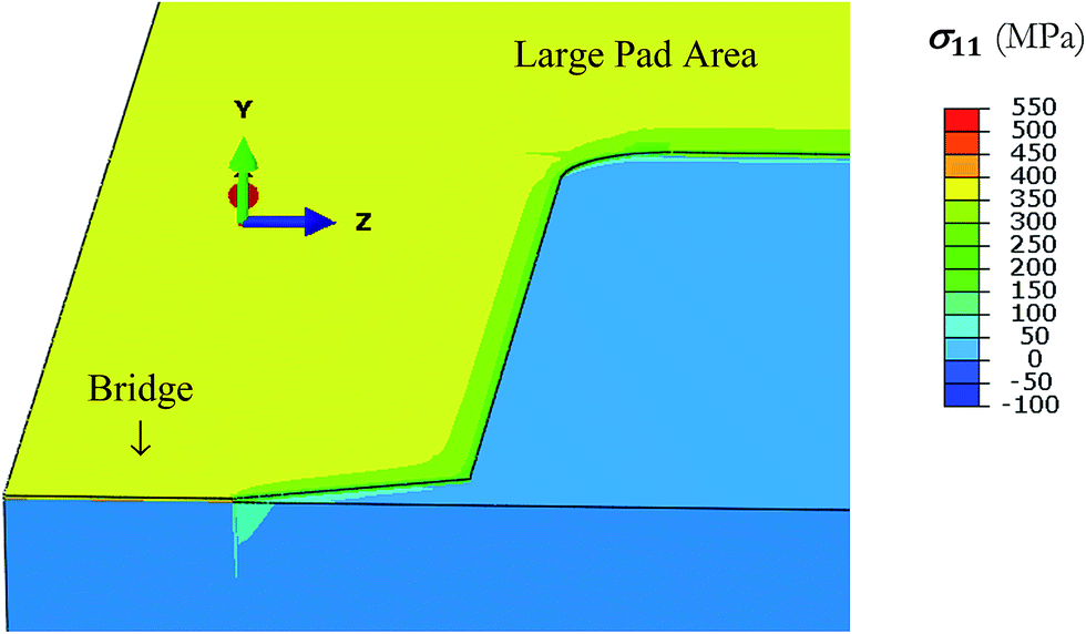
Therefore we again calculate the stress at the notched region in a stack glass/Ti/Au/SiOx. The geometry remains the same as in Fig. 2, except an additional SiOx layer of 300 nm, sufficient to provide etch resistance later when Au and Ti are being etched, is found on top of gold. In this case, the film stack on glass is heated from room temperature to different annealing temperatures. Stress distribution in the stack, assuming films are deposited at 27 °C and then heated up to 500 °C, is shown in Fig. 5. Tensile stress is indicated by orange color in SiOx film, compressive stress is indicated by blue color in Ti/Au metal layers and green color (mild compression) in thick glass substrates. In Fig. 5b, red color indicates stress concentration at the notch tip. The stresses developing in SiOx film are tensile in nature during heating because of co-efficient of thermal expansion difference between SiOx and Au films.
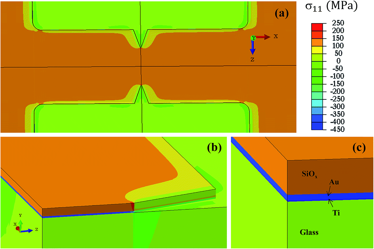 | ||
| Fig. 5 Stresses generated on multilayered thin films of Ti/Au/SiOx when heated to 500 °C. (a) Top view of stress map, (b) side view of stress distribution in one quadrant of the structure, with red color indicating stress concentration at the notch top and (c) a magnified view of thin films stacking, showing compressive (blue) stress in metal layers. Also, now glass is in slight tension. | ||
In Fig. 6, the tensile stress in SiOx film at the notch is plotted. Amount of stresses developed increase with the increase in annealing temperature. For the sake of completeness, we have also plotted in the same figure data for compressive stress in SiOx film if it were cooled and as expected they turn out to be similar in magnitude as tensile stress for equivalent heating.
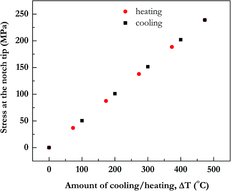 | ||
| Fig. 6 Thermal stress σ11 in SiOx film at notch tip upon heating or cooling. Red symbols denote amount of temperature increase on heating and black symbols denote amount of decrease in temperature on cooling. The notch parameters in the simulation are the same as in Fig. 3. | ||
We again determine if the tensile stress so generated in SiOx film during heating is sufficient to cause crack opening. Literature52,53 reveals value of fracture toughness, KIC, of SiO2 films in the range of 0.09–0.92 MPa m1/2. Accordingly, as in Table 2, critical tensile stress on SiO2 is calculated for two values of both KIC and c and they are compared with computed tensile stress for two values of ∣ΔT∣, 273 and 473 °C. Heating the metal/SiOx films by 300–500 °C is much more convenient and as seen from Table 2, for lower values of KIC and submicron cracks, this process may be feasible.
Since the calculations only establish the feasibility, we also demonstrate formation of cracks through experimentation, first on glass and subsequently on silicon as well, the two substrates which are commonly used.
2.2 Demonstration of electrically isolated electrodes by crack formation
The proposed idea of causing separation in metal line by thermal stress cracking was first verified on glass substrate. At first, only Au and Ti layers were deposited, both at room temperature, as in Fig. 2 (after patterning), which potentially can be directly cracked when cooled. However, unfortunately, the amount of cooling is limited; in our case using liquid nitrogen provides cooling for room temperature deposited Ti/Au layers only by an amount approximately 225 °C. Further, the attempts with this approach failed as the glass itself cracked in liquid nitrogen. Hence, this approach was abandoned and we deposited silicon oxide on top of the metal, for cracking the oxide by heating. In this approach also, we first made patterns of Ti/Au/SiOx by photolithography similar to that in Fig. 2 (process given in Experimental section), except it did not have the notch. Deposition of SiOx layer was done at a temperature of 200 °C, as peeling out of SiOx layer was observed when deposited at room temperature. In this case, during heating, we observed crack emanating at random locations. As a consequence, a notch was included in the structure to localize the crack at the desired location.The patterned substrates, with the notch, were taken for heat treatment to generate thermal stress at a specified temperature. After the crack formation in SiOx layer, the Au and Ti layer below the nanogaps were etched using the same process as described during substrate preparation. So the same etchants for Au and Ti were used, but for shorter duration, less than a minute for gold and approximately 20 s for Ti, to avoid over etching and widening of the opening in metal beyond the width of the crack in SiOx. Finally, the SiOx layer was also etched out, leaving only metal electrode, separated at the notch. The separation in the metal is guided by the notch. We examined several notch geometries, combined into a pattern as in Fig. 7, which is generated after photolithography and etching of Ti/Au/SiOx layers. The large rectangular pad serves as one electrode and the satellite square pads as the other during electrical probing. The square pads are connected to the central pad through narrow bridges, at the circled area, whose expanded view is also shown. In all cases, the bridge length is 40 μm.
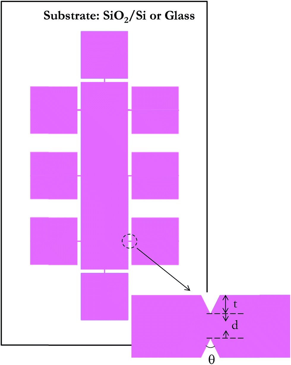 | ||
| Fig. 7 A rectangular electrode in the center is connected by a bridge (see circled region) to smaller square shaped electrodes; the expanded view of the bridge is also shown, in which the bridge is shown to have notches defined by parameters d, t and θ. Once a crack forms at the notch, the rectangular and square electrode pads are separated from each other. | ||
For localizing the cracks in a specified location, it is important to produce a notch that causes sufficient stress concentration at the tip for the crack to propagate here first. Hence, we examine various combinations of parameters d, t and θ, indicated in Fig. 7. Specifically, the design values for these were, wedge-to-wedge separation, d, as 2, 4, 6 and 8 μm and for each of these, the combinations for t and the angle of notches, (t, θ), designed are (2 μm, 90°), (2.5 μm, 70°), (3.5 μm, 50°) and (4 μm, 40°). However, their values actually realized by wet etching (which is available to us, rather than dry etching) at this small scale are significantly different and are noted subsequently.
The preformed substrates of kind shown in Fig. 7, were heated up to a temperature ranging from 300 to 500 °C, to determine the optimum temperature for the formation of cracks for various notch geometries. Further, the heating was performed in vacuum so as to avoid oxidation of metals, especially titanium and also other metals most of which can be used in this process. The temperature was raised at a rate 5 °C per minute and at the set point held for 1 hour.
For illustration, we show one of the bridge in Fig. 8a that has design value of 8 μm wedge-to-wedge separation, t = 4 μm and 40° notch angle before annealing. The measured values from the figure are d = 8.2 μm, t = 2.6 and 2.7 μm (top and bottom notch). Since we employed wet etching (both for making the photo-mask as well as for patterning) which is isotropic, the corners, and even the notch tips, are rounded, therefore angles are not measured. Fig. 8b shows another optical image of a bridge after vacuum annealing at 350 °C, where crack of nanometer width is formed at the notch, as desired. This crack exists only in SiOx layer, that is, it does not pass through the underlying Au films because of the weak interfacial bonding between them and also that Au film is ductile, much less susceptible to sharp cracking. But wet etching of Ti/Au layer through the crack, with SiOx serving as hard mask during etching, and later stripping SiOx leads to the FE-SEM image in Fig. 8c. The nanogap formed in this electrode is ∼200 nm. The nanogap widths were measured for notched electrode bridges with d = 8 μm and θ = 40 °C from a substrate, and the resulting gap is 237 ± 40 nm. Here again, isotropic nature of wet etching results in an undercut/over etching in the Au/Ti films below the SiOx layer, leading to wider gap than created by nanogap crack in SiOx. With the implementation of dry etching and semiconductor processing having stringent process control, such as that available in the industry, the proposed technique may result in controlled formation of nanogaps in electrodes over a large area. The proof of the concept, however, is clearly evident.
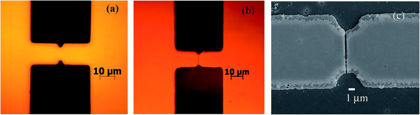 | ||
| Fig. 8 Glass/Ti/Au/SiOx bridge for 40° notch angle and wedge-to-wedge separation of 8 μm, (a) optical image before thermal treatment, (b) optical image after thermal treatment at 350 °C, (c) FE-SEM image of nanogap after etching of Au/Ti layers and SiOx stripping; the gap width is approximately 200 nm. | ||
To check whether nanogaps were electrically isolated or not, they were characterized by electrically probing in air atmosphere at room temperature using Keithley source meter unit. Fig. 9 shows typical isolation behavior of nanogaps formed by this technique.
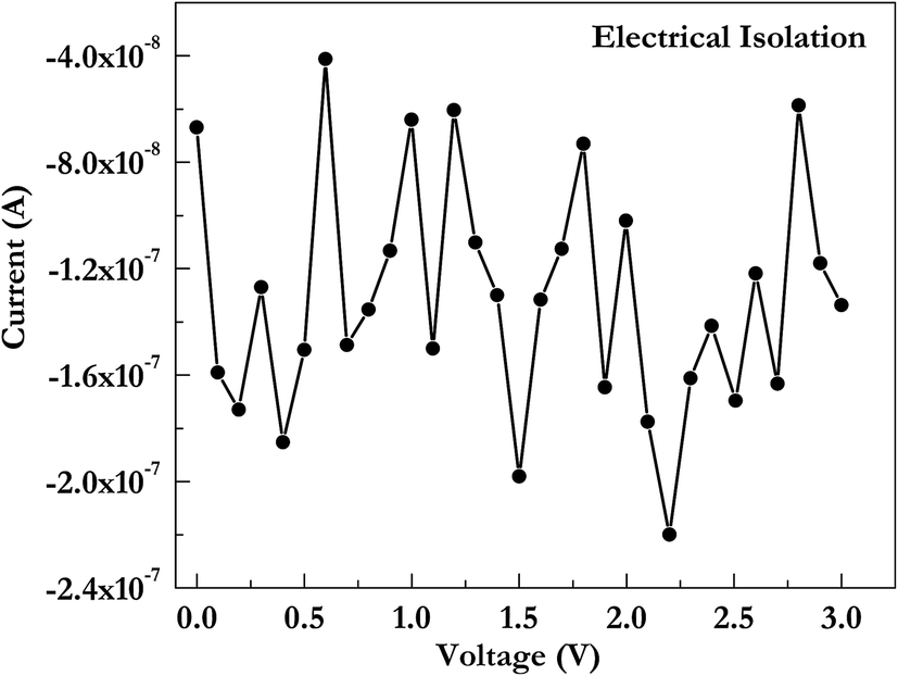 | ||
| Fig. 9 Electrical isolation behavior of the nanogap in Au electrodes having 8 μm wedge-to-wedge separation and 40° notch angle. | ||
This thermal stress induced technique for making nanometer separated electrodes is independent of the substrate. Next, the glass substrate is replaced by, the silicon substrate with thermally grown SiO2. During thermal annealing at 350 °C, there is no crack formation on the thermally grown SiO2 film on Si-substrate. Cracks are formed only at the notched points of the patterned e-beam deposited SiOx on Au/Ti. Fig. 10 shows FE-SEM image of nanogap formed in Au/Ti electrodes on SiO2/Si substrate; here the nanogap is measured after SiOx stripping. The reason for increase in the nanogap dimension may be due to change in the intrinsic stresses in the film being different when deposited on different substrates. Nam et al.28 have also shown that they can control the crack width by controlling the intrinsic stresses during film deposition.
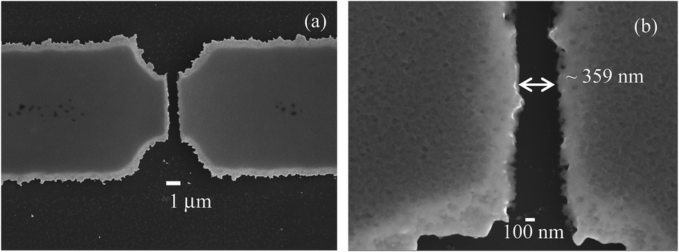 | ||
| Fig. 10 (a) Nanogap formation at the notch in the patterned electrodes of Au/Ti on SiO2/Si-substrate, (b) enlarged one of the nanogap electrode that shows 359 nm gap. | ||
We observed cracks in all cases except where notch formation was not proper due to over etching. In some cases, crack propagation started at both notches on either sides of the bridge width, but did not meet together to form a continuous gap. These were not counted in yield of the process. Mechanism for formation of the gap involves crack initiation at the notch and then its propagation across the bridge due to the brittle nature of SiOx. In spite of the processing issues, the yield observed for 6 μm wedge-to-wedge separation and 40° notch angle is 93% as shown in Fig. 11a. This gives us confidence that with improved processing higher yields will be possible with this technique.
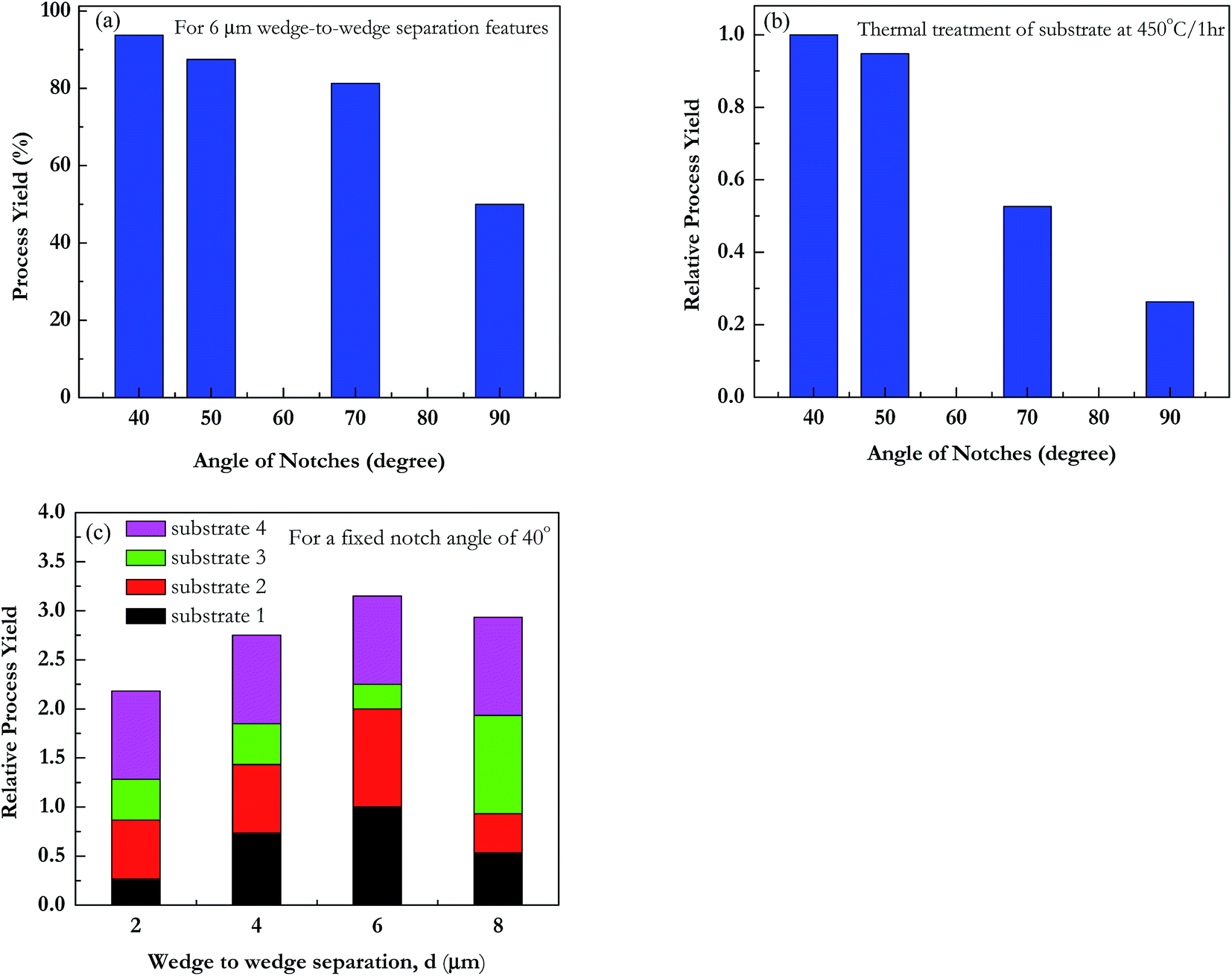 | ||
| Fig. 11 (a) Process yield (%) for notch geometry having d = 6 μm with varying notch angles. (b) Relative process yield as a function of notch angle (θ). Cumulative data from all samples annealed at 450 °C temperature is used. (c) Relative process yield as a function of wedge-to-wedge distance (d) for a fixed notch angle of 40° and annealing temperature 450 °C. | ||
The measured yield of the technique, for forming continuous crack across the bridge at 450 °C annealing temperature, is shown in Fig. 11b for all runs as a function of notch angle. We observe that the maximum yield for crack propagation occurs at notches having design angle 40°. We can conclude that sharp notch geometry is critical for our technique. In Fig. 11c, we also observed that for a given notch angle 40°, wedge-to-wedge separation 6 μm has best yield. However, we can not draw any conclusion at this stage without improving the dimensional accuracy of the notch during optical lithography. We also did not observe significant difference in the yield with the change in annealing temperature.
We have successfully demonstrated that it is possible to simultaneously generate nanogap electrodes across a large substrate. The wet chemical etching during patterning did not allow creation of sharp notch geometries. Further, isotropic nature of Au/Ti wet etching formed an under cut in the Au/Ti films below the SiOx layer, this resulted in rough edges. Using industrial photolithography and dry etching techniques, significantly improved results are expected as notch dimensions can be controlled to higher precision. The proposed idea has advantage of low cost (only micrometer lithography tools), large area and high throughout. Our technique represents an important step towards processing complex integrated nanoelectronics circuits in a single step.
3. Conclusions
Using conventional optical lithography and vacuum heating, nanometer separation between planar electrodes are made across a large area substrate/wafer in a single step. Importance of this lies in the fact that while most techniques for causing separation in nano-dimension are serial process of a wafer, taking substantial time to process even a single wafer, the technique presented here would be carried out on whole wafer (and perhaps a stack of wafers) in one go. In that context, this is a cost effective technique for nanogap fabrication.We have achieved nanogap dimensions ∼150–300 nm using only conventional lithography and subsequent thermal annealing. It may be argued that techniques such as extreme UV and immersion lithography, which are step and repeat could also give similar dimensions. However, we have only provided a proof of concept. It is expected that improved dimensional control using plain and common optical photolithography facility with higher resolution and dry etching of SiOx/Au/Ti stack would give much smaller gaps, depending on the sharpness of the crack. Nanogap size can be further reduced by controlling the intrinsic stress of SiOx film. Here the concept was tested using only Au/Ti electrodes on glass or silicon. However, it is independent of the metal and substrate used, which is also a great advantage.
4. Experimental
4.1 Patterned substrate
Normal borosilicate glass was used as a substrate, prepared by cleaning with soap solutions, followed by cleaning with solutions, RCA1 and RCA2, for removing organic and metal contaminations, respectively. In case of Si-substrate, an highly As doped silicon n++ Si (100) (resistivity < 0.001 Ω cm) covered with 200 nm thin thermally grown SiO2 was used for device fabrication in which doped Si acts as the substrate as well as gate electrode, if needed for transistor measurements. Then, multilayer of Ti (10 nm), Au (50 nm) and SiOx (300 nm) were deposited on the substrate by using e-beam vapor deposition without breaking vacuum in between the deposition steps. For Au film, 10 nm of Ti film was needed as the adhesion promoter to the glass substrate.Using conventional optical lithography process, the patterning of SiOx/Au/Ti layers was first done to form an electrode structure in which a notch is present, as in Fig. 2. This is done by spin-coating a resist layer (TFP 310) on top of multilayer thin films and then exposing the resist by using a photo-mask. After development of exposed area (we used positive photoresist), the latent image of notched electrode bridge was formed on the resist layer. Then the resist pattern was transferred to the SiOx/Au/Ti layers using isotropic chemical etching.
The sequence for chemical etching was from top SiOx film, to Au and finally Ti, while photoresist acted as a mask over the desired notched electrode bridge. Buffer oxide etchant (BOE) was used for SiOx etching. Typically 10 parts 40% NH4F solution to 1 part 49% HF solution by volume was used to prepare BOE solution. The substrate was dipped in BOE etchant for around 2 minutes to etch out 300 nm thick SiOx. Au and Ti layers were patterned using etchant solutions of (KI/I2) and HF, respectively. The mixing ratio of KI![[thin space (1/6-em)]](https://www.rsc.org/images/entities/char_2009.gif) :I2:H2O = 4 g:1 g:250 ml was prepared and used as a warm solution during Au etching. The etching times for Au and Ti layers were around 2 minutes 10 s at 35 °C and 40 s at room temperature, respectively. Finally, the protecting photoresist was stripped off from the patterned notched electrode bridge.
:I2:H2O = 4 g:1 g:250 ml was prepared and used as a warm solution during Au etching. The etching times for Au and Ti layers were around 2 minutes 10 s at 35 °C and 40 s at room temperature, respectively. Finally, the protecting photoresist was stripped off from the patterned notched electrode bridge.
Conflicts of interest
The authors report no competing financial interests.References
- J. A. Liddle and G. M. Gallatin, ACS Nano, 2016, 10, 2995–3014 CrossRef CAS PubMed.
- M. Imboden and D. Bishop, Phys. Today, 2014, 67, 45–50 CrossRef.
- M. A. Reed, C. Zhou, C. J. Muller, T. P. Burgin and J. M. Tour, Science, 1997, 278, 252–254 CrossRef CAS.
- S. Jemmy, L. S. Rosemary and D. C. Scotts, J. Micromech. Microeng., 2010, 20, 045016 CrossRef.
- A. F. Morpurgo, C. M. Marcus and D. B. Robinson, Appl. Phys. Lett., 1999, 74, 2084–2086 CrossRef CAS.
- G. J. Dolan, Appl. Phys. Lett., 1977, 31, 337–339 CrossRef.
- D. Gupta, S. S. K. Iyer, M. Katiyar and D. Gupta, Indian Patent, Application No. 1775/DEL/2004, 2004.
- D. E. Johnston, D. R. Strachan and A. T. C. Johnson, Nano Lett., 2007, 7, 2774–2777 CrossRef CAS PubMed.
- T. M. B. Mordechai Rothschild, T. H. Fedynyshyn, R. R. Kunz, V. Liberman, M. Switkes, N. N. Efremow Jr, S. T. Palmacci, J. H. C. Sedlacek, D. E. Hardy and A. Grenville, Linc. Lab. J., 2003, 14, 221–236 Search PubMed.
- C. Wagner and N. Harned, Nat. Photon., 2010, 4, 24–26 CrossRef CAS.
- T. Nagase, T. Kubota and S. Mashiko, Thin Solid Films, 2003, 438, 374–377 CrossRef.
- L. D. Menard and J. M. Ramsey, Nano Lett., 2011, 11, 512–517 CrossRef CAS PubMed.
- J. A. Dagata, J. Schneir, H. H. Harary, C. J. Evans, M. T. Postek and J. Bennett, Appl. Phys. Lett., 1990, 56, 2001–2003 CrossRef CAS.
- E. S. Snow and P. M. Campbell, Science, 1995, 270, 1639–1641 CAS.
- M. S. M. Saifullah, T. Ondarçuhu, D. K. Koltsov, C. Joachim and M. E. Welland, Nanotechnology, 2002, 13, 659 CrossRef CAS.
- J. B. Lee, P. C. Chang, J. A. Liddle and V. Subramanian, IEEE Trans. Electron Devices, 2005, 52, 1874–1879 CrossRef CAS.
- R. D. Piner, J. Zhu, F. Xu, S. Hong and C. A. Mirkin, Science, 1999, 283, 661–663 CrossRef CAS PubMed.
- K. Salaita, S. W. Lee, X. Wang, L. Huang, T. M. Dellinger, C. Liu and C. A. Mirkin, Small, 2005, 1, 940–945 CrossRef CAS PubMed.
- H. Schift, J. Vac. Sci. Technol., B: Microelectron. Nanometer Struct.--Process., Meas., Phenom., 2008, 26, 458–480 CrossRef CAS.
- J. R. Maldonado and M. Peckerar, Microelectron. Eng., 2016, 161, 87–93 CrossRef CAS.
- G. Purohit, D. Gupta and M. Katiyar, Indian Patent, Provisional patent application number - 194/DEL/2015, 2015.
- T. Nishibe, J. Vac. Sci. Technol., B: Microelectron. Nanometer Struct.--Process., Meas., Phenom., 1995, 13, 1429–1433 CrossRef CAS.
- H.-I. Lee, S.-S. Park, D.-I. Park, S.-H. Hahm, J.-H. Lee and J.-H. Lee, J. Vac. Sci. Technol., B: Microelectron. Nanometer Struct.--Process., Meas., Phenom., 1998, 16, 762–764 CrossRef CAS.
- P. Dong-Il, Z. Woo-Jae, L. Jong-Hyun, L. Jung-Hee and H. Sung-Ho, Jpn. J. Appl. Phys., 1998, 37, 7205 CrossRef.
- F.-M. Iván, G. Yolanda and B. Fernando, Nanotechnology, 2008, 19, 275302 CrossRef PubMed.
- B. E. Alaca, H. Sehitoglu and T. Saif, Appl. Phys. Lett., 2004, 84, 4669–4671 CrossRef CAS.
- R. Adelung, O. C. Aktas, J. Franc, A. Biswas, R. Kunz, M. Elbahri, J. Kanzow, U. Schurmann and F. Faupel, Nat. Mater., 2004, 3, 375–379 CrossRef CAS PubMed.
- K. H. Nam, I. H. Park and S. H. Ko, Nature, 2012, 485, 221–224 CrossRef CAS PubMed.
- M. Kim, D. Ha and T. Kim, Nat. Commun., 2015, 6, 6247 CrossRef CAS PubMed.
- Q. Zhao, W. Wang, J. Shao, X. Li, H. Tian, L. Liu, X. Mei, Y. Ding and B. Lu, Adv. Mater., 2016, 28, 6337–6344 CrossRef CAS PubMed.
- V. Dubois, F. Niklaus and G. Stemme, Adv. Mater., 2016, 28, 2178–2182 CrossRef CAS PubMed.
- A. Cui, Z. Liu, H. Dong, Y. Wang, Y. Zhen, W. Li, J. Li, C. Gu and W. Hu, Adv. Mater., 2015, 27, 3002–3006 CrossRef CAS PubMed.
- A. Cui, Z. Liu, H. Dong, Y. Wang, Y. Zhen, W. Li, J. Li, C. Gu and W. Hu, Sci. China Mater., 2015, 58, 769–774 CrossRef CAS.
- V. Dubois, F. Niklaus and G. Stemme, Microsyst. Nanoeng., 2017, 3, 17042 CrossRef.
- http://www.pgo-online.com/intl/katalog/borofloat.html.
- N. Bouras, M. A. Madjoubi, M. Kolli, S. Benterki and M. Hamidouche, Phys. Procedia, 2009, 2, 1135–1140 CrossRef CAS.
- M. C. Salvadori, I. G. Brown, A. R. Vaz, L. L. Melo and M. Cattani, Phys. Rev. B, 2003, 67, 153404 CrossRef.
- M. C. Salvadori, A. R. Vaz, L. L. Melo and M. Cattani, Surf. Rev. Lett., 2003, 10, 571–575 CrossRef CAS.
- M. C. S. A. R. Vaz and M. Cattani, J. Metastable Nanocryst. Mater., 2004, 20–21, 758–762 CrossRef.
- J. W. N. Sharpe, J. Pulskamp, B. G. Mendis, C. Eberl, D. S. Gianola, R. Polcawich and K. J. Hemker, ASME International Mechanical Engineering Congress and Exposition, 2006, vol. 13290, pp. 533–540 Search PubMed.
- J. Lai, T. Perazzo, Z. Shi and A. Majumdar, Sens. Actuators, A, 1997, 58, 113–119 CrossRef CAS.
- C.-W. Baek, Y.-K. Kim, Y. Ahn and Y.-H. Kim, Sens. Actuators, A, 2005, 117, 17–27 CrossRef CAS.
- T. C. Hodge, S. A. Bidstrup-Allen and P. A. Kohl, IEEE Trans. Compon. Packag. Manuf. Technol., 1997, 20, 241–250 CrossRef CAS.
- J. D. Plummer, M. D. Deal and P. B. Griffin, Silicon VLSI Technology-Fundamentals, Practice and Modeling, Pearson Education Inc., Prentice Hall, p. 697 Search PubMed.
- H. D. Espinosa and B. C. Prorok, J. Mater. Sci., 2003, 38, 4125–4128 CrossRef CAS.
- H. D. Espinosa, B. C. Prorok and M. Fischer, J. Mech. Phys. Solid., 2003, 51, 47–67 CrossRef CAS.
- S. Okuda, M. Kobiyama and T. Inami, Mater. Trans. JIM, 1999, 40, 412–415 CrossRef CAS.
- https://ocw.mit.edu/courses/materials-science-and-engineering/3-11-mechanics-of-materials-fall-1999.
- M. W. Barsoum, Fundamentals of Ceramics, IOP Publishing Ltd., 2003, p. 363 Search PubMed.
- H. Hosokawa, A. V. Desai and M. A. Haque, Thin Solid Films, 2008, 516, 6444–6447 CrossRef CAS.
- S. Olliges, P. A. Gruber, S. Orso, V. Auzelyte, Y. Ekinci, H. H. Solak and R. Spolenak, Scr. Mater., 2008, 58, 175–178 CrossRef CAS.
- V. Hatty, H. Kahn and A. H. Heuer, J. Microelectromech. Syst., 2008, 17, 943–947 CrossRef CAS.
- J. Malzbender and G. de With, J. Non-Cryst. Solids, 2000, 265, 51–60 CrossRef CAS.
Footnote |
| † Electronic supplementary information (ESI) available. See DOI: 10.1039/c8ra00278a |
| This journal is © The Royal Society of Chemistry 2018 |